Note: Descriptions are shown in the official language in which they were submitted.
CA 02611150 2007-12-05
WO 2006/131215 1 PCT/EP2006/004975
ELECTRICAL CONNECTOR
The invention relates generally to electrical connectors and, more
particularly, to an
electrical connector for transmitting signals in differential pairs.
With the ongoing trend toward smaller, faster, and higher performance
electrical
components such as processors used in computers, routers, switches, etc., it
has
become increasingly important for the electrical interfaces along the
electrical paths to
also operate at higher frequencies and at higher densities with increased
throughput.
In a traditional approach for interconnecting circuit boards, one circuit
board serves as a
back plane and the other as a daughter board. The back-plane typically has a
connector,
commonly referred to as a header, that includes a plurality of signal pins or
contacts
which connect to conductive traces on the back plane. The daughter board
connector,
commonly referred to as a receptacle, also includes a plurality of contacts or
pins.
Typically, the receptacle is a right angle connector that interconnects the
back plane with
the daughter board so that signals can be routed between the two. The right
angle
connector typically includes a mating face that receives the plurality of
signal pins from
the header on the back plane, and contacts that connect to the daughter board.
At least some board-to-board connectors are differential connectors wherein
each signal
requires two lines that are referred to as a differential pair. For better
performance, a
ground contact is associated with each differential pair. The receptacle
connector
typically includes a number of modules having contact edges that are at right
angles to
each other. The modules may or may not include a ground shield. As the
transmission
frequencies of signals through these connectors increase, it becomes more
desirable to
maintain a desired impedance through the connector to minimize signal
degradation. A
ground shield is sometimes provided on the module to reduce interference or
crosstalk.
In addition, a ground shield may be added to the ground contacts on the header
connector. Improving connector performance and increasing contact density to
increase
signal carrying capacity without increasing the size of the connectors is
challenging.
Some older connectors, which are still in use today, operate at speeds of one
gigabit per
second or less. By contrast, many of today's high performance connectors are
capable
of operating at speeds of up to ten gigabits or more per second. As would be
expected,
the higher performance connector also comes with a higher cost.
CA 02611150 2007-12-05
WO 2006/131215 2 PCT/EP2006/004975
US 6,808,420, granted to the applicant of the present application on October
26, 2004,
discloses an electrical connector comprising a connector housing holding
signal contacts
and ground contacts in an array organized into rows. Each row includes pairs
of the
signal contacts and some of the ground contacts arranged in a pattern, wherein
adjacent
first and second rows have respective different first and second patterns.
US 6,379,188, granted on April 30, 2002, shows an electrical connector for
transferring a
plurality of differential signals between electrical components. The connector
is made of
modules that have a plurality of pairs of signal conductors with a first
signal path and a
second signal path.
Electrical connectors according to the prior art comprise a plurality of
contacts embedded
in a plastic housing. Figure 1 shows a plurality of mating contacts 3 in such
an electrical
connector represented without the plastic housing. Each mating contact 3 is
electrically
connected to a corresponding mounting contact 6 by a conductor 5. The
plurality of
conductors 5 connecting mounting contacts 6 with the corresponding mating
contacts 3
arranged on one of the rows, constitutes a so-called lead frame, an example of
which is
represented in figure 2.
Figure 3 shows a cross-sectional view of the plurality of conductors 5 shown
in figure 1,
taken along one of the lines A-A, B-B or C-C. In such an electrical connector
according to
the prior art, the plurality of conductors 5 have electrical characteristics,
which may vary
depending on the position of a particular conductor within the electrical
connector.
Indeed, the conductors located in the outer regions of said electrical
connector, identified
in figure 3 by the conductors represented in black, have electrical
characteristics that
vary from the electrical characteristics of the conductor arranged in the
inner regions of
the electrical connector, represented by the white conductors in figure 3. In
particular, the
total capacitance of the individual conductors arranged in the outer regions
of such an
electrical connector is typically lower than the total capacitance of the
conductors located
in the inner regions of the electrical connector. This phenomenon is due to
the fact that
the conductors in the outer regions do not have neighbors on one side, which
results in
non-uniform electrical characteristics. These non-uniform electrical
characteristics may
lead to a degradation of the signals transmitted by the electrical connector.
CA 02611150 2012-09-18
31255-4
3
An object of some embodiments is therefore to provide an electrical connector
with
improved electrical characteristics, such as reduced crosstalk and uniform
electrical
properties of its conductors.
This object is solved by an electrical connector and by a lead frame according
to
some embodiments disclosed herein.
According to a first aspect of the present invention, an electrical connector
is provided
that comprises a housing and a plurality of contact modules in said housing,
each said
contact module comprising a mating edge and a mounting edge, each said mating
and
mounting edge having a row of contacts including signal contacts and ground
contacts.
Each mating edge contact is electrically connected to a corresponding mounting
edge
contact by signal conductors and ground conductors extending along a
predetermined
path within said contact module to form a lead frame in each contact module,
said
ground conductors and signal conductors being arranged in an adjacent
relationship to
provide electrical shielding. The signal conductors and ground conductors of
several
contact modules are arranged, when seen in a cross-sectional view through the
lead
frames, in an array having outer and inner layers, wherein at least a portion
of the signal
conductors and ground conductors in the outer layers has a width transverse to
said
predetermined path that is different from a width transverse to said
predetermined path
of the signal conductors and ground conductors in the inner layers.
By changing the shape of the signal conductors and ground conductors in the
outer
layers, in particular, by changing the width of the signal conductors and
ground
conductors in the outer layers, the electrical characteristics of the
conductors in an
electrical connector can be made uniform. Indeed, changing the width of at
least a
portion of the outer signal conductors and ground conductors in the outer
layers allows to
reduce the difference in total capacitance between the plurality of contacts
comprised in
one lead frame. The fact that the outer conductors, located at one end of the
lead frame,
do not have neighbors on one side, can therefore be compensated.
According to a second aspect of the present invention, an electrical connector
is
provided, which comprises a housing and a plurality of contact modules in said
housing,
each said contact module comprising a mating edge and a mounting edge, each
said
CA 02611150 2007-12-05
WO 2006/131215 4 PCT/EP2006/004975
mating and mounting edge having a row of contacts including signal contacts
and ground
contacts. Each mating edge contact is electrically connected to a
corresponding
mounting edge contact by signal conductors and ground conductors extending
along a
predetermined path within said contact module to form a lead frame in each
contact
module, said ground conductors and signal conductors being arranged in an
adjacent
relationship to provide electrical shielding. The signal conductors and ground
conductors
of several contact modules are arranged, when seen in a cross-sectional view
through
the lead frames, in an array having outer and inner layers, wherein a pitch
between the
outer layers is different from a pitch between the inner layers.
By changing the spatial arrangement of the outer conductors, in particular, by
foreseeing
a pitch between the outer conductors that is different from a pitch between
the inner
conductors, the electrical properties of the conductors within said electrical
connector
can be made uniform.
According to a preferred embodiment of the present invention, an electrical
connector is
provided, wherein the width of the signal conductors and ground conductors in
the outer
layers, is different from the width of the signal conductors and ground
conductors in the
inner layers and a pitch between the outer layers is different from a pitch
between the
inner layers. Foreseeing such an electrical connector allows to achieve
uniform electrical
characteristics of the conductors within said electrical connector.
According to a further embodiment of the present invention, the signal
conductors and
ground conductors are arranged in one of a first and second pattern, adjacent
contact
modules in said housing having a different one of said first and second
patterns, each
said first and second patterns including pairs of signal conductors and
individual ground
conductors arranged in an alternating sequence. Each said ground conductor has
a
width transverse to said predetermined path that is substantially equal to a
combined
transverse width across a pair of signal conductors in an adjacent contact
module, said
ground conductor thereby shielding said pair of signal conductors in said
adjacent
contact module.
Since the lead frames in adjacent contact modules have different conductor
patterns, the
signal conductors arranged in differential pairs can be shielded by adjacent
ground
conductors to reduce crosstalk in the electrical connector and facilitate
increased
throughput through the electrical connector. Further shielding for the signal
conductors
CA 02611150 2007-12-05
WO 2006/131215 5 PCT/EP2006/004975
can be provided by the ground conductors above and below the signal conductors
within
the same lead frame, which cooperate with the ground conductors in an adjacent
lead
frame to substantially isolate each differential signal pair from other
differential signal
pairs in the electrical connector.
Alternatively, the signal conductors and ground conductors of the electrical
connector
can be arranged in one of a first and second pattern, adjacent contact modules
in said
housing having a different one of said first and second patterns, said first
and second
patterns each including pairs of signal conductors and pairs of ground
conductors
arranged in an alternating sequence. Each said pair of ground conductors has a
combined transverse width to said predetermined path that is substantially
equal to a
combined transverse width across a pair of signal conductors in an adjacent
contact
module, said pair of ground conductors thereby shielding said pair of signal
conductors in
said adjacent contact module.
In the electrical connector according to this particular embodiment, a pair of
ground
conductors ensures electrical shielding of a pair of signal conductors in the
adjacent
contact module. In this manner, the signal conductors arranged in different
pairs can be
shielded by a pair of adjacent ground conductors to reduce crosstalk in the
electrical
connector. Further, since a pair of shielding ground conductors is arranged in
correspondence with a pair of signal conductors in the adjacent lead frame,
different
assignments of the signal conductors and ground conductors can be achieved,
which is
particularly advantageous when high data rates are not required.
According to another aspect of the present invention, a lead frame for an
electrical
contact module is provided, which comprises a first row of contacts comprising
mating
contacts and defining a mating edge, and a second row of contacts comprising
mounting
contacts and defining a mounting edge. Each first row of mating contacts and
each
second row of mounting contacts includes signal contacts and ground contacts,
each
mating edge signal and ground contact being electrically connected to a
corresponding
mounting edge signal and ground contact by first and second conductors
extending
along the predetermined path within the lead frame. At least a portion of the
first
conductors connecting the mating contacts and mounting contacts arranged at an
end of
said first and second row has a width transverse to said predetermined path
that is
different from the width transverse to said predetermined path of the second
conductors
connecting the mating contacts and the mounting contacts of said first and
second rows.
CA 02611150 2007-12-05
WO 2006/131215 6 PCT/EP2006/004975
According to an advantageous embodiment of the lead frame according to the
present
invention, the first conductors are essentially outer conductors of the lead
frame and the
second conductors are essentially inner conductors of the lead frame.
Foreseeing at
least a portion of the outer conductors of the lead frame with a width that is
different from
a width of the inner conductors of the lead frame allows to improve the
electrical
characteristics of the lead frame, in particular, it is possible to obtain a
lead frame in
which the conductors have more uniform electrical properties. Hence, there is
a smaller
difference between the electrical properties of the outer conductors and those
of the
inner conductors, thus guaranteeing a high signal integrity. This aspect is
particularly
advantageous when several lead frames are integrated into one electrical
connector
transmitting information signals, as such an electrical connector implementing
a plurality
of lead frames according to the present invention may transport information
signals while
guaranteeing very low signal degradation.
According to yet another embodiment of the lead frame according to the present
invention, a lead frame is provided that comprises a first row of contacts
comprising
mating contacts and defining a mating edge and a second row of contacts
comprising
mounting contacts and defining a mounting edge. Each row of mating contacts
and
mounting contacts includes signal contacts and ground contacts, each mating
edge
signal and ground contact being electrically connected to a corresponding
mounting
edge signal and ground contact by first and second conductors extending along
the
predetermined path within the lead frame. A pitch between two adjacent first
conductors
connecting the mating contacts and mounting contacts arranged at an end of
said first
and second row is different from a pitch between two adjacent second
conductors
connecting the mating contacts and mounting contacts of said first and second
row.
It is particularly advantageous to foresee said first conductors as outer
conductors of said
lead frame and said second conductors as inner conductors of said lead frame,
wherein
the pitch between two adjacent outer conductors is different from the pitch
between two
adjacent inner conductors. Such a lead frame has the advantage of comprising
conductors with uniform electrical characteristics. When implementing such a
lead frame
in an electrical connector that transports information signals, an electrical
connector can
be provided that has the advantage of transporting information signals while
guaranteeing a high signal integrity.
CA 02611150 2012-09-18
31255-4
7
According to a preferred embodiment of the present invention, a contact
assembly is
provided, which comprises at least a first and second lead frame according to
the
present invention, said second lead frame being adjacent to the first lead
frame. The
signal conductors and ground conductors of the first lead frame are arranged
in one of a
first and second pattern, each said first and second patterns including pairs
of signal
conductors and individual ground conductors arranged in an alternating
sequence. Each
ground conductor of said first lead frame has a width transverse to said
predetermined
path that is substantially equal to a combined transverse width across a pair
of signal
conductors in the second adjacent lead frame having conductors arranged in the
other of
said patterns, the ground conductor of the first lead frame thereby shielding
the pair of
signal conductors in the second adjacent lead frame.
Alternatively, a contact assembly is provided, which comprises at least a
first and a
second lead frame according to the present invention, the second lead frame
being
adjacent to the first lead frame. The signal conductors and ground conductors
of the first
lead frame are arranged in one of a first and second pattern. Each first and
second
patterns include pairs of signal conductors and pairs of ground conductors
arranged in
an alternating sequence. Each pair of ground conductors of the first lead
frame has a
combined transverse width to the predetermined path that is substantially
equal to a
combined transverse width across a pair of signal conductors in the second
adjacent
lead frame having conductors arranged in the other of said patterns, the pair
of ground
conductors of the first lead frame thereby shielding the pair of signal
conductors in the
second adjacent lead frame.
CA 02611150 2012-09-18
31255-4
7a
According to one aspect of the present invention, there is provided an
electrical
connector comprising: a housing, and a plurality of contact modules in said
housing,
wherein each contact module comprising a mating edge and a mounting edge, each
mating and mounting edge having a row of contacts including signal contacts
and
ground contacts, each mating edge contact being electrically connected to a
corresponding mounting edge contact by signal conductors and ground conductors
extending along a predetermined path within said contact module to form a lead
frame in each contact module, said ground conductors and signal conductors
being
arranged in an adjacent relationship to provide electrical shielding, and said
signal
conductors and ground conductors of several contact modules being arranged,
when
seen in a cross-sectional view through the lead frames, in an array having
outer and
inner layers, wherein: said signal conductors and ground conductors are
arranged in
one of a first and second pattern, adjacent contact modules in said housing
have a
different one of said first and second patterns, said first and second
patterns each
including pairs of signal conductors and individual ground conductors arranged
in an
alternating sequence, and each said ground conductor has a width transverse to
said
predetermined path that is substantially equal to a combined transverse width
across
a pair of signal conductors in an adjacent contact module, said ground
conductor
thereby shielding said pair of signal conductors in said adjacent contact
module.
According to another aspect of the present invention, there is provided an
electrical
connector, comprising: a dielectric housing provided with a plurality of
contact
modules, each of the contact modules provided with a lead frame having
mounting
contacts electrically connected to mating contacts by signal conductors and
ground
conductors that extend along a predetermined path within the contact module;
the
lead frames in adjacent contact modules alternating between a first pattern
and a
second pattern, the first pattern and the second pattern each having pairs of
signal
conductors and individual ground conductors arranged in an alternating
sequence;
and each of the ground conductors having a width transverse to the
predetermined
CA 02611150 2012-09-18
31255-4
7b
path that is substantially equal to a combined width transverse to the
predetermined
path across the pair of signal conductors in the adjacent contact module such
that the
ground conductor shields the pair of signal conductors in the adjacent contact
module.
According to still another aspect of the present invention, there is provided
an
electrical connector, comprising: a dielectric housing provided with a
plurality of
contact modules, each of the contact modules provided with a lead frame having
mounting contacts electrically connected to mating contacts by signal
conductors and
ground conductors that extend along a predetermined path within the contact
module;
the lead frames in adjacent contact modules alternating between a first
pattern and a
second pattern, the first pattern and the second pattern each having pairs of
signal
conductors and pairs of ground conductors arranged in an alternating sequence;
and
each of the pairs of ground conductors having a combined width transverse to
the
predetermined path that is substantially equal to a combined width transverse
to the
predetermined path across the pair of signal conductors in the adjacent
contact
module such that the pair of ground conductors shields the pair of signal
conductors
in the adjacent contact module.
The present invention will be described in detail in the following based on
the figures
enclosed with the application:
Figure 1 is a perspective view of the plurality of lead frames within one
electrical
connector according to the prior art;
Figure 2 is a side view of one lead frame according to the prior art;
Figure 3 is a cross-sectional view of the plurality of lead frames shown in
Figure 1
taken along one of the lines A-A, B-B or C-C shown in Figure 2;
Figure 4 is a side view of a female electrical connector according to the
present
invention mated with a male connector;
CA 02611150 2012-09-18
31255-4
7c
Figure 5 is a side view of a multi-board arrangement implementing the
electrical
connectors according to the present invention;
CA 02611150 2007-12-05
WO 2006/131215 8 PCT/EP2006/004975
Figure 6 is a perspective view of a female electrical connector according to
the
present invention;
Figure 7 is a perspective view of a male electrical connector according to the
present invention;
Figure 8 is a perspective view of a multi-board arrangement comprising two
female
electrical connectors according to the present invention;
Figure 9 is a perspective view of the plurality of lead frames according to
one
embodiment of the present invention;
Figure 10 is a side view of a lead frame according to one embodiment of the
present
invention;
Figure 11 is a side view of a lead frame adjacent to the lead frame of Figure
10;
Figure 12 is a cross-sectional view of an electrical connector according to
the present
invention, taken along the line D-D shown in figures 10 and 11;
Figure 13 is a cross-sectional view of the electrical connector according to a
preferred embodiment of the present invention, taken along the line D-D
shown in figures 10 and 11;
Figure 14 is a cross-sectional view of the plurality of lead frames shown in
figure 9,
taken along one of the lines E-E or F-F shown in figures 10 and 11;
Figure 15 is a cross-sectional view of the plurality of lead frames according
to a
preferred embodiment of the present invention, taken along one of the lines
E-E or F-F shown in Figures 10 and 11;
Figure 16 is a cross-sectional view of the plurality of lead frames according
to a
further embodiment of the present invention, taken along one of the lines
E-E or F-F.
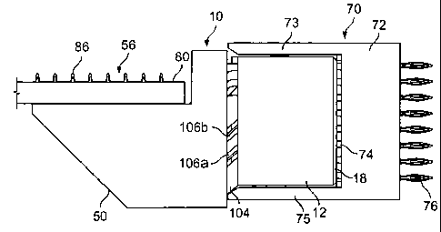
Figure 4 illustrates an electrical connector 10 formed in accordance with an
exemplary
embodiment of the present invention. While the electrical connector 10 will be
described
with particular reference to a receptacle connector, a right-angle connector
interconnecting a back-plane with a daughter board, it is to be understood
that the
benefits described herein are also applicable to other connectors in
alternative
embodiments.
The electrical connector 10 includes a dielectric housing 12. A plurality of
contact
modules 50 are connected to the housing 12. The contact modules 50 define a
mounting
face 56, which comprises a plurality of mounting contacts 86. In a preferred
embodiment,
the mounting face 56 is substantially perpendicular to the mating face 18 of
the dielectric
CA 02611150 2007-12-05
WO 2006/131215 9 PCT/EP2006/004975
housing 12, such that the electrical connector 10 interconnects electrical
components
that are substantially at a right angle to one another. The mounting contacts
86 are
adapted to be mounted on a circuit board 80. The dielectric housing 12
includes a
plurality of mating contacts that are accessible to corresponding mating
elements
through a mating face 18 of the dielectric housing 12. A plurality of ground
conductors
104 and signal conductors 106a, 106b connect the mounting contacts 86 and
mating
contacts.
A connector 70 comprising mating elements can be mated with the mating
contacts of
the electrical connector 10. The connector 70 comprises a plastic body 72 in
which
mating elements 76 are embedded. The plastic body 72 of the connector 70
comprises
two side parts 73, 75. The mating elements 76 are embedded in the plastic body
72 in
such a way that a longitudinal axis of the mating elements 76 is parallel to a
longitudinal
axis of the side parts 73, 75. The plastic body 72 comprises a hollow part
arranged
between side parts 73, 75, said hollow part having dimensions such that the
housing 12
of the electrical connector 10 can be fitted into said hollow part of the
connector 70.
The mating elements 76 of said connector 70 protrude out of the plastic body
72 on the
side of the connector 70 oriented towards the hollow part in which the housing
12 of the
electrical connector 10 can be fitted. The mating elements 76 protrude towards
the
hollow part of the connector 70 in mating element ends 74. The mating element
ends 74
can be introduced through the mating face 18 of the dielectric housing 12 to
mate with
the mating contacts of the electrical connector 10.
Figure 5 shows a multi-board arrangement comprising a board 80 on which an
electrical
connector 10 is mounted, a board 80' on which an electrical connector 10' is
mounted
and a board 80" on which an electrical connector 10" is mounted. A connector
70'
connects the boards 80, 80', 80" electrically. The connector 70' is formed
essentially of
two connectors 70 as shown in figure 4.
The first board 80, on which the first electrical connector 10 is mounted and
the second
board 80', on which the second electrical connector 10' is mounted, are
arranged in an
essentially co-planar position. The housing of the first electrical connector
10 is received
in a first hollow part, located between first side parts 73, 75 of the mating
connector 70'.
The housing of the second electrical connector 10' is received in a second
hollow part
located between a side part 73' and a side part 75' adjacent to side part 75
of the
CA 02611150 2007-12-05
WO 2006/131215 10 PCT/EP2006/004975
connector 70'. On the face of the plastic body 72 of the connector 70', which
is oriented
opposite to the first and second hollow parts, the third electrical connector
10" mounted
on the third board 80" is mated with the first electrical connector 10 through
the
connector 70'. The first electrical connector 10 and the third electrical
connector 10" are
mated in such a way through the connector 70' that the first board 80 and the
third board
80" are in a co-planar arrangement.
Figure 6 shows a female electrical connector 10 according to the present
invention. The
mounting contacts 86 of the electrical connector 10 are mounted on the
electric board
80. The housing 12 of the electrical connector 10 comprises a mating face 18
including a
plurality of contact cavities 22 that are configured to receive corresponding
mating
elements. Further, the housing 12 comprises an alignment rib 42 arranged on an
upper
face 32 of said housing 12. The alignment rib 42 allows to bring the
electrical connector
10 into alignment with the connector 70 during the mating process so that the
mating
element ends 74 of the mating connector 70 are received in the contact
cavities 22
without damage.
Figure 7 illustrates a male electrical connector according to the present
invention. A
connector 70' has two hollow parts comprised respectively between a side part
73' and a
central side part 75, and between said central side part 75 and a side part
73. Mating
element ends 74 and 74' are arranged in the respective hollow parts of the
plastic body
72 of the mating connector 70'. The mating element ends 74, 74' arranged in
the
respective hollow parts are male mating elements, which are adapted to be
mated with
the mating contacts in the contact cavities 22 of the mating face 18 of a
first electrical
connector 10 and with the mating contacts in the contact cavities of a mating
face of a
second electrical connector 10'.
Figure 8 shows a multi-board arrangement as shown in figure 5, wherein a first
electrical
connector 10 is mounted on a first board 80 and a second electrical connector
10' is
mounted on a second board 80'. Each electrical connector 10, 10' is adapted to
be
mated with each connector 70, 70'. In particular, the mating contacts of the
respective
mating face 18, 18' of each electrical connector 10, 10' are mated with the
respective
mating element ends 74, 74' of each respective connector 70, 70'.
Figure 9 shows a perspective view of a plurality of lead frames 100, 200 that
are
arranged within one electrical connector 10 according to the present
invention. The lead
CA 02611150 2007-12-05
WO 2006/131215 11 PCT/EP2006/004975
frames 100, 200 comprise a plurality of conductors. The conductors extend
along a
predetermined path to electrically connect each mating edge contact 82 to a
corresponding mounting edge contact 86. The mating edge is essentially
perpendicular
to the mounting edge 56.
Figure 10 is a side view of a lead frame 100 that includes a plurality of
conductors 102
including ground conductors 104 and signal conductors 106a, 106b that extend
along the
predetermined path to electrically connect each mating edge contact 82 to a
corresponding mounting edge contact 86.
The mating contacts 82 and mounting contacts 86 include both signal and ground
contacts that are connected to one another by corresponding signal conductors
106a,
106b and ground conductors 104. The ground conductors 104 and signal
conductors
106a, 106b are arranged in a first pattern that includes pairs of signal
conductors 106a,
106b and individual ground contacts 104 arranged in an alternating sequence.
For
example, in the first pattern shown in figure 10, the ground conductor 104 is
foreseen in
the form of a shielding blade that is arranged in an adjacent position to the
pair of signal
conductors 106a, 106b within the lead frame 100.
Figure 11 shows a side view of the lead frame 200, adjacent to the lead frame
100
shown in figure 10. The lead frame 200 comprises a plurality of conductors 202
including
signal conductors 206a, 206b and ground conductors 204 that extend along the
predetermined path to electrically connect each mating edge contact 82 to a
corresponding mounting edge contact 86.
The ground conductors 204 and signal conductors 206a, 206b in figure 11 are
arranged
in a second pattern that includes pairs of signal conductors 206a, 206b and
individual
ground contacts 204 arranged in an alternating sequence. The ground conductor
204 is
foreseen in the form of a shielding blade that is arranged on one end of the
lead frame
200. A pair of signal conductors 206a, 206b is arranged closest to the
shielding blade
forming the ground conductor 204. This sequence according to the second
pattern is
therefore designed in such a way that the pair of signal conductors 206a, 206b
and the
individual ground conductor 204 are arranged in an alternating sequence to the
sequence shown in figure 10.
CA 02611150 2007-12-05
WO 2006/131215 12 PCT/EP2006/004975
The ground conductors 204 of the lead frame 200 shown in figure 11 have a
width
transverse to the longitudinal path of the ground conductors 204 that is
substantially
equal to a combined transverse width of the pair of signal conductors 106a,
106b of the
adjacent lead frame 100 shown in figure 10. Likewise, the ground conductors
104 of the
lead frame 100 shown in figure 10 have a width transverse to the longitudinal
path of the
ground conductors 104 that is substantially equal to a combined transverse
width of the
pair of signal conductors 206a, 206b of the adjacent lead frame 200 shown in
figure 11.
In this manner, the ground conductors 104, 204 shield the signal conductors
106a, 106b,
206a, 206b in the mutual adjacent lead frame 100, 200.
Figure 12 shows a cross-sectional view of the mating edge of the plurality of
lead frames
100, 200, taken along the line D-D shown in figures 10 and 11.
The plurality of signal conductors 106a, 106b, 206a, 206b and ground
conductors 104,
204 are arranged in an array, when seen in a cross-sectional view through the
lead
frames 100, 200, taken along the line D-D. In a preferred embodiment, the
signal
conductors 106a, 106b, 206a, 206b and ground conductors 104, 204 are arranged
in an
essentially rectangular or square array, as represented in figure 12.
The conductors in figure 12 are shown either in white to identify the signal
conductors or
black to identify the ground conductors. Moreover, a grid characterized by the
numbers 1
to 6 and the letters A to H allows to identify the array of signal conductors
and ground
conductors. The plurality of lead frames 100, 200 are arranged in an
alternating
sequence, such that two adjacent lead frames 100, 200 have different conductor
patterns. Specifically, the lead frames 100, 200 are configured such that the
signal
conductors 106a, 106b, 206a, 206b in each of the lead frames 100, 200 are
spatially
aligned with the ground conductor 104, 204 in an adjacent lead frame 100, 200.
Likewise, the signal conductors 106a, 106b, 206a, 206b in each of the lead
frames 100
200 are spatially aligned with the ground conductor 104, 204 in an adjacent
lead frame
100.
In this manner, the signal conductors 106a, 106b, 206a, 206b arranged in
differential
pairs are shielded by adjacent ground conductors 104, 204 to reduce crosstalk
in the
electrical connector 10 and facilitate increased throughput through the
electrical
connector 10. Further shielding for the signal conductors 106a, 106b, 206a,
206b is
provided by ground conductors 104, 204 above and below the signal conductors
106a,
CA 02611150 2007-12-05
WO 2006/131215 13 PCT/EP2006/004975
106b, 206a, 206b in the same lead frame 100, 200, which cooperate with the
ground
conductors 104, 204 in an adjacent lead frame 100, 200 to substantially
isolate each
differential signal pair from other differential signal pairs in the
electrical connector 10.
Figure 13 describes a cross-sectional view of the plurality of lead frames
according to a
preferred embodiment of the present invention, taken along the line D-D shown
in figures
and 11.
According to a first aspect of this preferred embodiment of the present
invention, the
10 signal conductors 106a, 106b, 206a, 206b and ground conductors 104, 204 of
the
plurality of lead frames 100, 200, when seen in the cross-sectional view
through said
plurality of lead frames 100, 200, form an array. This array has outer
conductors located
on the ends of the plurality of lead frames 100, 200, and inner conductors,
located
between the ends of the plurality of lead frames 100, 200. The plurality of
signal
conductors and ground conductors, when seen in a cross-sectional view through
the lead
frames, form what will be referred to as outer layers of said array. Further,
the plurality of
signal conductors and ground conductors located between the outer conductors
of the
plurality of lead frames, when seen in a cross-sectional view through the
plurality of lead
frames, are arranged in what will be referred to as inner layers of said
array.
The signal conductors 106a, 106b and ground conductors 204a, 204b located in
the
outer layers of the array of conductors, have a width w,, w2 transverse to the
predetermined path that is different from a width wo transverse to the
predetermined path
of the signal conductors and ground conductors in the inner layers of said
array of
conductors. The width w,, w2 of the signal conductors 106a, 106b and ground
conductors
204a, 204b located in the outer layers of said array of conductors is
different from the
width of the conductors located in the inner layers of said array, so as to
compensate for
the fact that the signal conductors 106a and ground conductors 204a located on
both
ends of the lead frames 100, 200 do not have neighbors on one side.
Providing outer conductors of said plurality of lead frames, which have a
width that is
different from the width of the conductors arranged in the inner layers of the
array of
conductors allows to render the electrical characteristics of the plurality of
conductors
uniform. In particular, the difference in capacitance between two adjacent
conductors
located in the outer layers of the array can be reduced.
CA 02611150 2007-12-05
WO 2006/131215 14 PCT/EP2006/004975
According to an advantageous embodiment of the present invention, the width w,
of the
outer signal conductors 106a and outer ground conductors 204a on both ends of
said
plurality of lead frames 100, 200 is larger than the width wo of the
conductors located in
the inner layers of said array.
According to yet another preferred embodiment of the present invention, a
pitch p,
between the outer layers of the plurality of conductors is different from a
pitch po between
the inner layers of said plurality of conductors. The pitch p, between two
signal
conductors 106a, 106b or between two ground conductors 204a, 204b that are
arranged
in the outer layers of said array is different from a pitch separating two
conductors
arranged in the inner layers of said array.
According to another aspect of the present invention, outer conductors 106b,
204b
arranged closest to the conductors 106a, 204a located on both ends of said
array of
conductors have a width w2 transverse to the predetermined path that is
smaller than the
width wo of conductors located in the inner layers of said array.
According to yet another aspect of the present invention, the pitch p2 between
two
adjacent conductors 106b, 104a located in the second-to-last and third-to-last
outer
layers of said array is different from the pitch po separating two conductors
arranged in
the inner layers of said array.
In a lead frame according to the present invention, the specific arrangement
of a width of
the outer conductors and a pitch separating outer conductors may be combined
with one
another. Hence, according to the present invention, a lead frame 100, 200 is
provided,
wherein the last conductor 106a, 204a on both ends of the lead frame 100, 200
has a
width w, that is larger than the width wo of the inner conductors. Further,
the width w2 of
the second-to-last conductor 106b, 204b on both ends of the lead frame 100,
200 is
smaller than the width wo of inner conductors in said lead frame. The pitch p,
separating
the last outer conductor 106a, 204a and the second-to-last outer conductor
106b, 204b is
different from the pitch po separating two inner conductors arranged in the
inner layers of
the lead frames 100, 200. The pitch p2 separating the second-to-last connector
106b,
204b and the third-to-last connector 104a, 206a of said lead frame 100, 200 is
different
from the pitch po separating two inner conductors of said lead frames 100,
200.
CA 02611150 2007-12-05
WO 2006/131215 15 PCT/EP2006/004975
Figure 14 shows a cross-sectional view through the plurality of lead frames
taken along
one of the lines E-E or F-F shown in figures 10 and 11. This figure
illustrates the
advantageous arrangement of signal conductors 106a, 106b and ground conductors
104
of the lead frame 100 in an alternating sequence with respect to the signal
conductors
206a, 206b and ground conductors 204 of the second lead frame 200. According
to a
further preferred embodiment, a width L transverse to the longitudinal path of
the
conductors 104, 204 is substantially equal to a combined transverse width L'
of a pair of
signal conductors 106a, 106b, 206a, 206b in an adjacent lead frame 100, 200.
Figure 15 illustrates an advantageous embodiment of the present invention,
when this
alternating sequence of the signal conductors 106a, 106b, 206a, 206b and
ground
conductors 104, 204, shown in figure 14, is combined with the specific width
and pitch
arrangements of the outer conductors in the plurality of lead frames 100, 200,
as shown
in figure 13.
Figure 15 shows a cross-sectional view through a plurality of lead frames
according to a
particular advantageous embodiment of the present invention. A plurality of
lead frames
100, 200 is provided whose signal and ground conductors are arranged according
to the
alternating sequence of a first and second pattern.
In a lead frame 100 whose signal and ground conductors are arranged according
to a
first pattern, the outer signal conductors 106a on both ends of the lead frame
100 have a
width w, that is larger than the width wo of the inner conductors. Further,
the width w2 of
the second-to-last outer signal conductors 106b on both ends of the lead frame
100 is
smaller than the width wo of inner conductors in said lead frame 100. The
pitch p,
separating the last outer signal conductors 106a and the second-to-last outer
signal
conductors 106b is different from the pitch po separating two inner conductors
arranged
in the inner layers of the lead frame 100. Since an arrangement of signal
conductors and
ground conductors according to the alternating sequence represented in figure
14 is
foreseen, the pairs of outer signal conductors 106a, 106b alternate with the
individual
ground conductors 104. The pitch p2 separating the second-to-last signal
connectors
106b and the ground conductors 104 of said lead frame 100 is different from
the pitch po
separating two inner conductors of said lead frames 100, 200. According to an
advantageous embodiment, the width L transverse to the longitudinal path of
the ground
conductors 104 is substantially equal to a combined transverse width L' of a
pair of signal
conductors 206a, 206b in an adjacent lead frame 200.
CA 02611150 2007-12-05
WO 2006/131215 16 PCT/EP2006/004975
Figure 16 shows a cross-sectional view of the plurality of lead frames
according to yet a
further aspect of the present invention, taken along the lines E-E or F-F
shown in figures
and 11. The ground conductors 104, 204 may be separated into two ground
5 conductors 104a, 104b, 204a, 204b. The electrical shielding provided by a
pair of ground
conductors 104a, 104b, 204a, 204b is equivalent to the electrical shielding
provided by a
ground conductor 104, 204 formed as one shielding blade 104, 204. This special
arrangement in a pair of ground conductors 104a, 104b, 204a, 204b provides the
advantage of rendering different signal/ground assignments possible.
Even though the preferred embodiments of the present invention describe in
more detail
the situation where the plurality of conductors within the electrical
connector have an
equal width along the predetermined path, the present invention is not limited
to such a
situation. In fact, it will be apparent to a person skilled in the art that it
is sufficient that at
least a portion of the signal conductors and ground conductors in the outer
layers has a
width transverse to the predetermined path that is different from a width
transverse to the
predetermined path of the signal conductors and ground conductors in the inner
layers.
Further, although the present application describes in detail the preferred
embodiment of
a rectangular or square array, a plurality of conductors with a curved cross-
section may
also be foreseen in an electrical connector, said plurality of conductors
being arranged in
such a way that they form an essentially curved array. Preferentially, the
plurality of
conductors is foreseen with a circular cross-section, said plurality of
conductors being
arranged in such a way that they form an essentially circular array. In the
case of a
circular array of conductors, the term width defined in the present
application shall then
mean the diameter of said conductors.
Moreover, even though the embodiments and figures of the present application
describe
in more detail the situation where the signal conductors are shielded by an
identical
number of adjacent ground conductors, the present invention also covers a
situation
where not all signal conductors are shielded by an identical number of ground
conductors. The pin assignment of an electrical connector according to the
present
invention is not determined beforehand but can be set when being implemented
in a
particular application, which provides for a high degree of flexibility.
CA 02611150 2007-12-05
WO 2006/131215 17 PCT/EP2006/004975
The electrical connector according to the present invention has improved
electrical
characteristics, in particular, uniform electrical properties of the
conductors within the
electrical connector. Moreover, the electrical connector according to the
present
invention achieves a high speed signal transport through a right angle or
vertical
interconnection system while having both a high signal density as well as an
easy track-
routing on the printed circuit board. Various termination techniques for board
mounting,
such as surface mounting or press-fit, can be applied to mount the electrical
connector
according to the present invention on a corresponding board.
Finally, according to yet another aspect of the present invention, the
electrical connector
integrates lead frames that are arranged with an alternating sequence of the
ground
conductors and signal conductors. This alternating lead frame design allows
for an
improved electrical shielding between different pairs of signal conductors
carrying
differential signals.