Note: Descriptions are shown in the official language in which they were submitted.
CA 02612431 2007-12-13
WO 2007/005475
PCT/US2006/025213
RECOVERY OF CLIENT CLOCK WITHOUT JITTER
FIELD OF THE INVENTION
This invention relates to phase-locked loop ("PLL") systems, and more
specifically, to the removal of jitter in the PLL output during the synthesis
of certain
clock signals in PLL systems.
BACKGROUND OF THE INVENTION
Digital communication systems are now widespread, providing data conduits
for numerous data types being transmitted from a source to a client over a
network
comprising one or more of these transmitter/receiver links or nodes. In order
to
accurately reconstruct the transmitted data at the client end, it is desirable
to
reproduce the client signal clock; the original data clock supplied to the
network at the
source end of the transmission link. In this way, time based data will be
preserved at
the client end. For example, if voice service is being transmitted, the signal
can be
spliced back together in a time-based cohesive manner with the use of an
extracted
client signal clock such that no dropouts occur at the client end. Other
transmitted
forms of data types which utilize an extracted client signal clock at the
receiving
client end include, but are not limited to, compressed voice technology,
facsimile
transmission, digital video transmission, and other quality of service based
data types.
In the prior art, phase-locked loop ("PLL") systems are used to extract the
desired client signal clock. Turning to Fig. 1, a conventional PLL system 100
is
shown. The purpose of the PLL system 100 is to provide an output clock
frequency
160 which is proportional to an input reference clock frequency 110. As the
input
reference clock frequency 110 changes, the PLL 100 will track the change such
that
the output clock frequency 160 changes proportionally to the input reference
clock
110.
A second order conventional PLL system includes a phase detector 120, a loop
filter 130 and a voltage controlled oscillator 140 ("VCO"). The output fout of
the
VCO 140 provides feedback to the phase frequency detector 120 or comparator,
as
part of the PLL system, and is compared with an input reference signal fõf 110
by the
phase detector 120, which results in an error signal. The error signal is
representative
of the phase or frequency difference between the two signals, fout and fref.
The error
CA 02612431 2007-12-13
WO 2007/005475
PCT/US2006/025213
signal is then feed to the loop filter 130 via one of two signals,+... f
vee or ¨fveu. For
example, if the proportional frequency of the output signal tut is lagging the
input
reference signal free, then the error signal is provided to the VCO 140 to
command the VCO 140 to increase the output frequency of four to track, or
otherwise
proportionally change with respect to, the input reference signal fret.. The
loop filter
130 is a low pass filter which filters out higher frequencies and provides at
its output a
frequency control signal to the VCO 140.
In many applications, it is undesirable to have the input reference signal fie
and the output signal tut at the same frequency and, thus, the signals are
scaled. As
shown, the feedback signal tut is scaled by a factor M 150 and the input
reference
signal free is scaled by a factor of N 115. This results in the following
relationship
between the output signal tut and the input signal fref:
four =¨= f
N (1)
A problem with the use of the above relationship (1) in conventional PLL
systems in the extraction of the end client signal clock is that they are
susceptible to
large changes in the input reference signal free. A conventional PLL as
described
herein is sensitive to sudden changes in the reference signal free resulting
in excessive
frequency and phase variations which can cause the end terminating client
receiver to
slip bits. Such fast changes cannot be adequately filtered out resulting in
jitter or
wander at the output signal fout. If severe, such jitter or wander can cause
end
receivers to lose lock on the client signal, resulting in dropouts, apparent
in
intermediate audible clicks in voice service data for example.
Under certain circumstances, delivering specific types of payloads one can use
the justification count ("JC") of a payload digital wrapper to correct for
excessive
frequency and phase variations. AMCC or G.709 specifications, for example,
constrain the JC value to +/-1, since such systems only support +/- 1 JC. This
may
not lead to an undesirable jitter problem. In the client receiving end node
the plus or
minus one clock represented by the JC value can be interpolated over an entire
frame.
Since each frame of data is thousands of bytes in length, the frequency
shifting of one
clock cycle over the entire frame by the PLL system will result in minimal
jitter.
However, one problem in the foregoing scheme is that the resulting system is
limited in use, being able to adequately transmit payloads of certain
configurations,
2
CA 02612431 2007-12-13
WO 2007/005475
PCT/US2006/025213
where the JC is +/- 1 for example, while not being suitable for the
transmission of
other payloads. Furthermore, the foregoing scheme offers little scalability
with
regards to newer network configurations relying on new data frame formats
which
may require justification count values in the thirties or higher.
3
CA 02612431 2007-12-13
WO 2007/005475
PCT/US2006/025213
SUMMARY OF THE INVENTION
The present invention provides a system, apparatus and method for providing
for recovering a client signal clock. The present invention is able to more
effectively
remove jitter within a clock signal by providing a phase shifting element in
the
feedback of a PLL system to compensate for sudden changes in an input
reference
clock. The PLL system provides flexible clock recovery so that it can
accommodate
various payload types because it extracts a client clock signal independent of
a
corresponding justification count number.
In various embodiments of the invention, a client signal clock is recovered
from a digital wrapper that is port of a network data stream. A phase shifting
element
is provided within the feedback of a PLL which receives a justification count
and
buffer depth in order to compensate for sudden changes in the input reference
clock
entering the PLL. This justification count is used to generate a frequency
offset that
may be applied to the carrier frequency of the digital wrapper such that the
client
signal clock associated with the wrapper is recovered. In particular, sudden
changes
in the input reference clock may prevent accurate clock recovery by the PLL;
however, the application of the frequency offset is used to compensate for
these
sudden changes and allow a more accurate clock recover.
It various embodiments of the invention, a client signal clock is recovered
from a digital wrapper as part of a network data stream at a signal end node
irregardless of the justification count value associated with the received
data. As a
result, the quality of the client signal clock is independent of the value of
the
justification count.
Other objects, features and advantages of the invention will be apparent from
the drawings, and from the detailed description that follows below.
4
CA 02612431 2007-12-13
WO 2007/005475
PCT/US2006/025213
BRIEF DESCRIPTION OF THE DRAWINGS
Reference will be made to embodiments of the invention, examples of which
may be illustrated in the accompanying figures. These figures are intended to
be
illustrative, not limiting. Although the invention is generally described in
the context
of these embodiments, it should be understood that it is not intended to limit
the scope
of the invention to these particular embodiments.
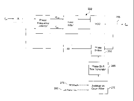
Fig. 1 illustrates a second-order phase-locked loop system.
Fig. 2 illustrates a phase-locked loop having a phase shifter according to
various embodiments of the invention.
Fig. 3 illustrates a phase shifter system according to various embodiments of
the invention.
5
CA 02612431 2007-12-13
WO 2007/005475
PCT/US2006/025213
DETAILED DESCRIPTION OF THE PREFERRED EMBODIMENTS
The present invention provides a system, apparatus and method for recovering
a client signal clock. The present invention is able to more effectively
remove jitter
within a clock signal by providing a phase shifting element in the feedback of
a PLL
system to compensate for sudden changes in an input reference clock. The PLL
system provides flexible clock recovery so that it can accommodate various
payload
types because it extracts a client clock signal independent of a corresponding
justification count number.
The following description is set forth for purpose of explanation in order to
provide an understanding of the invention. However, it is apparent that one
skilled in
the art will recognize that embodiments of the present invention, some of
which are
described below, may be incorporated into a number of different computing
systems
and devices. The embodiments of the present invention may be present in
hardware,
software or firmware. Structures and devices shown below in block diagram are
illustrative of exemplary embodiments of the invention and are meant to avoid
obscuring the invention. Furthermore, connections between components within
the
figures are not intended to be limited to direct connections. Rather, data
between
these components may be modified, re-formatted or otherwise changed by
intermediary components.
Reference in the specification to "one embodiment", "in one embodiment" or
"an embodiment" etc. means that a particular feature, structure,
characteristic, or
function described in connection with the embodiment is included in at least
one
embodiment of the invention. The appearances of the phrase "in one embodiment"
in
various places in the specification are not necessarily all referring to the
same
embodiment.
A. Overview
From the optical link of the end node, a digital wrapper of the client data is
received at a given carrier frequency, f
-carrier. The timing information associated with
the client signal can be extracted from the digital wrapper by scaling the
carrier
frequency and then subtracting that portion which is associated with the
justification
count, or JC. This concept can be mathematically expressed as follows:
6
CA 02612431 2014-02-13
WO 2Oc7/005475
1er/US2006/025213
(Fasõ,
"2.'" fainfer
1.101
Whom fp.a.r ;sew frequeney of the client signal;
other' frequency extracted from the digital meow,
is the number threw iii a It2lee 9fdatA
Ok. is the number of Other bytes in the frame of data; mid
./C.,s is the average justification court.
The Other bytes (Ow.) in equation (2) Mehra, overhead (OH), forward entr
correction (FEC) intimation and frame padding to create a desired frame OA,
otherwise referred ta as Staff bytes. For more detailed information regarding
the
digital' wrapper frame street= es dimmed herein, see U.S, Patent Application
1W715,947, filelbinvembec 18,2003, entitled *10ptitta1 Transmission Netwodt
with
Concluonons Mapping and Demapping and Digital Wrapper Frame for the Same,"
and MI Patent Application 11/15055, filed June 16,2005, entitled "tinivental
Digital Framer Architecture ibr Transport of Client Signals of Any Client
Payload and
Format Type".
Since the carrier frequency, &tune bytes and Other bytes are constant, the
equation cal be rewritten go iblborg:
foostme o,( 6) fori.H.rpc,) (3)
Thee, koin equation (3) above, One Oen see that the client or payload
/*pato is represented by the diftbrence of two terms, the first tenn equal to
the
cattier Eminency sealed by a factor related to the amount of COFFECIStuff
bytes
which exist and the total number of bytes in dm Mime. The second team is that
portion oldie cattier frequency associated with the JC of the frame sod
represents the
amount of phase shin which must mom in order tn recover the original client or
payload frequency. The ring tam of the above equation provides for a coarse
adjustment of the curler frequency to a value neer-the desired payload
frequency,
while the second term provides for fine erthastmenta of the coarse clock to
get the
actual value of the client or payload clock frogeoncy.
7
_
CA 02612431 2007-12-13
WO 2007/005475
PCT/US2006/025213
The above equation can be carried out by use of a conventional PLL system
with the addition of a phase shifter applied at its output, \Tout, the PLL
scaling the
carrier frequency while the phase shifter taking into account the JC of the
frame.
However, such a system is undesirable since the recovered clock may have a
high
incidence of jitter due to the phase shifter.
In accordance with the present invention, the phase shifter is operably placed
in the feedback loop of a conventional PLL circuit to recover the client
signal clock
from a digit'al wrapper frame while eliminating jitter associated with the
phase shifter
itself.
Now turning to Fig. 2, a new PLL system 200 in accordance with the present
invention will be discussed in greater detail. As shown, a phase shifter 260
is inserted
in the feedback loop of the PLL system 200. The recovered client clock is
phase
shifted according to the justification count information 280, as discussed
above, to
represent the clock rate of the effective payload being transported within the
digital
wrapper. In such a configuration, with the phase shifter output being feed
into the
phase detector of the PLL, the PLL acts as a jitter filter resulting in very
little jitter as
part of the client signal clock.
As stated above, the PLL locks onto a scaled factor of the carrier frequency.
While the scaled factor is discussed as being known or constant, or perhaps
programmable, it is important to note that these values can change from time
to time
by various governing bodies to support new frame definitions. For example, the
Stuff
bytes may be increased or decreased as appropriate to handle new frame size
limitations. Therefore, in accordance with the invention, the PLL system 200
of Fig.
2 handles the frequency conversion between the carrier frequency and the
client signal
frequency, and the filtering, or otherwise suppression, of jitter generated by
the phase
shifter 260. In order to adequately suppress jitter the PLL system 200 should
have
very low loop bandwidth and very low jitter generated by the PLL itself.
Each increment or decrement in the JC is associated with a certain number of
phase shift events depending on the resolution of the phase shifter 260. As
shown in
Fig. 2, the JC is filtered by a JC filter 270 so that the fluctuation of the
JC 280 from
frame to frame is averaged. The number of phase shift events from frame to
frame is
low-pass filtered. The phase shift tick generator 265 then evenly distributes
the phase
8
CA 02612431 2007-12-13
WO 2007/005475
PCT/US2006/025213
shift events within each frame, minimizing any sudden phase shift events which
could
lead to jitter or wander in the output fout 255. These two blocks are used to
make the
phase shifting as smooth as possible so that the residual jitter through the
PLL 200 is
minimized.
In a preferred embodiment, the phase shifter 260 itself is a quadrature phase
shifter which utilizes an internal 90 degree phase shifter to geneyate the in-
phase clock
(I-clock) and quadrature-phase clock (Q-clock). Preferable, the phase shifter
260
comprises 12-bit digital to analog (DAC) converters, providing a minimum phase
step
smaller than 1/1024 or a clock period, although any suitable DAC resolution
meeting
the requirements discussed herein may be used. For example, if the clock
frequency
is 155MHz, the resulting minimum phase shift step of a 12-bit DAC would be
around
6 ps. In any rate, the phase shift step should be small enough for the stable
operation
of the main PLL, without excessive jitter or wander.
While the phase shifter 260 is described as being a quadrature phase shifter,
any suitable phase shifter can be utilized as long as the phase shift step is
small
enough to minimize jitter. For example, a PLL-based phase shifter typically is
capable of generating a phase step of 1/16 or 1/32 of a clock period. If the
clock
frequency is 155 MHz, the resulting minimum phase step would be around 200 Ps.
This phase step might be too large for the main PLL system to handle with
regards to
jitter. A PLL-based phase shifter would be acceptable if the operating
frequency were
high enough such that the jitter was miriimized.
As discussed above, the JC value is averaged. The justification count filter
270 is used to average, or otherwise smooth out fluctuations of, JCs from
frame to
frame. The JC filter 270 internally accumulates a number K of distinct frames
of JC
information 280, defined as the JC of a "super frame." For example, with a
frame rate
of 21.26 kHz, providing a frame period of about 47.04 Rs, a super frame time
period
is defined as 47.04 * K Rs. The summation of previous L super frames is used
to
determine the total number of phase shift events needed for this super frame
period.
The super frame size K, should be chosen so that the super frame period is at
least longer than the time constant of the main PLL system. The number of
super
frames used in averaging, L, should be equal to the number of phase shift
steps that
will shift the clock by the amount equivalent to two bytes of payload data per
frame of
9
CA 02612431 2007-12-13
WO 2007/005475
PCT/US2006/025213
data. For example, if the PLL loop bandwidth is around 50 Hz, the super frame
size,
K, should be at least 512. The phase step number, L, has to be at least 1024
in order
to keep the phase step close to 6 ps. It is preferable to have L even larger
than 1024.
While the invention has been disclosed in terms of using the justification
value
to determine and provide a phase shift to the output of the main PLL to
recover a
client clock signal, other frame information can be included in such a
determination.
In this way, the digital wrapper acquisition system can react to its "overall
system
health" and manipulate the rate at which the phase shifter operates on the
output fout
255 of the PLL 200. For example, under certain circumstances wander may
accumulate in the system and, ultimately, must be absorbed by the demapping
framer
FIFO (not shown). In order to eliminate errors associated with FIFO overflow
or
underflow conditions, the FIFO depth information 275 can be applied as an
input to
the justification count filter as shown. In this way, if the FIFO depth 275 is
outside of
a programmable or desired operating range, the phase shifting can be
accelerated to
bring the FIFO depth 275 within operating range.
Now turning also to Fig. 3, a phase shifter system 300 in accordance with one
embodiment of the present invention is described in greater detail. Fig. 3
depicts the
system functional block diagram of the phase shifter, comprising an interface
to two
input signals and associated remapping electronics, a multiplexer 325, a
numerical
controlled oscillator ("NCO") 335 and an IQ modulator 340. As discussed above,
the
quadrature phase shifter takes the output from the main PLL and phase shifts
the
signal based upon the quadrature cosine and sine inputs and feeds the
resulting signal
back to the phase frequency detector or comparator of the PLL, as shown.
The source of a first of the two input signals is obtained from an integrated
circuit (IC) 310 and is based on the carrier frequency and JC count of the
current
frame, as part of the digital wrapper. To standardize the clock domains within
the
system, the signal is remapped by the JC remapper 315 to a new JC value,
JCnew, and
fed to the multiplexer 325. Such standardization may be unnecessary depending
on
the specific clock configuration requirements of the system. JCnew is
representative of
the amount of phase shift to apply to the PLL output to recover the client
clock.
The source of the second of the two input signals is an onboard reference
clock 305 which is then remapped using a REF remapper 320 to a new reference
CA 02612431 2007-12-13
WO 2007/005475
PCT/US2006/025213
signal Refiew, which is close in characteristics, however not necessarily
exact, to the
newly mapped JC signal discussed immediately above, and then fed as a second
input
to the multiplexer 325. The multiplexer 325 is then used to select one of the
two
signals for delivery to the digital filter 330 whose output controls the NCO
335
sinusoidal output which ultimately controls the IQ modulator 340.
In normal operation, the JCõ, signal is switched through the multiplexer 325
to the digital filter 330. As stated above, the remapped JC,,e, value is fed
to the digital
filter 330, which acts as a moving average filter to remove jitter and wander,
resulting
in an average JC value JCavg which is then used to drive the NCO 335. More
specifically, the JCaõg signal is fed to the NCO 335 which then outputs the
sinusoidal
signals to the IQ modulator 340 to achieve the desired phase shift. That is,
the
frequency of the NCO output will shift the input clock, fout, by the NCO
output
frequency. Thus, the justification count is utilized to calculate an offset
frequency
and the phase shifter rotates the fout clock signal to obtain a frequency
shift
corresponding to the offset frequency. This signal is then fed back to the
phase
frequency detector which drives the VCO output toward the desired client
signal
clock frequency.
However, if for some reason the JCnew signal cannot be accurately produced
due to degradation of one or more parameters used by the integrated circuit
310 which
provides the source of JCnew, or otherwise a synchronization failure of the
current data
frame has occurred, the system can switch the multiplexer input to the
reference
signal Refiew allowing the system to continue to acquire data while reacting
to and
correcting the JCnew calculation. It is important to note that the reference
signal Ref is
derived in the digital wrapper acquisition systems and, therefore, is always
present
and able to take the place of JCõew, whenever needed. Since the reference
signal is in a
standby mode and used only when the JCnew signal is unobtainable, the
reference
signal may be referred to as JCstandby=
It should be apparent to those skilled in the art that, while the invention
has
been described in terms of utilization of a phase shifting element in the
feedback loop
of the PLL, other suitable elements which perform the same end result as the
phase
shifting element may be employed. For example, a tunable signal generator may
be
operably placed within the feedback loop of the PLL, the programmable
generator
11
CA 02612431 2007-12-13
WO 2007/005475
PCT/US2006/025213
providing a desired output to the phase frequency detector representative of
the
desired frequency offset, as representative by the JC of the frame as
described herein,
which will result in the attainment of the client signal clock at the output
of the PLL.
In a still further example, the desired offset frequency derived above, which
the JC average part, which is the variable part of the formula, can be
provided to a
variable frequency generator which can directly generate the client signal
from the
offset part plus the Other bytes part of the formula, which is the constant
part of the
formula, to directly produce the client signal frequency. This embodiment will
significantly reduce the amount of circuitry required to accurately
reconstitute the
client clock signal compared to the principal embodiment discussed previously
in this
application. This approach in recovering the client clock without jitter is a
next
generation implementation.
The foregoing description of the invention has been described for purposes of
clarity and understanding. It is not intended to limit the invention to the
precise form
disclosed. Various modifications may be possible within the scope and
equivalence of
the appended claims.
12