Note: Descriptions are shown in the official language in which they were submitted.
CA 02612776 2007-12-19
WO 2007/002100 PCT/US2006/023998
PASSIVE ELECTRICAL ARTICLE
Background
A continuing trend in the electronics industry is the miniaturization of
electronic
circuits and a corresponding increase of the circuit element density of
electronic circuits.
On conventional printed circuit boards, a large fraction of the board surface
area is
occupied by surface-mounted passive electrical devices, such as resistors,
capacitors and
inductors. One way to increase the density of circuit elements in an
electronic circuit is to
remove passive devices from the surface of the circuit board, and embed or
integrate the
passive devices into the circuit board itself. This has the added advantage of
placing the
passive devices much closer to the active circuit components, thus reducing
electrical lead
length and lead inductance, improving circuit speed, and reducing signal
noise. Signal
noise can lead to signal integrity and electro-magnetic interference (EMI)
issues.
Embedding the passive components into the board can reduce the size, thickness
and
number of layers in the board, which can significantly reduce the cost of the
circuit board.
The reduction in board size and thickness, as well as the elimination of the
surface-
mounted components and their associated vias and solder joints, can provide a
significant
reduction in weight and improved reliability. Finally, as signal rise times,
frequencies and
current and board densities continue to increase, there is a need for improved
thermal
dissipation at the printed circuit board level. Thin embedded passive layers
can also
provide improved thermal dissipation.
Summary
One aspect of the present invention provides a passive electrical article. In
one
embodiment, the passive electrical article comprises a first electrically
conductive
substrate having a major surface and a second electrically conductive
substrate having a
major surface, the major surface of the second substrate facing the major
surface of the
first substrate. An electrically resistive layer is on at least one of the
major surface of the
first substrate and the major surface of the second substrate. An electrically
insulative
layer is between the first and second substrates and in contact with the
electrically resistive
layer. The insulative layer comprises a polymer having a thickness ranging
from about 1
m to about 20 m. The insulative layer has a substantially constant thickness.
1
CA 02612776 2007-12-19
WO 2007/002100 PCT/US2006/023998
Another aspect of the present invention provides a method for forming a
passive
electrical article. In one embodiment, the method comprises providing a
laminate
structure comprising a first electrically conductive substrate having a major
surface, a
second electrically conductive substrate having a major surface, the major
surface of the
second substrate facing the major surface of the first substrate, an
electrically resistive
layer on at least one of the major surface of the first substrate and the
major surface of the
second substrate, and an electrically insulative layer between the first and
second
substrates and in contact with the electrically resistive layer, the
insulative layer
comprising a polymer having a thickness ranging from about 1 m to about 20 m,
wherein the insulative layer has a substantially constant thickness. At least
one of the first
substrate, the second substrate, and the resistive layer is circuitized to
form at least one of
a resistor, a capacitor and an inductor.
Another aspect of the present invention provides a printed circuit having a
circuitized laminate structure embedded therein. In one embodiment, the
laminate
structure comprises a first electrically conductive substrate having a major
surface, a
second electrically conductive substrate having a major surface, the major
surface of the
second substrate facing the major surface of the first substrate, an
electrically resistive
1ayer on at least one of the major surface of the first substrate and the
major surface of the
second substrate, and an electrically insulative layer between the first and
second
substrates and in contact with the electrically resistive layer, the
insulative layer
comprising a polymer having a thickness ranging from about 1 m to about 20 m,
wherein
the insulative layer has a substantially constant thickness.
Brief Description of the Drawings
The present invention will be further explained with reference to the appended
Figures, wherein like structure is referred to by like numeral throughout the
several views,
wherein the thickness of layers is not necessarily to scale, and wherein:
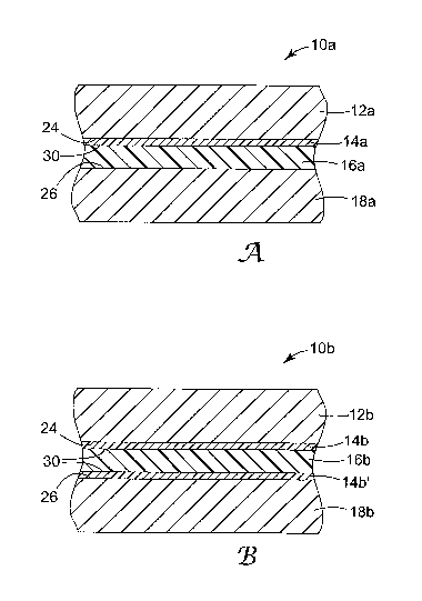
Figures 1 A- 1 C are cross-sectional views of a passive electrical article of
the
present invention, which can function as a capacitor, resistor, inductor, or
combination
thereof.
Figure 1 D is an expanded view of the electrically insulative layer in Figure
1 C.
2
CA 02612776 2007-12-19
WO 2007/002100 PCT/US2006/023998
Figures 2A through 2M illustrate an exemplary process for forming a resistor
using
a passive electrical article according to the present invention.
Figures 3A through 3E illustrate exemplary embodiments of a PCB having
embedded therein a passive electrical article according to the invention, in
which the
passive electrical article is patterned to function as a resistor (Figure 3A),
a capacitor
(Figures 3B and 3C), and an inductor (Figures 3D and 3E).
Figures 4A through 4F illustrate exemplary embodiments of a passive electrical
article having a single resistive layer according to one embodiment of the
invention, the
article patterned to function as a variety of combinations of passive
electrical elements.
Figures 5A through 5D illustrate exemplary embodiments of a passive electrical
article having two resistive layers according to one embodiment of the
invention, the
article patterned to function as a variety of combinations of passive
electrical elements.
Detailed Description
In the following Detailed Description, reference is made to the accompanying
drawings, which form a part hereof, and in which is shown by way of
illustration specific
embodiments in which the invention may be practiced. In this regard,
directional
terminology, such as "top," "bottom," "front," "back," "leading," "trailing,"
etc., is used
with reference to the orientation of the Figure(s) being described. Because
components of
embodiments of the present invention can be positioned in a number of
different
orientations, the directional terminology is used for purposes of illustration
and is in no
way limiting. It is to be understood that other embodiments may be utilized
and structural
or logical changes may be made without departing from the scope of the present
invention.
The following Detailed Description, therefore, is not to be taken in a
limiting sense, and
the scope of the present invention is defined by the appended claims.
The present invention is directed to a passive electrical article that can be
patterned
to function as a capacitor, resistor, inductor, or any combination thereof,
and which may
be embedded or integrated as a component of a circuit, for example, in a
printed circuit
board (PCB) or a flexible circuit (flexible circuits are a type of PCB). In
addition, the
passive electrical article itself, with some modifications, can function as an
electrical
circuit.
Passive Electrical Article
3
CA 02612776 2007-12-19
WO 2007/002100 PCT/US2006/023998
One embodiment of a passive electrical article of the present invention
comprises a
first electrically conductive substrate having a major surface, a second
electrically
conductive substrate having a major surface facing the major surface of the
first substrate,
an electrically resistive layer on at least one of the major surface of the
first substrate and
the major surface of the second substrate, and an electrically insulative
layer between the
first and second substrates and in contact with the electrically resistive
layer. The first
substrate, the second substrate, the resistive layer and the insulative layer
are selectively
patterned to form passive elements including capacitors, resistors, inductors,
and
combinations thereof. Potential applications for a passive electrical article
that functions
as a capacitor, resistor, inductor, or any combination thereof according to
the present
invention are varied, and the range of desired capacitance, resistance, and
inductance
varies according to the intended application.
Figures 1A-1C illustrate exemplary embodiments of a passive electrical article
10a,
,. .
10b, 10c, respectively, according to the present invention that may function
as a capacitor,
resistor, inductor, or any combination thereof. Referring to Figure 1A,
passive electrical
article i 0a comprises a laminate of first substrate 12a, electrically
resistive layer 14a,
electrically insulative layer 16a, and second substrate 18a. Referring to
Figure 1B, passive
electrical article 10b is constructed similarly to passive electrical article
10a, but includes
an additional electrically resistive layer in the laminate (that may be of a
different
resistivity), such that a resistive layer is positioned adjacent both
substrates. In particular,
passive electrical article 10b comprises first substrate 12b, electrically
resistive layer 14b,
electrically insulative layer 16b, second electrically resistive layer 14b',
and second
substrate 18b. Referring now to Figure 1 C, passive electrical article 10c is
constructed
similarly to passive electrical article 10a. In particular, passive electrical
article 10c
comprises first substrate 12c, electrically resistive layer 14c, electrically
insulative layer
16c, and second substrate 18c. Insulative layer 16c contains a plurality of
particles 20 in a
polymer 22, as shown in expanded Figure 1D. The particles 20 may or may not
contact
each other and may be arrayed in a predetermined manner, for example,
uniformly, or
randomly, depending on the desired end application. In one embodiment, the
particles 20
are substantially spherical in shape, and in another embodiment the particles
20 have
other, non-spherical shapes. In one embodiment, the particles 20 have a
regular shape and
size, and in another embodiment the particles 20 have irregular shapes and/or
sizes.
4
CA 02612776 2007-12-19
WO 2007/002100 PCT/US2006/023998
For purposes of clarity and ease of description, unless otherwise specifically
noted,
passive electrical articles 10a, lOb, lOc, first substrates 12a, 12b, 12c,
resistive layers 14a,
14b, 14b', 14c, insulative layers 16a, 16b, 16c, and second substrates 18a,
18b, 18c, will
be referred to herein generally as passive electrical article 10, first
substrate 12, resistive
layer(s) 14, insulative layer 16, and second substrate 18.
So that the passive electrical article 10 may function as a capacitor,
resistor,
inductor, or any combination thereof, first substrate 12 and second substrate
18 are
conductive. Alternately, at least a major surface 24 of first substrate 12 and
a major
surface 26 of second substrate 18 are conductive. The resistive layer 14 is
also electrically
conductive, but is less electrically conductive than the adjacent first or
second substrate
12, 18, respectively. The difference in electrical conductivity between first
and second
substrate 12, 18 and resistive layer 14 may result from differences in
material properties
and/or dimensions. In one embodiment, the second substrate 18 is not
originally included
in the lamination comprising the passive electrical article, and instead the
second substrate
comprises a layer of a printed circuit to which the passive electrical article
is joined. In
each of the embodiments of Figures lA-1C, insulative layer 16 has a
substantially constant
thicknesses. In one embodiment, each of the first substrate 12, second
substrate 18,
resistive layer 14 and insulative layer 16 have substantially constant
thicknesses.
In Figures 1A-1C, when the passive electrical article 10 is patterned to form
a
resistor, current flows through the resistive layer 14 in the plane of the
resistive layer 14.
Current input and output contact pads (not shown) are formed in first
substrate 12, and
current flows between the contact pads. If a resistive layer 14 is also
provided adjacent.
second substrate 18, a resistor may similarly be formed on the second side of
the article.
When the passive electrical article 10 is patterned to form a capacitor,
opposed capacitive
plates (not shown) are formed in first substrate 12 and second substrate 18.
In some
embodiments, resistive layer(s) 14, which are also conductive, but less so
than substrates
12, 18, may extend the capacitive plate beyond the edges of patterned
substrates 12, 18.
When the passive electrical article 10 is patterned to form an inductor, a
coiled structure
having input and output contacts (not shown) is formed in one or both of the
substrates 12,
18.
The layers of the passive electrical article 10 illustrated in Figures 1 A-1 C
are
resistant to separation, delamination, or cohesive failure. In one embodiment,
a force
5
CA 02612776 2007-12-19
WO 2007/002100 PCT/US2006/023998
required to separate the layers or induce cohesive failure of any of the
layers of the passive
electrical article 10 at a 90 degree peel angle is greater than about 3
pounds/inch (about 0.5
kiloNewtons/meter (kN/m)), preferably greater than 4 pounds/inch (0.7 kN/m),
more
preferably greater than 6 pounds/inch (1 kN/m), as measured according to the
IPC Test
Method Manual, IPC-TM-650, test number 2.4.9 dated October 1988, as published
by the
Institute for Interconnecting and Packaging Electronic Circuits. This force is
required to
separate any adjacent layers in the laminate comprising the passive electrical
article 10,
such as a substrate 12, 18 from an adjacent insulative layer 16, a substrate
12, 18 from an
adjacent resistive layer 14, or an insulative layer 16 from an adjacent
resistive layer 14 or
induce cohesive failure within the substrate 12, 18, the resistive layer 14 or
the insulative
layer 16.
In one embodiment, the article 10 has a capacitance density greater than about
1
nF/in2, preferably greater than about 4 nF/in2, more preferably greater than
about 10
nF/in2.
,,,15 Substrate
Substrates 12, 18 of the passive electrical article 10 may comprise a single
layer or
a plurality of layers, for example, a laminate. Substrates 12, 18 may comprise
graphite;
composites such as silver particles in a polymer matrix; metal such as copper
or
aluminum; combinations thereof, or laminates thereof. An example of a
multilayer
substrate includes copper on polyimide. The first and second substrates 12, 18
may be the
same or different in materials and construction.
In accordance with the present invention, at least one of the substrates 12,
18 is a
self-supporting substrate. As used herein, the term "self-supporting
substrate" refers to a
substrate having sufficient structural integrity such that the substrate is
capable of being
coated and handled without a carrier for support. It is preferable that
substrates 12, 18 are
flexible; however, rigid substrates may also be used. In one embodiment, the
substrates
12, 18 have a thickness ranging from approximately 5 to 80 m, more preferably
approximately 10 to 40 m. When the ability to spread high thermal loads or
handle high
currents is required, substrates having a thickness at the higher ranges are
preferred, such
as a thickness of at least approximately 70 m.
6
CA 02612776 2007-12-19
WO 2007/002100 PCT/US2006/023998
Typically, a major surface 24 of the first substrate 12 in contact with the
electrically resistive layer 14 is electrically conductive, and a major
surface 26 of the
second substrate 18 in contact with the electrically insulative layer 16 (in
Figure 1A) or the
electrically resistive layer 14 (in Figure 1B) is also electrically
conductive. Surface
treatment, which adds material to these major surfaces 24, 26 by, for example,
oxidation
or reaction with a coupling agent, for example, silanes terminated with
functional groups,
may be used to promote adhesion between adjacent layers. The resulting
material on the
major surfaces 24, 26 of the substrates 12, 18 themselves may not necessarily
be
conductive. Specifically, if the major surface is in contact with insulative
layer 16 (and
not a resistive layer 14), material on the major surface does not have to be
conductive,
because a capacitor can be formed provided the substrate itself is conductive.
In one embodiment, the major surfaces 24, 26 of the first and second
substrates 12,
18 have an average surface roughness ranging from about 10 nm to about 300 nm,
preferably 10 nm to 100 nm, more preferably 10 nm to 50 nm. If the
electrically insulative
layer 16 thickness is 1 m or less, the average surface roughness preferably
ranges from
10 nrn to 50 nm. Average surface roughness, RMS, is measured by taking the
square root
of the average, [(zl)a +(z2)2 +(z3)Z +...(zn)2]/n, where z is a distance above
or below the
substrate surface mean and n is the number of points measured and is at least
1000. The
area measured is at least 0.2 mm2. Preferably, no zn is greater than half the
thickness of
the electrically insulative or electrically resistive layer.
When the substrate is a metal, the metal preferably has an anneal temperature
which is at or below the temperature for curing the electrically insulative
layer 16, or the
metal is annealed before the electrically insulative layer 14 is coated.
A preferred substrate is copper. Exemplary copper includes copper foil
available
from Carl Schlenk, AG, Nurnberg, Germany, or from Olin Corporation's Somers
Thin
Strip/Brass Group, Waterbury, Connecticut.
Electrically Resistive Layer
The electrically resistive layer(s) 14 of the passive electrical article 10
comprises a
thin film of high-ohmic material. Exemplary high-ohmic materials include, but
are not
limited to, nickel-chromium (NiCr), nickel-chromium-aluminum-silicon
(NiCrAlSi),
nickel-pholsphorous (NiP), or doped conductive, such as doped platinum. In one
embodiment, the resistive layer(s) 14 are formed from a material having high
magnetic
7
CA 02612776 2007-12-19
WO 2007/002100 PCT/US2006/023998
penneability, such as a ferrite material, nickel-iron alloys such as
permalloy, silicon steel
or cobalt alloys. Materials with a relative permeability of greater than 10
are preferred and
those with a relative permeability of greater than 100 are more preferred to
provide greater
inductance when the passive article is patterned to form an inductor. In one
embodiment,
resistive layer(s) 14 have a thickness less than about 2 m. In one
embodiment, resistive
layer(s) 14 have a resistivity greater than about 25 Ohms/Sq, preferably
greater than about
250 Ohms/Sq., and more preferably greater than about 500 Ohms/Sq.
In one embodiment, the resistive layer(s) 14 are provided on one or both
substrates
12, 18 by sputtering, physical vapor deposition, chemical vapor deposition,
electroplating,
or any other suitable method known in the art which is suitable for the
particular materials
of the resistive layer(s) 14 and substrates 12, 18. Suitable resistive layers
on copper
substrates include copper substrates with integrated thin film resistor,
having the trade
designations TCR and TCR+ from Gould Electronics Inc., Chandler, Arizona;
INSITE
Embedded Resistors from Rohm & Haas Electronic Materials, Marlborough,
Massachusetts; and OHMEGA-PLY Resistor-Conductor Material from Ohmega
Technologies, Inc., Culver City, California.
The surface 30 of resistive layer(s) 14 that interfaces with insulative layer
16 will
have surface roughness characteristics similar to the major surfaces 24, 26 of
the first and
second substrates 12, 18 as described above. In particular, in one embodiment,
surface 30
has an average surface roughness ranging from about 10 nm to about 300 nm,
preferably
10 nm to 100 nm, more preferably 10 nm to 50 nm. If the electrically
insulative layer 16
thickness is 1 m or less, the average surface roughness preferably ranges
from 10 nm to
50 nm. Average surface roughness, RMS, is measured as described above.
Electrically Insulative Layer
The electrically insulative layer 16 of the passive electrical article 10,
which may
itself comprise one or more layers, comprises a polymer. Preferably, the
electrically
insulative layer 16 comprises a polymer and a plurality of particles and is
prepared from a
blend of resin and particles.
The electrically insulative layer 16, with regard to the surface roughness of
substrate material 12, 18 and resistive layer(s) 14, is selected to provide a
passive
electrical article that requires a force as described above to separate
adjacent layers (i.e., a
substrate or a resistive layer) from the insulative layer 16.
8
CA 02612776 2007-12-19
WO 2007/002100 PCT/US2006/023998
Suitable resins for the electrically insulative layer 16 include epoxy,
polyimide,
polyvinylidene fluoride, cyanoethyl pullulan, benzocyclobutene, polynorbomene,
polytetrafluoroethylene, acrylates, polyphenylene oxide (PPO), cyanate ester,
bismaleimide triazine (BT), allylated polyphenylene ether (APPE), and blends
thereof.
The organic polymers described in U.S. Patent Publication No. 2004/0222412,
commonly
assigned herewith and incorporated by reference in its entirety, are further
examples of
suitable materials for insulative layer 16,
Commercially available epoxies include those available from Resolution
Performance Products, Houston, Texas, under the trade designation EPON 1001F
and
EPON 1050. Preferably, the resin can withstand a temperature that would be
encountered
in a typical solder reflow operation, for example, in the range of about 180
to about 290 C.
These resins may be dried or cured to form the electrically insulative or
electrically
conducting layer.
Exemplary blends include blends of epoxies, preferably a blend of a
diglycidylether of bisphenol A and a novolac epoxy, for example, 90 to 70 % by
weight
EPON 1001F and 10 to 30 % by weight EPON 1050 based on the total weight of the
resin.
When particles are present, the particles are dielectric (or insulative)
particles or
conductive particles or mixtures thereof. Particle distribution may be random
or ordered.
Typically, particles in the insulative layer comprise dielectric or insulative
particles.
However, mixtures of particles are suitable provided that the overall effect
of the resin and
particle blend is insulative.
Exemplary dielectric or insulative particles include barium titanate, barium
strontium titanate, titanium oxide, lead zirconium titanate, and mixtures
thereof. A
commercially available barium titanate is available from Nippon Chemical
Industrial Co.,
Tokyo, Japan, under the trade designation AKBT.
The particles may be any shape and may be regularly or irregularly shaped.
Exemplary shapes include spheres, platelets, cubes, needles, oblate,
spheroids, pyramids,
prisms, flakes, rods, plates, fibers, chips, whiskers, and mixtures thereof.
The particle size, i.e., the smallest dimension of the particle, typically
ranges from
about 0.05 to about 10 m, preferably 0.05 to 5 m, more preferably 0.05 to 2
m.
Preferably, the particles have a size allowing at least two to three particles
to be stacked
vertically within the electrically insulative layer thickness. A relatively
large particle
9
CA 02612776 2007-12-19
WO 2007/002100 PCT/US2006/023998
having a particle size slightly larger than the thickness of the electrically
insulative layer
undesirably allows individual particles to bridge the gap between layers on
either side of
the insulative layer. During lamination, these relatively large particles will
cause a
compressive force leading to surface deformation and a "wiping" action at the
particle-
substrate interface or the particle-resistive layer interface, which may
remove surface
oxide layers.
The loading of particles in the polymer is typically 20 to 70 % by volume,
preferably 30 to 60 % by volume, more preferably 40 to 50 % by volume, based
on the
total volume of the electrically insulative layer.
In one embodiment, the thickness of the electrically insulative layer 16
(comprising one or more layers) ranges from about 1 to about 20 m. In another
embodiment, the thickness of the electrically insulative layer 16 ranges from
about 8 to
about 16 m.
In one embodiment, the dielectric constant of the insulative layer 16 is
greater than
about 4, preferably greater than about 11, more preferably greater than about
15.
In one embodiment, the insulative layer 16 has a thermal conductivity greater
than
about 0.2 W/m-K, preferably greater than about 0.35 W/m-K, more preferably
greater than
about 0.5 W/m-K.
Method of Manufacturing a Passive Electrical Article
A method for manufacturing a passive electrical article 10 in accordance with
the
present invention comprises providing a first substrate 12 having a major
surface 24
substantially, free of debris or chemisorbed or adsorbed materials, and
providing a resistive
layer 14 on at least the major surface 24 of first substrate 12. The resistive
layer 14 may
be provided on the major surface 24 by sputtering, physical or chemical vapor
deposition,
electroplating, or any other suitable method known in the art. A blend
comprising a resin
is provided and coated onto the surface 30 of the resistive layer 14, and a
major surface 26
of a second substrate 18 is laminated to the blend. The blend is then cured or
dried.
Alternatively, the blend may be coated on the major surface 26 of the second
substrate 18,
and the blend-coated surface 26 of the second substrate 18 laminated to the
surface 30 of
the resistive layer 14 on the first substrate 12. Alternatively, the blend may
be coated on
the surface 30 of resistive layer 14 and on the major surface 26 of the second
substrate 18,
and the blend-coated surfaces 30, 26 laminated together. It will be recognized
that the
CA 02612776 2007-12-19
WO 2007/002100 PCT/US2006/023998
above method for manufacturing a passive electrical article 10 results in the
embodiment
illustrated in Figure 1 C. In other embodiments, a resistive layer 14 can also
be provided
on the major surface 26 of second substrate 18, and/or a different material
may be used to
form insulative layer 16, so as to form the passive electrical article of
Figures 1A or 1B.
The substrates 12, 18 are preferably substantially free of debris or
chemisorbed or
adsorbed materials in order to maximize adhesion with the electrically
resistive layer 14
and the electrically insulative layer 16. This is achieved, for example, by
reducing the
amount of residual organics on the substrate surfaces 24, 26 and removing
debris from the
substrate surface 24, 26. Exemplary methods include surface treatment as
described
below. ~
The steps of the present invention are described in additional detail with
reference
to copper foil as the first and second substrates 12, 18, a doped platinum as
the resistive
layer 14, and electrically insulative layer 16 formed from epoxy and barium
tita.nate
particles.
A copper foil is provided for the first and second substrates 12, 18. The
copper foil
of the first substrate 12 is previously coated with a doped platinum resistor
layer 14
(INSITE Resistor Material from Rohm & Haas Electronic Materials, Marlborough,
Massachusetts). The copper foil substrates 12, 18 and doped platinum resistive
layer 14,
which may have material present on their exposed surfaces such as an organic
anti-
corrosion agent (for example, a benzotriazole derivative) and/or residual oils
from the
rolling process, are subjected to a surface treatment, for example, to ensure
good adhesion
between the electrically insulative layer 16 and the surface 30 of doped
platinum resistive
layer 14 on the first copper foil substrate 12, and also between the
insulative layer 16 and
the surface 26 of the second copper foil substrate 18. Removal can be effected
by, for
example, treating the copper foil substrate and/or doped platinum resistor
layer with an
argon-oxygen plasma or with an air corona, or wet chemical treatment can be
used as is
well understood in the art. Particulates adhering to the exposed surfaces of
the copper foil
substrates and doped platinum resistive layer can be removed using, for
example, an
ultrasonic/vacuum web cleaning device commercially available from Web Systems
Inc.,
Boulder, CO, under the trade designation ULTRACLEANER. Preferably, the copper
foils
and resistive layer are not scratched, dented, or bent during this surface
treatment step in
11
CA 02612776 2007-12-19
WO 2007/002100 PCT/US2006/023998
order to avoid possible coating problems and coating defects which may result
in non-
uniform coating or shorted articles, such as shorted capacitors.
The blend to be used for insulative layer 16 may be prepared by providing a
resin
such as epoxy, optionally a plurality of dielectric or insulative particles
such a barium
titanate, and optionally a catalyst. Adsorbed water or residual materials on
the particles;
e.g., carbonates, resulting from the manufacturing process can be removed from
the
surface of the particles before use. Removal may be accomplished by heating
the particles
in air at a particular temperature for a certain period of time, for example,
350 C for 15
hours. After heating, the particles may be stored in a dessicator before use
in the blend.
The blend of barium titanate particles and epoxy may be prepared as follows.
Barium titanate particles are first mixed with a ketone solvent containing a
dispersant.
Common mixing equipment can be a propeller stirrer. The weight ratios of
components
are typically 85% barium titanate, 13.5% solvent, and 1.5% dispersant. To
complete the
dispersion and break agglomerates, the mixture can be milled with a
homogenizer such as
a Gaulin homogenizer sold by APV, Lake Mills, WI. The concentrated dispersion
is
filtered to remove undispersed particles. Typically, the final filter in the
series is a 10
micron absolute filter. This filtered, concentrated dispersion can
subsequently be blended
with epoxy polymer solutions and other additives to produce a dispersion blend
suitable
for coating. Preferably, the final coating dispersion is filtered again just
prior to the
coating operation.
The blend may contain additives such as a dispersant, preferably a nonionic
dispersant, and solvents. Examples of dispersants include, for example, a
copolymer of
polyester and polyamine, commercially available from Avecia Pigments &
Additives,
Manchester, UK under the trade designation SOLSPERSE 24000. Examples of
solvents,
for example, include methyl ethyl ketone and methyl isobutyl ketone, both of
which are
commercially available from Aldrich Chemical, Milwaukee, WI. In the preferred
system,
other additives are not required; however, additional components such as
agents to change
viscosity or to produce a level coating can be used.
A catalyst or curing agent may be added to the blend. If a catalyst or curing
agent
is used, the catalyst or curing agent can be added before the coating step.
Preferably, the
catalyst or curing agent is added just before the coating step.
12
CA 02612776 2007-12-19
WO 2007/002100 PCT/US2006/023998
Exemplary catalysts include amines and imidazoles. If particles having a basic
surface, i.e., having a pH of greater than 7, are not present, then exemplary
catalysts can
include those producing acidic species, i.e., having a pH of less than 7, such
as sulfonium
salts. A commercially available catalyst is 2,4,6-
tris(dimethylaminomethyl)phenol
commercially available from Aldrich Chemical Milwaukee, WI. Typically, a
catalyst is
used in an amount ranging from about 0.5 to about 8 % by weight, preferably
0.5 to 1.5 %,
based on the weight of resin. When 2,4,6-tris(dimethylaminomethyl)phenol is
used, the %
by weight based on the weight of resin is preferably 0.5 to 1 %.
Exemplary curing agents include polyamines, polyamides, polyphenols and
derivatives thereof. A commercially available curing agent is 1,3-
phenylenediamine,
commercially available from E. I. DuPont de Nemours Company, Wilmington, DE.
Typically, a curing agent is used in an amount ranging from about 10 to about
100 % by
weight, preferably 10 to 50 % by weight, based on the weight of resin.
The surface 30 of cleaned doped platinum resistive layer 14 and the surface 26
of
cleaned copper foil substrate 18 are coated with the blend using any suitable
method, for
example, a gravure coater. Preferably, coating is performed in a cleanroom to
minimize
contamination. The dry thickness of the coating depends on the percent solids
in the
blend, the relative speeds of the gravure roll and the coating substrate, and
on the cell
volume of the gravure used. Typically, to achieve a dry thickness in the range
of about 0.5
to about 10 m, the percent solids are in the range of 20 to 60 % by weight.
The coating is
dried to a tack-free state in the oven of the coater, typically at a
temperature of less than
about 100 C, preferably the coating is dried in stages starting with a
temperature of about
C and ending with a temperature of about 100 C, and then wound onto a roll.
Higher
final drying temperatures, e.g., up to about 200 C can be used, but are not
required.
25 Generally, very little cross-linking occurs during the drying step; its
purpose is primarily
to remove as much solvent as possible. Retained solvent may lead to blocking
(i.e.,
unwanted interlayer adhesion) when the coating is stored on a roll and to poor
adhesion for
the laminate.
Coating techniques to avoid defects include in-line filtration and deaeration
(to
30 remove air bubbles) of the coating mixture. In one implementation, before
laminating two
substrates coated with an electrically insulative layer, at least one of the
electrically
insulative layers is partially cured, preferably in air, if a resin requiring
curing is used. In
13
CA 02612776 2007-12-19
WO 2007/002100 PCT/US2006/023998
particular, adhesion of the substrate may be improved by heat treating the
coating before
lamination. The time for heat treatment is preferably short, for example, less
than about
minutes, particularly at higher temperatures.
Lamination of the electrically insulative layer coated surfaces 26, 30 is
carried out
5 by sending one or both of the substrates 12, 18 with insulative coating
thereon through an
oven before reaching the laminator, for example, at a temperature ranging from
about 5 to
25 C below the lamination temperature. Preferably, the electrically insulative
layer should
not touch anything during lamination and lamination should be done in a
cleanroom. To
make a passive electrical article of the present invention, the coated
substrates are
10 laminated, electrically insulative layer to electrically insulative layer,
using a laminator
with two nip rollers heated to a temperature ranging from about 150 to about
200 C,
preferably about 150 C. Suitable air pressure is supplied to the laminator
rolls, preferably
at a pressure ranging from 5 to 40 psi (34 to 280 kPa), preferably 15 psi (100
kPa). The
roller speed can be set at any suitable value and preferably ranges from 12 to
72
inches/minute (0.5 to 3.0 cm/second), more preferably 15 to 36 inches/minute
(0.64 to 1.5
cm/second). This process can be conducted in a batch mode as well.
The laminated material can be cut into sheets of the desired length or wound
onto a
suitable core. Once lamination is complete, the preferred cleanroom facilities
are no
longer required.
When the resin requires curing, the laminated material is then cured.
Exemplary
curing temperatures include temperatures ranging from about 140 to about 200
C,
preferably 160 to 190 C and exemplary curing times include a period ranging
from about
60 to about 180 minutes, preferably 60 to 100 minutes.
Adhesion of the electrically' insulative layer 16 to surface 30 of doped
platinum
resistive layer 14 and surface 26 of copper foil 18 may be enhanced if the
metal is
sufficiently soft at the time of coating or becomes soft during lamination
and/or cure; i.e.,
the foil and/or resistive layer is annealed before coating or becomes annealed
during
subsequent processing. Annealing may be accomplished by heating before the
coating
step or as a result of the curing or drying step if the metal anneal
temperature is at or lower
than the cure temperature of the resin. It is preferred to use a metal
substrate with an
anneal temperature below the temperature at which curing or drying and
lamination occur.
Annealing conditions will vary depending on the metal substrate used.
Preferably, in the
14
CA 02612776 2007-12-19
WO 2007/002100 PCT/US2006/023998
case of copper, at either of these stages in the process, the metal substrate
obtains a
Vickers hardness, using a 10 g load, of less than about 75 kg/mm2. A preferred
temperature range for copper to achieve this hardness ranges from about 100 to
about
180 C, more preferably 120 to 160 C.
Although a passive electrical article of the present invention can be
functional as it
is fabricated, the passive electrical article may preferably be patterned as
described below,
for example, to form discrete islands or removed regions in order to limit
lateral
conductivity. The patterned passive electrical article may be used as a
circuit article itself
or as a component in a circuit article, as described below.
Patterning
Resistor, capacitor and inductor elements can be created by patterning first
substrate 12, second substrate 18 or resistive layer 14. Other features such
as circuit traces
inchiding those that connect resistor, capacitor or inductive elements,
through hole contact
pads and through hole clearances (where no electrical connection is desired)
can also be
created by patterning first substrate 12, second substrate 18, resistive layer
14 or insulative
layer 16. It should be noted that the use of the phrase "through hole" is
being used as a
general term to include all vertical interconnect geometries such as through
holes, buried
vias and blind vias for example.
Any suitable patterning technique known in the art may be employed. For
example, patterning of the passive electrical article may be performed by
photolithography
and/or by laser ablation as is well known in the art.
Photolithography of the substrates 12, 18 may be performed by applying a
photoresist to the passive electrical article, which is then exposed and
developed to form a
pattern of concealed and exposed substrate areas on the passive electrical
article. If the
passive electrical article is then exposed to a solution known to chemically
attack or etch
the substrate, selected areas of the substrate can be removed. A stripping
agent, such as
potassium hydroxide, is then employed to remove the remaining areas of
photoresist. This
process allows areas of substrate to be removed that are not desired in the
circuit structure.
In areas where the substrate 12 and resistive layer 14 are both to be removed,
the
resistive layer 14 can be etched immediately after substrate 12 if desired.
For some
resistive materials, it will be possible to use the same etchant for substrate
layer 12 and
resistive layer 14.
CA 02612776 2007-12-19
WO 2007/002100 PCT/US2006/023998
An identical or similar photolighography process may be performed to pattern
resistive layer 14. Photolithography of the resistive layer 14 may be
performed by
applying a photoresist to the passive electrical article already having a
portion of resistive
layer 14 exposed (such as by photolithography of the substrate 12). This
process allows
areas of resistive layer to be removed that are not desired in the circuit
structure.
Preferably, substrates 12, 18 and resistive layer 14 are selectively etched.
That is, the
solution used to etch substrates 12, 18 does not etch resistive layer 14, and
the solution
used to etch resistive layer 14 does not etch substrates 12, 18.
Laser ablation may be performed by using a laser to selectively thermally
remove
material from any or all of the layers of the passive electrical article.
Photolithography
and laser ablation may be used in combination.
The thickness of the electrically insulative layer 16 may limit how the
passive
electrical article of the present invention can be patterned because the
insulative layer 16
itself may not mechanically support the substrates 12, 18. The electrodes may
be
patterned into substrates 12, 18 such that at least one of the substrates 12,
18 will always
support the passive electrical article. The first substrate 12 of the passive
electrical article
may be patterned and the second substrate 18 may remain continuous (or
unpatterned) so
that the passive electrical article has "structural integrity", i.e., the
article is capable of
being handled without a carrier for support and remains free-standing.
Typically, the
passive electrical article is double patterned, i.e., patterned on both sides,
without the use
of a support, provided the passive electrical article has structural
integrity.
Figures 2A-2M illustrate steps in an exemplary photolithography process for
forming a resistor from the passive electrical article 10 as illustrated in
Figures 1 A or 1 C.
A passive electrical article 10 comprising a laminate of first conductive
substrate 12,
electrically resistive layer 14, electrically insulative layer 16, and second
conductive
substrate 18 is provided (Fig. 2A), and a photoresist 40 is applied to the
conductive
substrates 12, 18 (Fig. 2B). Selected portions of the photoresist 40 are
exposed, such as by
exposure to ultraviolet light (Fig. 2C), and the photoresist 40 is developed
to remove the
unexposed portions 42 of the photoresist (Fig. 2D). A first etching solution
is used to etch
the revealed portions of conductive layers 12, 18 (Fig. 2E), and a second
etching solution
is used to etch revealed portions of resistive layer 14 (Fig. 2F). However, it
should be
noted that for some resistive materials, the same etchant can be used for both
the
16
CA 02612776 2007-12-19
WO 2007/002100 PCT/US2006/023998
conductor and resistive material. The photoresist 40 is stripped from the
article (Fig. 2G),
and a new layer of photoresist 44 is applied to the now revealed surfaces
(Fig. 2H). The
new layer of photoresist 44 is selectively exposed (Fig. 21), and the
photoresist 44 is
developed to remove the unexposed portions 46 of the photoresist (Fig. 2J).
The revealed
portions of conductive substrates 12, 18 are etched (in the example, only
portions of
substrate 12 are revealed) to define two separate electrodes 48, 50 (Fig. 2K),
and the
photoresist is again stripped (Fig. 2L). A resistor 52 is now defined between
electrodes
48, 50 in conductive substrate 12. Finally, the patterned article having
resistor 52 is
laminated into a printed circuit 54, such as a printed circuit board (Fig.
2M). The
conductive substrates 12, 18 of the article 10 are insulated from conductive
layers 56, 58
of the printed circuit board 54 by dielectric material 60. Electrodes 48, 50
may be
selectively connected to conductive layers 56, 58 by conductive vias (not
shown), as is
known in the art.
It should be noted that Figs. 2E and 2F, in which the conductive substrate
layers
12, 18 and resistive layer 14 are etched, respectively, could in another
embodiment, be
switched with Fig. 2K, in which conductive substrate layers 12, 18 are etched.
Additional
steps (such as cleaning to promote resist adhesion, baking to remove moisture,
providing a
copper surface treatment to improve the outside conductor surface to the
adjoining
dielectric, etc. can also be performed at appropriate locations in the
process. Different
types of passive electrical devices, including capacitors, resistors,
inductors and
combinations thereof may be formed using similar techniques. Additionally,
processes
such as laser trimming can be performed if precise tolerances are required for
the resistor.
Circuit Article
The passive electrical article of the present invention itself may function as
a
circuit article, with some modification. In one instance, the passive
electrical article 10
may be patterned. In this instance, a circuit article may be prepared by
providing a passive
electrical article 10 of the present invention and patterning the passive
electrical article 10
as described above to provide a contact for electrical connection. Either one
or both
substrates 12, 18 of the passive electrical article 10 are patterned to allow
access to each
surface of the first and second substrates 12, 18, and to provide a through-
hole contact.
In another embodiment, a circuit article may be prepared by a method
comprising
the steps of providing a passive electrical article 10 of the present
invention, providing at
17
CA 02612776 2007-12-19
WO 2007/002100 PCT/US2006/023998
least one electrical contact, and connecting the contact to at least one
substrate 12, 18 of
the passive electrical article 10.
A passive electrical article of the present invention may further comprise one
or
more additional layers, for example, to prepare a printed circuit board or
flexible circuit.
The additional layer(s) may be rigid or flexible. Exemplary rigid layers
include
fiberglass/epoxy composite commercially available from Polyclad, Franklin, NH,
under
the trade designation PCL-FR-226, ceramic, metal, or combinations thereof.
Exemplary
flexible layers comprise a polymer film such as polyimide or polyester, metal
foils, or
combinations thereof. Polyimide is commercially available from E.I. DuPont de
Nemours
Company, Wilmington, DE, under the trade designation KAPTON and polyester is
commercially available from 3M Company, St. Paul, Minnesota, under the trade
designation SCOTCHPAR. These additional layers may also contain electrically
conductive traces on top of the layer or embedded within the layer. The term
"electrically
conductive traces" refers to strips or patterns of a conductive material
designed to carry
current. Examples of suitable materials for an electrically conductive trace
include
copper, aluminum, tin solder, silver paste, gold, and combinations thereof.
In this embodiment, a preferred method of making a circuit article comprises
the
steps of providing a passive electrical article of the present invention,
patterning at least
one substrate 12, 18 of the passive electrical article, providing an
additional layer,
attaching the layer to the passive electrical article 10, and providing at
least one electrical
contact to at least one substrate 12, 18 of the passive electrical article.
Preferably, a
second additional layer is provided and attached to the passive electrical
article.
Printed Wiring Boards and Flexible Circuits
A passive electrical article of the present invention can be used in a printed
circuit
board or a flexible circuit, as a component, which functions as a capacitor, a
resistor, an
inductor, or any combination thereof. The passive electrical article may be
embedded or
integrated in the printed circuit board or flexible circuit.
A PCB typically comprises two layers of material, for example, a laminate of
epoxy and fiberglass, which may have one or, two copper surfaces, sandwiching
a layer of
adhesive or prepreg (the layer of prepreg can have more than one prepreg
"layer"). A
flexible circuit typically comprises a flexible layer, for example, a
polyimide layer coated
with copper, and a layer of adhesive on the polyimide. The position of a
passive electrical
18
CA 02612776 2007-12-19
WO 2007/002100 PCT/US2006/023998
article of the present invention in any suitable PCB or flexible circuit and
the process of
embedding or integrating a passive electrical article of the present invention
in any
suitable PCB or flexible circuit are well understood in the art. Notably, with
either a PCB
or flexible circuit, care must be taken to align the ' PCB or flexible circuit
layers/components.
As noted above, the thickness of the electrically insulative layer 16 may
determine
how the article 10 can be patterned. When the passive electrical article 10 is
incorporated
in a PCB or flexible circuit, the PCB or flexible circuit layers may lend
further support to
the passive electrical article allowing for additional unique patterning
techniques.
For example, a double patterning and lamination process may be useful. The
double patterning and lamination process comprises the following steps that
can occur
after the photolithographic patterning one of the substrates 12, 18 as
described above. In
this process, the patterned substrate is laminated to a supportive material
such as a circuit
board layer, for example, FR4, with the patterned side facing the supportive
material. The
other substrate can be patterned by an essentially similar technique, since
the electrically
insulative layer 16 and the patterned substrates are now fully supported by
the supportive
material. A second lamination on the exposed side of the second substrate is
then
conducted to complete the process.
Figures 3A-5D illustrate examples of the passive electrical articles of
Figures 1A -
1 C patterned to form capacitors, resistors, inductors, and various
combinations thereof.
Figures 3A through 3C illustrate examples of a PCB 100a, 100b, 100c,
respectively, having embedded therein a patterned passive electrical article
of Figure 1A
or 1C, in which a single resistive layer 14 is provided. PCB l 00a, l 00b, I
OOc, each
comprise two layers 102 of a material such as epoxy/fiberglass sandwiching
layers 104 of
insulative adhesive or prepreg, and a passive electrical article 10 of the
present invention,
which functions as a resistor in Figure 3A, a capacitor in Figure 3B, and an
inductor in
Figure 3C. The embodiments of Figures 3A-3D are illustrative only, and not
intended to
be limiting. In other embodiments, for example, one or both of layers 102 may
be
omitted.
Figure 3A illustrates PCB 100a containing a passive electrical article 10 of
the
present invention, which functions as a resistor. In Figure 3A, signals or
current are
routed through PCB 100a by through-holes 110 and 110', which are made
conductive by,
19
CA 02612776 2007-12-19
WO 2007/002100 PCT/US2006/023998
for example, electroplating with copper to form surface copper structures 112
and 112',
respectively. Surface copper structures 112, 112' route signals between
conductive traces
(not shown) on either upper surface 114 or lower surface 116 of PCB 100a.
First and
second substrates 12, 18 and resistive layer 14 are patterned to form pads 118
and 118'
that cover part of resistive layer 14. (Second substrate 18 has been
completely removed in
the illustrated area of the passive article 10). Pads 118, 118' are joined by
a portion 14' of
resistive layer 14. Surface copper structures 112, 112' are used to contact
pads 118, 118',
respectively, so that a controlled resistance can be measured between pads
118, 118',
based on the geometry (length and width) of the portion 14' of resistive layer
14 between
the two pads 118, 118', In other embodiments, different structures and method
for making
electrical connection with pads 118, 118' may be utilized, including, for
example, blind
conductive vias. In other embodiments, pads 118, 118' are electrically
connected to a
trace within the interior of the PCB. In other embodiments, layers 102, 104
comprise
flexible materials, such that the completed circuit article is flexible.
Figure 3B illustrates PCB 100b containing a passive electrical article 10 of
the
present invention, which iunctions as a capacitor. In Figure 3B, signals or
current are
routed through PCB 100b by vias 120 and 120', which are made conductive by,
for
example, filing the vias 120, 120' with a conductive material 122 or
electroplating, such as
with copper. Conductive vias 120, 120' route signals between conductive traces
(not
shown) on either upper surface 114 or lower surface 116 of PCB 100b. First and
second
substrates 12, 18 and resistive layer 14 are patterned to form capacitive
plates on either
side of insulative layer 16. In other embodiments, different structures and
method for
making electrical connection with pads conductive substrates 12, 18 may be
utilized. In
other embodiments, conductive substrates 12, 18 are electrically connected to
a trace
within the interior of the PCB. In other embodiments, layers 102, 104 comprise
a flexible
materials, such that the completed circuit article is flexible.
Figure 3C illustrates another embodiment of a passive electrical article 10 of
the
present invention, which functions as.a capacitor. In Figure 3C, signals or
current are
routed through PCB 100c by through-holes 110 and 110', which are made
conductive by,
for example, electroplating with copper to form surface copper structures 112
and 112',
respectively. Surface copper structures 112, 112' route signals between
conductive traces
(not shown) on either upper surface 114 or lower surface 116 of PCB 100c.
First and
CA 02612776 2007-12-19
WO 2007/002100 PCT/US2006/023998
second substrates 12, 18 and resistive layer 14 are patterned to form
capacitive plates
123a, 123b on either side of insulative layer 16. In other embodiments,
different structures
and method for making electrical connection with pads conductive substrates
12, 18 may
be utilized. In other embodiments, conductive substrates 12, 18 are
electrically connected
to a trace within the interior of the PCB. In other embodiments, layers 102,
104 comprise
a flexible materials, such that the completed circuit article is flexible.
Figures 3D and 3E illustrates PCB 100c containing a passive electrical article
10 of
the present invention, which functions as an inductor. In Figure 3D, signals
or current are
routed through PCB 100d by vias 120 and 120', which are made conductive by,
for
example, filing the vias 120, 120' with a conductive material 122 or
electroplating, such as
with copper. Conductive vias 120, 120' route signals between conductive traces
(not
shown) on either upper surface 114 or lower surface 116 of PCB 100d. First and
second
substrates 12, 18 and resistive layer 14 are patterned to form a coiled
inductive element on
one side of insulative layer 16 having contact pads 124, 124'. (Second
substrate 18 has
been completely removed in the illustrated area of the passive article 10). In
one
embodiment, resistive layer 14 is a high permeability material, such as a
ferrite material,
and is patterned to extend at least partially between the patterned coils of
conductive
substrate 12, such that the high permeability material is in the core of the
inductive coil,
thus providing a higher inductance for the inductor. In another embodiment,
the resistive
layer 14 has the same width as the conductive substrate 12. Conductive vias
120, 120'are
used to electrically connect with pads 124, 124', respectively. In other
embodiments,
different structures and method for making electrical connection with pads
124, 124' may
be utilized. In other embodiments, pads 124, 124' are electrically connected
to a trace
within the interior of the PCB. In other embodiments, layers 102, 104 comprise
a flexible
materials, such that the completed circuit article is flexible.
Figures 4A through 4F are illustrative examples of how a passive electrical
article
of Figure 1 A or 1C, in which a single resistive layer 14 is provided, can be
patterned to
provide a variety of electrical elements, and in particular a variety combined
passive
circuit elements. For purposes of clarity, the patterned articles are not
shown embedded in
a PCB or flexible circuit, as with Figures 3A-3C above. However, it is to be
understood
that the patterned articles of Figures 4A-4F are intended for such use.
21
CA 02612776 2007-12-19
WO 2007/002100 PCT/US2006/023998
Figure 4A illustrates a resistor in series with a capacitor. A resistive
element is
formed between conductive pads 130 and 132, as described with reference to
Figure 3A
above. A capacitive element formed between conductive pads 132 and 134, as
described
with reference to Figure 3B above.
Figure 4B illustrates another embodiment of a resistor in series with a
capacitor.
Both the resistive element and the capacitive element are formed between
conductive pads
136 and 138. Because the conductive pads 136, 138 are offset from each other,
the
resistive layer 14 (which is also conductive, but less conductive than
substrates 12, 18),
acts both as a resistive element, and also as an extension of the capacitive
plate of
conductive pad 136.
Figure 4C illustrates yet another resistive-capacitive structure. A resistive
element
is formed between conductive pads 140 and 142. The resistive material layer 14
forms
the top electrode for a capacitor, the bottom electrode of the capacitor being
conductive
pad 144.
Figure 4D illustrates an inductor in series with a resistor. An inductive
element is
formed between conductive pads 146, 148, and a resistive element is formed
between
conductive pads 148, 150.
Figure 4E illustrates an inductor in,series with a capacitor. An inductive
element is
formed between conductive pads 152, 154, and a capacitive element is formed
between
conductive pads 154, 156.
Figure 4F illustrates an inductor in series with a resistor and a capacitor.
An
inductive element is formed between conductive pads 158, 160, a resistive
element is
formed between conductive pads 160, 162, and a capacitive element is fonned
between
conductive pads 162 and 166. Resistive, capacitive and inductive elements can
also be
connected in parallel to each other if desired.
Figures 5A through 5D are illustrative examples of how a passive electrical
article
of Figure 1 B, in which a resistive layer 14 is provided on each substrate 12,
18, can be
patterned to provide a variety of electrical elements, and in particular a
variety of
combined passive circuit elements. For purposes of clarity, the patterned
articles are not
shown embedded in a PCB or flexible circuit, as with Figures 3A-3C above.
However, it
is to be understood that the patterned articles of Figures 5A-5D are intended
for such use.
22
CA 02612776 2007-12-19
WO 2007/002100 PCT/US2006/023998
Figure 5A illustrates an article having a resistor on both sides of insulative
layer
16. Separate resistive elements are formed between conductive pads 168, 170,
and
between conductive pads 172, 174. In this manner, a plurality of passive
elements may be
positioned within the same X-Y area of a printed circuit. These resistive
elements can be
electrically isolated from each other, or if desired, they can be connected in
series or
parallel to each other.
Figures 5B and 5C illustrate an article having an inductor on both sides of
insulative layer 16. Separate inductive elements are formed between conductive
pads 176,
178, and between conductive pads 180, 182. In the article of Figure 5C,
resistive layers
14, 14' are a high permeability material and extend between the coils of the
conductive
layers 12, 18, to provide higher inductance. The high permeability material of
resistive
layers 14, 14' can be either electrically connected to the conductive coils of
the inductor,
or electrically isolated from the conductive coils. For example, Figure 5C
illustrates the
high permeability material of layer 14 electrically connected to the
conductive coils of
layer 12, and the high permeability material of layer 14' electrically
isolated from the
conductive coils of layer 18.
Figure 5D illustrates a resistor in series with a capacitor. A resistive
element is
formed between conductive pads 184, 186, and a capacitive element is formed
between
conductive pads 186, 188.
The present invention also encompasses an electrical device comprising a
passive
electrical article of the present invention functioning as an electrical
circuit of a PCB or
flexible circuit, which comprises a passive electrical article in accordance
with the present
invention. The electrical device rimay include any electrical devices, which
typically
employs a PCB or flexible circuit having a capacitive or resistive component.
Exemplary
electrical devices include cell phones, telephones, fax machines, computers,
printers,
pagers, and other devices as recognized by one skilled in the art. The passive
electrical
article of the present invention is particularly useful in electrical devices
in which space is
at a premium.
This invention is illustrated by the following examples, but the particular
materials
and amounts thereof recited in these examples, as well as other conditions and
details
should not be construed to unduly limit this invention.
23
CA 02612776 2007-12-19
WO 2007/002100 PCT/US2006/023998
Example 1
A dispersion of 0.3 micron barium titanate in methyl ethyl ketone/methyl
isobutyl
ketone was prepared in a commercial bead mill using a polyester/polyamine
copolymer
dispersant. Sufficient epoxy binder solution (EPON 1001F plus EPON 1050) was
added
to give a volume ratio of barium titanate to epoxy of 45:55. The resulting
dispersion
(solids content of 60% w/w) was coated using a gravure coater onto 35 micron
(one
ounce) copper foil which had been previously coated with a <1 um doped
platinum
resistor layer, with a nominal resistivity of 1000 ohms per square, having the
trade
designation INSITE and obtained from Rohm & Haas Electronic Materials,
Marlborough,
Massachusetts. After drying, the barium titanate/epoxy layer was 5 to 6
microns thick. A
second sample of 35 micron copper foil, which had no resistor layer, was also
coated using
the same conditions. The two coatings were laminated, coated side to coated
side, in a roll
laminator set at approximately 135 C and 5.93x10⁻³ m/s (14 inches per minute
(ipm)).
The laminate was cured in an oven at 190 C for four hours.
The adhesion of the cured laminate was measured using a 90 degree peel test.
The
adhesion of the resistive material to the dielectric was at least 3.156 kN/m
(6 pounds per
linear inch (pli)). The adhesion of the resistive material to its copper
substrate was at least
3.156 kN/m (6 pli) as well, since the failure was at the resistive-dielectric
interface and not
at the resistive-copper interface. The adhesion of the dielectric to copper
was
approximately 1.578 kN/m (3 pli). The adhesion of the cured laminate was also
tested
after an additional 4 hour, 190 C thermal bake (to simulate two lamination
cycles in the
PCB process). There were no significant changes in adhesion for any of the
interfaces.
The electrical properties of the cured laminate were also tested. Capacitor
and
resistor structures were patterned into the conductive and resistive material
using
photolithographic methods well known in the art. The resistance and
capacitance were
measured on an LCR meter at 1 kHz frequency. The resistivity was found to be
approximately 1000 ohms per square on average. Thus, there was no significant
change in
resistivity due to the fabrication of the laminate or the patterning process.
The capacitance
was measured and found to be approximately 0.0155 nF/mm2 (10 nF/in2). The
change in
capacitance over the temperature range of 23 C to 180 C and back to 23 C was
also
measured. There was less than a 15% increase in capacitance over the 23 C to
180 C
range. When the sample was returned to 23 C, there was no net change in
capacitance.
24
CA 02612776 2007-12-19
WO 2007/002100 PCT/US2006/023998
Example 2
The same process and materials as above was used to coat a 5 to 6 um thick
dielectric layer on 35 um (one ounce) copper foil. Following this, two of
these layers were
laminated, coated side to coated side, in a hot roll laminator at
approximately 135 C and
5.93x10⁻³ m/s (14 ipm). One of the two copper foils was peeled away from the
laminated
structure which resulted in its dielectric coating being transferred to the
other dielectric
coated copper. The dielectric coated copper substrate (now with a dielectric
thickness of
approximately 10-11 um) was then laminated to an 18 um (one-half ounce) copper
foil
with a <1 um sputtered nickel-chromium resistive material (dielectric side
facing the
resistive material) with a sheet resistivity of 25 ohms per square. The copper
foil with
resistive material thereon was Gould TCR resistive conductor material
available from
Gould Electronics, Inc., Chandler, AZ. The laminate was cured at 190 C for
four hours.
The adhesion of the laminate was measured using a 90 degree peel angle. The
adhesion of the resistive material to the dielectric was found to be at least
3.156 kN/m (6
pli). As in Example 1, the adhesion of the resistive material to its copper
substrate was at
least 3.156 kN/m (6 pli) as well, since the failure was at the resistive-
dielectric interface
and not at the resistive-copper interface. The copper to dielectric adhesion
was found to
be approximately 2.104 kN/m (4 pli). The adhesion of the cured laminate was
also tested
after an additional 4 hour, 190 C thermal bake (to simulate two lamination
cycles in the
PCB process). There were no significant changes in adhesion for any of the
interfaces.
The electrical properties of the cured laminate were also tested. Capacitor
and
resistor structures were patterned into the conductive and resistive material
using
photolithographic methods well known in the art. The resistance and
capacitance were
measured on an LCR meter at 1 kHz frequency. The capacitance was measured to
be
about 0.0155 nF/mm2 (10 nF/in). The sheet resistivity of the laminate measured
to be
approximately 25 ohms per square.
Example 3
Dielectric material of the same formulation as in Examples 1 and 2 was coated
on
um (one ounce) copper foil using a similar process as stated in Examples 1 and
2, with
30 the exception that the thickness of the dielectric coating was
approximately 8 um. In this
case, the cured laminate was made by laminating and curing the dielectric
coated copper
CA 02612776 2007-12-19
WO 2007/002100 PCT/US2006/023998
foil and a 35 um copper foil with a <1 um thick, plated nickel-phosphorous
resistive
material (dielectric side facing resistive material) with a sheet resistivity
of 25 ohms per
square. The copper foil with resistive material thereon was OHMEGA-PLY
Resistive
Capacitive Material available from Ohmega Technologies, Inc., Culver City, CA.
The
laminate was cured at 177 C for two hours at temperature and at a pressure of
2.07x10⁶
N/m 6 (300 psi) in a vacuum lamination press.
Example 4
Dielectric material of the same formulation as Examples 1 and 2 was coated on
35
um (one ounce) copper foil using a similar process as stated in Examples 1 and
2, with the
exception that the thickness of the dielectric coating was approximately 4 um.
The
dielectric coated copper foil was laminated to the resistive coated copper
foil from
Example 3 (dielectric to resistor material) using a hot roll laminator at 135
C, a speed of
305 mm/m (12 ipm) and a roll pressure of 1.03x10⁵ N/ma (15 psi). The copper
foil which
was originally coated with 4 um thick dielectric was peeled away at an 180
degree angle
which transferred the dielectric layer from the copper foil to the resistive
surface. This
process was repeated on another sample to yield two 4 um thick dielectric
coated resistive-
conductor material sheets. These two sheets were then laminated dielectric to
dielectric to
yield a laminate with an 8 um thick dielectric and a resistive layer between
the dielectric
and each of the two copper foils. The laminate was then cured in an oven for
two hours at
180 C.
The adhesion of the laminate was measured using a 90 degree peel angle. The
adhesion of the resistive material to the dielectric was found to be
approximately at least
2.367 kN/m (4.5 pli). As in Example 1, the adhesion of the resistive material
to its copper
substrate was at least approximately 2.367 kN/m (4.5 pli) as well, since the
failure was at
the resistive-dielectric interface and not at the resistive-copper interface.
Although specific embodiments have been illustrated and described herein, it
will
be appreciated by those of ordinary skill in the art that a variety of
alternate and/or
equivalent implementations may be substituted for the specific embodiments
shown and
described without departing from the scope of the present invention. This
application is
intended to cover any adaptations or variations of the specific embodiments
discussed
herein. Therefore, it is intended that this invention be limited only by the
claims and the
equivalents thereof.
26