Note: Descriptions are shown in the official language in which they were submitted.
CA 02613344 2007-12-21
WO 2007/002326 PCT/US2006/024362
1
ELECTRONIC COIN RECOGNITION SYSTEM
BACKGROUND OF THE INVENTION
[0001] The present invention relates to a media recognition system and, more
particularly, to a media recognition system having an improved detection
system.
[0002] Media recognition systems have commonly been used to identify and/or
differentiate between various media including, for example, coins, chips,
tokens, etc. In the
past, media recognition systems employed mechanical and simple electronic
methods to
accept or reject media and differentiate between denominations of media. The
mechanical
and simple electronic methods that have been employed often lead to improper
acceptance of,
for example, foreign coins, false media, unwanted media denominations, metal
objects that
look like proper media, etc. There is a recent trend toward improving
operation of media
recognition systems. However, improvements in media recognition system
operation often
require large and expensive detection systems.
BRIEF DESCRIPTION OF THE INVENTION
[0003] Exemplary embodiments of the invention include a media recognition
system.
The media recognition system includes a sensing part and a media
discriminator. The
sensing part is disposed proximate to a media to be queried and produces a
sensing signal
responsive to the media. The sensing signal is a digital signal produced in a
single step by
the sensing part from an analog signal. The media discriminator receives the
sensing signal
from the sensing part to determine acceptability of the media.
[0004] Further exemplary embodiments of the invention include a media
recognition
system. The media recognition system includes a drop system, a sensing part
and a media
discriminator. The drop system inducing movement of media inserted into the
media
recognition system. The sensing part being disposed proximate to the drop
system and
producing a sensing signal responsive to the media. The sensing signal is a
digital signal
produced in a single step by the sensing part from an analog signal. The media
discriminator
receives the sensing signal from the sensing part to determine acceptability
of the media
CA 02613344 2007-12-21
WO 2007/002326 PCT/US2006/024362
2
[0005] The above, and other objects, features and advantages of the present
invention
will become apparent from the following description read in conjunction with
the
accompanying drawings, in which like reference numerals designate the same
elements.
BRIEF DESCRIPTION OF THE DRAWINGS
[0006] Referring now to the drawings wherein like elements are numbered alike
in
the several FIGURES:
[0007] FIG. 1 is a block diagram of an electronic media recognition system
according
to an exemplary embodiment;
[0008] FIG. 2 is a block diagram of a media sensing portion and a media
discriminator according to an exemplary embodiment; and
[0009] FIG. 3 shows an exemplary sensing path traced on a surface of a media.
DETAILED DESCRIPTION OF THE INVENTION
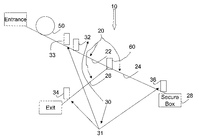
[0010] FIG. 1 shows a block diagram of an electronic media detection system
according to an exemplary embodiment. The electronic media detection system
(EMDS) 10
includes a drop system 20, an optional sensing part 30, and a media
discriminator 40. Media
50 which includes, for example, coins, tokens, chips, etc., are inserted iulto
the EMDS 10 via
the drop system 20. The sensing part 30 includes a media location
determination and
calibration portion 31 and a media sensing portion 32. The media sensing
portion 32
produces a sensing signal responsive to the media 50 and transmits the sensing
signal to the
media discriminator 40, which accepts or rejects the media 50 in response to
the sensing
signal.
[0011] Referring to FIG. 1, the drop system 20 includes a sensing path 22, a
vault
path 24, and a return path 26. The sensing, vault and return paths 22, 24 and
26 are each
tilted at a selected angle such that the media 50 rolls on an edge portion of
the media 50 while
passing through the drop system 20. In an exemplary embodiment the sensing,
vault and
return paths 22, 24 and 26 are each tilted at a pitch of about 12 degrees and
an angle of about
4 degrees over about 4 and %2 inches in order to slow a rolling speed of the
media 50.
CA 02613344 2007-12-21
WO 2007/002326 PCT/US2006/024362
3
[0012] The sensing path 22 is disposed from an entrance of the EMDS 10 to a
deflection gate 60. In an exemplary embodiment, the deflection gate 60 may be
a solenoid.
The deflection gate 60 includes an energized and a de-energized position. In
response to the
deflection gate 60 being in the de-energized position, the deflection gate 60
blocks access to
the vault path 24 and media 50 that is rolling down the sensing path 22 is
directed onto the
return path 26. In response to the deflection gate 60 being in the energized
position, the
deflection gate 60 allows access to the vault path 24 and the media that is
rolling down the
sensing path 22 continues from the sensing path 22 onto the vault path 24.
[0013] The vault pat1124 extends from the deflection gate 60 to a secure box
28. The
secure box 28 provides a volume to receive media that have been accepted by
the media
discriminator 40. The secure box 28 may be accessed by an operator to remove
stored media
from the secure box 28.
[0014] The return path 26 extends from the deflection gate 60 to an exit of
the EMDS
10. Since the deflection gate 60 directs media 50 down the return path 26 in
response to the
deflection gate 60 being in the de-energized position, the media 50 are
returned to an
individual who deposited the media 50 in the EMDS 10 in response to either the
media 50
being determined to be unacceptable or the EMDS 10 lacking power.
[0015] The media location determination and calibration portion 31 of the
sensing
part 30 may include at least one location sensor disposed proximate to the
drop system 20 so
that the sensor produces a location signal responsive to media 50 moving past
the sensor. In
an exemplary embodiment, as shown in FIG. 1, the media location determination
and
calibration portion 31 includes a media optical entrance detector (MOED) 33, a
media reject
optical detector (MROD) 34, and a media acceptance optical detector (MAOD) 36.
Although
FIG. 1 shows three location sensors, it should be noted that either more or
fewer location
sensors may be employed. The MOED 33 is disposed at a selected position along
the sensing
path 22. In an exemplary embodiment, the MOED 33 includes a transmitting
portion and a
receiving portion. The transmitting portion transmits an optical beain to the
receiving
portion. The transmitting and receiving portions may be disposed on opposite
sides of the
sensing path 22, such that the media 50 breaks the optical beam from the
transmitting portion
to the receiving portion for a time period. Alternatively, the transmitting
and receiving
CA 02613344 2007-12-21
WO 2007/002326 PCT/US2006/024362
4
portions may be disposed on a same side of the sensing path 22, such that the
media 50
reflects the optical beam from the transmitting portion to the receiving
portion. The time
period may be, for example, about 20 to about 30 milliseconds. Outputs
transmitted from the
MOED 33, the MROD 34 and the MAOD 36 are used for calibration of the EMDS 10
and
media location determination within the EMDS 10.
[0016] The MROD 34 is substantially similar in structure to the MOED 33, thus
a
detailed explanation of the MROD 34 will be omitted. The MROD 34 is disposed
at a
selected portion of the return path 26, such that unacceptable media which has
been directed
onto the return path 26 breaks or reflects a beam of the MROD 34 to generate a
reject
verification signal. The reject verification signal verifies that the
unacceptable media has
been directed to the exit of the EMDS 10.
[0017] The MAOD 36 is substantially similar in structure to the MOED 33, thus
a
detailed explanation of the MAOD 36 will be omitted. The MAOD 36 is disposed
at a
selected portion of the vault path 24, such that acceptable media which has
passed from the
sensing path 22 to the vault path 24 breaks or reflects a beam of the MAOD 36
to generate an
accept verification signal. The accept verification signal verifies that the
acceptable media
has been directed to the secure box 28. In an exemplary embodiment, a device
employing the
EMDS 10 provides a desired response only upon receipt of the accept
verification signal.
[0018] It should be noted that although the MOED 33, the MROD 34 and the MAOD
36 described above are optical detectors, the present invention is not limited
to such a
configuration. Alternatively, the media location determination and calibration
portion 31
may include any number of detectors operating via means other than an optical
response to
the media 50. Examples include, but are not limited to magnetic devices,
mechanical switch
devices, etc.
[0019] FIG. 2 is a block diagram of the media sensing portion 32 and the media
discriininator 40 according to an exemplary embodiment. The media sensing
portion 32
includes an air gapped eddy current detector 70, a current switch or
comparator 74 and
various resistors and capacitors 76 disposed to form a free running oscillator
80 operating in a
range from about 25 kilohertz (KHz) to about 1 megahertz (MHz). In an
exemplary
CA 02613344 2007-12-21
WO 2007/002326 PCT/US2006/024362
embodiment, the free running oscillator 80 operates at a running frequency of
about 60 KHz.
The air gapped eddy current detector 70 includes a coil 71 (or inductor)
disposed proximate
to a ferrite core 72.
[0020] The air gapped eddy current detector 70 is disposed at a portion of the
sensing
path 22 such that the air gapped eddy current detector 70 is proximate to a
surface of the
media 50 as the media 50 moves down the sensing path 22. The air gapped eddy
current
detector 70 is an inductor. Thus, inductance of the air gapped eddy current
detector 70
changes in response to a surface of the media 50. A topography of the media 50
comprises a
series of raised and depressed portions to create an image on the surface of
the media 50.
Each of the series of raised and depressed portions produces a different
inductance in the air
gapped eddy current detector 70. For example, if the media 50 is a quarter, a
rim of the
quarter is about 0.008 inches above a lowest area on a surface of the quarter
and a cheelc of an
image on a front side of the quarter is about 0.002 inches below the rim of
the quarter and
thus the inductance of the air gapped eddy current detector 70 is different in
response to the
air gapped eddy current detector 70 being proximate to eitller the rim of the
quarter or the
cheek of the image. An area of maximum sensitivity of the air gapped eddy
current detector
70 may be small such as, for example, about 3 mm or less in diameter. As shown
in FIG. 3, a
sensed path 64 traced on the surface of the media 50 has a curved or spiral
shape when media
50 rolls down the sensing path 22 or a straight line when media 50 slides down
the sensing
path 22.
[0021] An output frequency of the free running oscillator 80 changes
responsive to
changes in inductance of the air gapped eddy current detector 70 as the media
50 passes by
the air gapped eddy current detector 70. In other words, the free running
oscillator 80 outputs
a distinct frequency in response to the area of maximum sensitivity of the air
gapped eddy
current detector 70 being proximate to distinct portions of the surface of the
media 50. Thus,
for example, a square wave comprising the 60 KHz running frequency is shifted
in frequency,
producing a frequency modulated digital signal in a single step. The frequency
modulated
digital signal, which comprises the sensing signal, is then output to the
media discriminator
40.
CA 02613344 2007-12-21
WO 2007/002326 PCT/US2006/024362
6
[0022] As described above, an output frequency of the free running oscillator
80 is
shifted from the running frequency due to changes in topography of the surface
of the media
50. Frequency shifts due to the topography of the surface of the media 50 are
called mapping
shifts. However, the free running oscillator 80 also encounters frequency
shifts responsive to
a material comprising the media 50. For example, aluminum material causes a
substantially
different frequency shift than nickel material. Frequency shifts from the
running frequency
responsive to material are called material shifts. The free running oscillator
80 experiences
both mapping and material shifts responsive to the media 50 and outputs the
sensing signal
which is the frequency modulated digital signal to the media discriminator 40.
[0023] The media sensing portion 32 may include a single free running
oscillator 80
disposed at one side of the sensing path 22. Alternatively, the media sensing
portion 32 may
include a free running oscillator 80 disposed at opposite sides of the sensing
path 22, such
that both a front side and a back side of the media 50 are scanned by separate
free running
oscillators 80. As another alternative, a selected number of free running
oscillators 80 may
be disposed at either a same side or opposite sides of the sensing path 22 to
improve certainty
of identification of the media queried thereby.
[0024] The media discriminator 40 receives the sensing signal from the media
sensing
portion 32 and determines whether to accept or reject the media 50 responsive
to the sensing
signal. In response to the sensing signal indicating acceptable media, the
media discriminator
40 energizes the deflection gate 60, thereby shifting the deflection gate 60
to the energized
position and allowing the acceptable media to pass from the sensing path 22 to
the vault path
24. In response to the sensing signal indicating unacceptable media, the media
discriminator
40 does not energize the deflection gate 60, thereby either keeping the
deflection gate 60 in
the de-energized position or shifting the deflection gate 60 to the de-
energized position to
direct the unacceptable media from the sensing path 22 to the return path 26.
[0025] The media discriminator 40 includes a coin scan circuit (CSC) 90, a
microprocessor 92, a memory 94, a power supply 96, and a status display 98. In
an
exemplary embodiment, the media discriminator 40 includes a field programmable
gate array
(FPGA) having circuitry programmed to perform as the CSC 90, the
microprocessor 92 and
the memory 94. An example of a suitable FPGA is produced by Altera.
Alternatively, the
CA 02613344 2007-12-21
WO 2007/002326 PCT/US2006/024362
7
media discriminator 40 may include an integrated circuit gate array (ICGA) or
an application
specific integrated circuit (ASIC). A hardware and software configuration of
the EMDS 10 is
automatically downloaded to the ICGA or FPGA after a power reset. Furthermore,
the
ICGA, ASIC or FPGA may include an electronic interface with drive capabilities
sufficient to
provide signals to the deflection gate 60 to shift the deflection gate 60 to
either the energized
position or the de-energized position.
[0026] The CSC 90 includes logic gates configured to convert the frequency
modulated digital signal from the free running oscillator 80 into time varying
binary values.
The CSC 90 includes, for example, reset, edge detection, latcli and counter
circuits operating
at about 250 MHz or more. CSC output from the CSC 90 is used by the
microprocessor 92
for media determination, i.e. determination whether the media 50 is acceptable
or
unacceptable.
[0027] In an exemplary embodiment, the media location determination and
calibration portion 31 includes a variable frequency oscillator (for example,
as described
above) which produces a base frequency responsive to the media 50. The base
frequency of
media 50 made of a particular metal is distinct. However, changes in
temperature of the
E1VIDS 10 may cause changes in a frequency sensed by the media sensing portion
32 and thus
must be accounted for. Calculation of the base frequency by the media location
determination and calibration portion 31 for each particular media 50 allows
temperature
deviations sensed by the media sensing portion 32 to be accounted for. Thus,
for example,
the media sensing portion 32 may acquire data that is slightly shifted due to
temperature
changes, however, the media location determination and calibration portion 31
senses a
particular base frequency responsive to the temperature changes. A histogram
for acceptable
media at the particular base frequency of the media 50 will be used for
comparison to account
for the temperature changes.
[0028] The microprocessor 92 applies, for example, a calibration algorithm to
calculate the base frequency and/or a media recognition algorithm to the CSC
output to
determine acceptability of the media 50. The media recognition algorithm may
be one or
both of a neural network algorithm (NNA) and a real time frequency algorithm
(RTFA). The
NNA processes the frequency modulated digital signal to determine the
topography of the
CA 02613344 2007-12-21
WO 2007/002326 PCT/US2006/024362
8
surface of the media 50. The topography of the surface of the media 50 is then
coinpared to
stored topography data for acceptable media that is stored in the memory 94.
In other words,
the NNA processes image shift data. The RTFA processes the frequency modulated
digital
signal to determine if the material of the media 50 is proper. In other words,
the RTFA
processes material shift data. The microprocessor 92 compares material shift
data to a
histogram and/or processes image shift data for acceptable media that is
stored in the memory
94. Thus, the microprocessor 92 acts as a spectrum analyzer to distinguish
between
acceptable and unacceptable media in response to material shift data and/or
image shift data.
In an exemplary embodiment, the RFTA includes a fast Fourier transform (FFT).
The FFT
transforms real time data into a frequency domain. Data in the frequency
domain may then
by compared to acceptable histograms to determine whether or not the media is
acceptable.
[0029] The memory 94 includes, for example, FLASH, serial PROM, SRAM,
SDRAM, etc., which are all well known in the art. The FLASH and the serial
PROM may
contain the hardware and software configuration of the FPGA, ASIC or ICGA. The
SRAM
may contain temporary memory used by the microprocessor 92 as necessary. The
SDRAM
may contain the media recognition and calibration algorithms. The memory 94
includes the
histograms for acceptable media.
[0030] The power supply 96 may be a conventional power supply unit. The power
supply 96 may be a low voltage alternating current (AC) supply or a direct
current (DC) wall
unit. For example, a printed circuit board (PCB) mounted low voltage regulator
may create
appropriate DC levels for use by various circuits within the EMDS 10. The
status display 98
indicates whether or not the media 50 was accepted or rejected responsive to
the accept and
reject verification signals, respectively. The status display 98 is powered
from the power
supply 96.
[0031] As stated above, the EMDS 10 may include the media sensing portion 32
that
is capable of determining between acceptable and unacceptable media using the
NNA and/or
the RFTA. It is important to note that the EMDS 10 may include either or both
of the NNA
and the RFTA. Variations in frequency due to topography changes over the
sensed path 64
traced on the surface of the media 50 may be, for example, about 5-10 KHz.
Variations in
frequency due to material changes of the media 50 may be, for example, larger
than about 5-
CA 02613344 2007-12-21
WO 2007/002326 PCT/US2006/024362
9
KHz. Additionally, variations in frequency due to material changes include
changes in a
thickness or density of a material. Thus, for example, a sensed frequency will
differ from the
running frequency by a certain amount for media 50 having the same material
but different
thicknesses or the same material but different density. A processing rate for
the media
sensing portion 32 is about 10 media per second.
[0032] In addition, while the invention has been described with reference to
exemplary embodiments, it will be understood by those skilled in the art that
various changes
may be made and equivalents may be substituted for elements thereof without
departing from
the scope of the invention. In addition, many modifications may be made to
adapt a
particular situation or material to the teachings of the invention without
departing from the
essential scope thereof. Therefore, it is intended that the invention not be
limited to the
particular embodiment disclosed as the best mode contemplated for carrying out
this
invention, but that the invention will include all embodiments falling within
the scope of the
appended claims. Moreover, the use of the terms first, second, etc. do not
denote any order or
importance, but rather the terms first, second, etc. are used to distinguish
one element from
another. Furthermore, the use of the terms a, an, etc. do not denote a
limitation of quantity,
but rather denote the presence of at least one of the referenced iteni.