Note: Descriptions are shown in the official language in which they were submitted.
CA 02613987 2008-01-02
W3255
70/13
J*
1
DESCRIPTION
SEALING AGENT FOR PHOTOELECTRIC CONVERTER AND
PHOTOELECTRIC CONVERTER USING SAME
TECHNICAL FIELD
[0001]
The present invention relates to a sealant
for a photoelectric conversion device, and a
photoelectric conversion device produced by using the
sealant. In particular, the present invention relates
to a sealant for a photoelectric c- nversion device that
uses both ultraviolet curing and heat curing, and a
photoelectric conversion device produced by using the
sealant.
BACKGROUND ART
[0002]
Solar cells, which are receiving attention as
clean energy sources, have been used in general houses
in recent years, but still not become widespread
sufficiently. The reasons are that solar cells
themselves do not have sufficient properties and have
no other choice but to increase the size of modules,
productivity is low in producing modules, and the like,
which result in cost increase.
[0003]
A photoelectric conversion device used for
CA 02613987 2008-01-02
Am
2
solar cells is typically packaged by protecting a
photoelectric conversion material such as silicon,
gallium-arsenic, or copper-indium-selenium by using an
upper transparent protective material and a lower
substrate protective material; and fixing the
photoelectric conversion material and the protective
materials by using a sealant. Thus the sealants used
for producing photoelectric conversion devices are
required to have important properties such as good
adhesion to the upper and the lower protective
materials, excellent flexibility, and excellent
durability.
[0004]
As a sealant for photoelectric conversion
devices used in solar cell modules, for example,
presently used is an ethylene-vinyl acetate copolymer
with a high content of vinyl acetate in view of
properties such as flexibility and transparency. The
compound, however, does not have sufficient heat
resistance and adhesion, and compounds such as organic
peroxides have to be used for the purpose of
accelerating the reaction. In this case, two steps
have to be employed: a sheet of an ethylene-vinyl
acetate copolymer containing the organic peroxides is
first produced, and subsequently a photoelectric
conversion material is sealed by using the sheet. In
the step of producing the sheet, forming at iow
temperature is required so that organic peroxides do
CA 02613987 2008-01-02
~ -
3
not degrade, and thus forming at high extrusion rate is
impossible. On the other hand, the step of sealing
(curing adhesion) a photoelectric conversion material
has to be composed of a step of provisionally adhesion
by using a laminator over several minutes to several
tens of minutes; and a step of actual adhesion in an
oven at a high -temperature at which organic peroxides
degrade over several tens of minutes to an hour.
Therefore, there are problems that photoelectric
conversion devices are produced at much expense in time
and effort, and further sufficient adhesion and
moisture resistance reliability are not obtained.
Solar cell modules and solar cells using such
photoelectric conversion devices definitely result in
high prices and insufficient properties.
[0005]
Combined use of the copolymer and an ionomer
having a low melting point is not preferable because
thus obtained compound has insufficient heat resistance
and use of the compound as a sealing material for
photoelectric conversion devices can result in
deformation of solar cells using the elements due to
temperature increase of the solar cells in use; and
when photoelectric conversion devices are produced by a
thermal contact bonding method, the sealing materials
can outflow excessively and form burrs. In addition,
as the sizes of photoelectric conversion devices have
increased in recent years, stresses applied to sealed
CA 02613987 2008-01-02
4
portions on fabrication processes have increased
considerably when compared to before, and sealing
lengths have increased. Accordingly, there is a desire
to develop a sealant to be applied that is excellent in
moisture resistance reliability, enables narrowing of
sealing line width, enables uniform spacing between
conductive supports, and excellent in adhesion and
flexibility.
[0006]
By the way, there has been considered a
method of using a thermosetting epoxy resin as a
sealant (Patent Document 1). In the method, upper and
lower conductive supports are bonded by the processes
of applying the sealant to the conductive supports by a
method such as use of a dispenser or screen printing;
subsequently leveling the sealant with or without
heating; then bonding the upper and lower conductive
supports by using alignment reference markings; and
pressing the sealant. Examples of a curing agent for
the thermosetting epoxy resin used herein include
amines, imidazoles, or hydrazides. Such sealants for
photoelectric conversion devices have problems of
insufficient adhesion and moisture resistance
reliability. In order to overcome the problems, Patent
Document 2 discloses a technique of using a phenol
novolac resin as a curing agent for an epoxy resin.
Patent Document 2 also discloses that an epoxy resin
liquid composition obtained by adding a solvent to an
CA 02613987 2008-01-02
- '
epoxy resin and a phenolic novolac resin so that the
composition can be applied is excellent in moisture
resistance as sealants for photoelectric conversion
devices.
5 [0007]
In the case of producing photoelectric
conversion devices in quantity, it is conceivable to
use ultraviolet curable sealants containing ultraviolet
curable resins as main resin components. Such
ultraviolet curable sealants, however, have a drawback
of being less prone to cure by ultraviolet rays because
an iodine-based redox is used in the charge transfer
layers of photoelectric conversion devices. In
addition, even if the compounds cure, the compounds
have a problem of insufficient adhesion strength
because the compounds shrink greatly on photo-curing.
Furthermore, another problem occurs that metallic
wiring portions on substrates cut off light to generate
areas of sealants which are not exposed to light, and
the areas do not cure.
[0008]
Patent Document 1: JP-A-2002-368236
Patent Document 2: Japanese Patent No.
3162179
Patent Document 3: International Publication
No. W02002/011213
Patent Document 4: JP-A-2003-059547
Non-Patent Document 1: C. J. Barbe, F
CA 02613987 2008-01-02
6
Arendse, P Compt and M. Graetzel J. Am. Ceram. Soc.,
80, 12, 3157-71 (1997)
DISCLOSURE OF THE INVENTION
PROBLEMS TO BE SOLVED BY THE INVENTION
[0009]
An object of the present invention is to
provide a sealant for photoelectric conversion devices
with which upper and lower conductive supports are
bonded easily on producing photoelectric conversion
devices, and obtained sealed portions are excellent in
adhesion strength, moisture resistance reliability,
flexibility, and the like.
MEANS FOR SOLVING THE PROBLEMS
[0010]
The present inventors have studied thoroughly
in order to overcome the problems, and have found that
use of a resin composition having a specific
composition overcomes the problems. Thus the present
invention has been accomplished.
That is, the present invention relates to:
(1) A sealant for a photoelectric conversion
device, characterized by comprising (a) an epoxy resin,
(b) a heat curing agent, (c) epoxy (meth)acrylate, and
(d) a photopolymerization initiator,
(2) The sealant for a photoelectric
conversion device according to (1), wherein the heat
CA 02613987 2008-01-02
7
curing agent (b) is at least one agent selected from
the group consisting of hydrazides, amines, acid
anhydrides, imidazoles, and polyhydric phenols,
(3) The sealant for a photoelectric
conversion device according to (1) or (2), wherein the
epoxy (meth)acrylate (c) is bisphenol A type epoxy
(meth)acrylate, novolac type epoxy (meth)acrylate, or
resorcin (meth)acrylate,
(4) The sealant for a photoelectric
conversion device according to any one of (1) to (3),
wherein the photopolymerization initiator (d) is at
least one initiator selected from the group consisting
of acetophenone based, benzoin based, benzophenone
based, thioxanthone based, carbazole based,
anthraquinone based, acylphosphine based, and acridine
based photopolymerization initiators,
(5) The sealant for a photoelectric,
conversion device according to any one of (1) to (4),
further comprising (e) filler,
(6) The sealant for a photoelectric
conversion device according to (5), wherein the filler
(e) is at least one filler selected from the group
consisting of hydrous magnesium silicate, calcium
carbonate, aluminum oxide, crystalline silica and
molten silica; and the filler (e) has an average
particle diameter equal to or less than 3 m,
(7) The sealant for a photoelectric
conversion device according to any one of (1) to (6),
CA 02613987 2008-01-02
8
further comprising (f) a silane coupling agent,
(8) The sealant for a photoelectric
conversion device according to (7), wherein the silane
coupling agent (f) is glycidyl ethoxysilanes or
glycidyl methoxysilanes,
(9) The sealant for a photoelectric
conversion device according to any one of (1) to (8),
further comprising (g) an ion catcher,
(10) The sealant for a photoelectric
conversion device according to (9), wherein the ion
catcher (g) is at least one catcher selected from the
group consisting of bismuth oxide based, antimony oxide
based, titanium phosphate based, zirconium phosphate
based, and hydrotalcite based ion catchers,
(11) A photoelectric conversion device
wherein a first conductive support comprising a
semiconductor containing layer and a second conductive
support comprising a counter electrode are placed so
that the supports face each other with a predetermined
spacing; a charge transfer layer is interposed in a gap
between the supports; and seal is provided on the
periphery of the conductive supports by using the
sealant for a photoelectric conversion device according
to any one of (1) to (10),
(12) A solar cell comprising the
photoelectric conversion device according to (11), and
(13) The solar cell according to (12),
characterized by comprising at least one sensitizing
CA 02613987 2008-01-02
9
agent selected from the following compounds (3), (4),
(5), (6), and (7).
[Formula 1]
~-.
- / \
z
C~ 9,ZD/
0
0
I
U / = I
U,Z,U
CO
U
O
= I \
O
Z
-
Z
v U
0
0
S
. Vl
~./
ev
N 1p
C4
Z-x
0
U -
-z*z ?/\\
_
= / C,4
\ U
U 0
0
CA 02613987 2008-01-02
ADVANTAGES OF THE INVENTION
[0011]
Sealants for photoelectric conversion devices
according to the present invention hardly contaminate
5 charge transfer layers in processes for producing
photoelectric conversion devices, and is excellent in
application workability to substrates, bonding
properties, adhesion strength, available time at room
temperature (pot life), and curability in low
10 temperatures. Photoelectric conversion devices
according to the present invention obtained by using
such sealants do not cause operation failure due to
contaminated charge transfer layers, and is excellent
in adhesion and moisture resistance reliability. In
addition, by using sealants for photoelectric
conversion devices according to the present invention,
photoelectric conversion devices are produced at a high
yield and productivity can be increased.
BEST MODE FOR CARRYING OUT THE INVENTION
[0012]
In a photoelectric conversion device wherein
a first conductive support comprising a semiconductor
containing layer and a second conductive support
comprising a counter electrode are placed so that the
supports face each other with a predetermined spacing;
a charge transfer layer is interposed in the gap
between the supports; and seal is provided on the
periphery of the conductive supports, sealants for
CA 02613987 2008-01-02
11
photoelectric conversion devices according to the
present invention (hereinafter, sometimes simply
referred to as sealants) are used as the seal. The
sealants are characterized by comprising (a) an epoxy
resin, (b) a heat curing agent, (c) epoxy
(meth)acrylate, and (d) a photopolymerization
initiator.
[0013]
As the (a) epoxy resin used in the present
invention includes epoxy resins comprising at least two
epoxy groups intramolecularly. Examples of such epoxy
resins may include: a novolac type epoxy resin,
bisphenol A type epoxy resin, bisphenol F type epoxy
resin, biphenyl type epoxy resin, and triphenylmethane
type epoxy resin. More specifically, non-limiting
examples of such epoxy resins may include the following
solid or liquid epoxy resins: condensation polymers
between bisphenol A, bisphenol F, bisphenol S, fluorene
bisphenol, terpene diphenol, 4,4'-biphenol, 2,2'-
biphenol, 3,3',5,5'-tetramethyl-[1,1'-biphenyl]-4,4'-
diol, hydroquinone, resorcin, naphthalenediol, tris(4-
hydroxyphenyl)methane, 1,1,2,2-tetrakis(4-
hydroxyphenyl)ethane, or phenols such as phenol, alkyl-
substituted phenols, naphthol, alkyl-substituted
naphthols, dihydroxybenzene, or dihydroxynaphthalene;
and formaldehyde, acetaldehyde, benzaldehyde, p-
hydroxybenzaldehyde, o-hydroxybenzaldehyde, p-
hydroxyacetophenone, o-hydroxyacetophenone,
CA 02613987 2008-01-02
12
dicyclopentadiene, furfural, 4,4'-bis(chloromethyl)-
1,1'-biphenyl, 4,4'-bis(methoxymethyl)-1,1'-biphenyl,
1,4'-bis(chloromethyl)benzene, 1,4-
bis(methoxymethyl)benzene, or the like; modified
compounds of the condensation polymers; halogenated
bisphenols such as tetrabromobisphenol A; glycidyl
ether compounds derived from alcohols; alicyclic epoxy
resins, glycidyl amine type epoxy resins, and glycidyl
ester type epoxy resins. These resins may be used
alone or in combination of two or more. The epoxy
resins facilitate decrease of the resin viscosity of
sealants for photoelectric conversion devices according
to the present invention. Use of the epoxy resins
enables bonding process at room temperature, and also
facilitates forming of gaps.
[0014]
In order to reduce contamination by sealants
to charge transfer layers as much as possible, sealants
according to the present invention preferably contain
hydrolyzable chlorine as less as possible. The (a)
epoxy resin to be used also preferably contains
hydrolyzable chlorine as less as possible, for example,
600 ppm or less. The amount of hydrolyzable chlorine
can be determined, for example, by dissolving about 0.5
g of an epoxy resin into 20 ml of dioxane, refluxing
this solution with a 5 ml solution of 1 N KOH/ethanol
for 30 minutes, and titrating this solution with a 0.01
N solution of silver nitrate.
CA 02613987 2008-01-02
13
[0015]
The content of the (a) epoxy resin used in
the present invention is generally 5 to 80% by weight,
preferably 10 to 30% by weight based on a sealant for a
photoelectric conversion device according to the
present invention.
[0016]
The heat curing agent (b) used in the present
invention is not particularly restricted as long as a
reaction occurs between the heat curing agent (b) and
epoxy resins to form cured resins. But, it is more
preferred that the curing agent on being heated
triggers a reaction (curing) uniformly and rapidly
without contaminating charge transfer layers by
sealants; the curing agent hardly changes its viscosity
with time on being used at room temperature; or the
like. In addition, in order to minimize deterioration
of properties of charge transfer layers to be sealed,
the sealants are required to be curable at low
temperatures such as at 120 C for an hour. In
consideration of those mentioned above, preferred heat
curing agents in the present invention are hydrazides,
amines, acid anhydrides, imidazoles and polyhydric
phenols; and more preferably, hydrazides, and
polyhydric phenols. These heat curing agents may be
used alone or in combination of two or more thereof.
[0017]
Preferred hydrazides are polyfunctional
CA 02613987 2008-01-02
14
dihydrazides comprising two or more hydrazide groups
intramolecularly. Non-limiting specific examples of
polyfunctional dihydrazides comprising two or more
hydrazide groups intramolecularly may include: fatty-
acid-skeleton-based dibasic acid dihydrazides such as
oxalic acid dihydrazide, malonic acid dihydrazide,
succinic acid dihydrazide, adipic acid dihydrazide,
adipic acid dihydrazide, pimelic acid dihydrazide,
suberic acid dihydrazide, azelaic acid dihydrazide,
sebacic acid dihydrazide, dodecanedioic acid
dihydrazide, hexadecanoic acid dihydrazide, maleic acid
dihydrazide, fumaric acid dihydrazide, diglycolic acid
dihydrazide, tartaric acid dihydrazide, or malic acid
dihydrazide; aromatic dihydrazides such as isophthalic
acid dihydrazide, terephthalic acid dihydrazide, 2,6-
naphthoic acid dihydrazide, 4,4-bis benzene
dihydrazide, 1,4-naphthoic acid dihydrazide, 2,6-
pyridine dihydrazide, 1,2,4-benzene trihydrazide,
pyromellitic acid tetrahydrazide, or 1,4,5,8-naphthoic
acid tetrahydrazide; and dihydrazides comprising a
valinehydantoin skeleton such as 1,3-
bis(hydrazinocarbonoethyl)-5-isopropylhydantoin. Among
these polyfunctional dihydrazides, particularly
preferred are isophthalic acid dihydrazide and
dihydrazides having a valinehydantoin skeleton.
[0018]
When these polyfunctional dihydrazides are
used as the heat curing agent (b), uniformly dispersed
CA 02613987 2008-01-02
dihydrazides having small particle diameter are
preferably used so that the dihydrazides function as
latent curing agents. Large average particle diameter
of the dihydrazides can cause failures such as being
5 incapable of forming a gap on bonding two substrates
(conductive supports) for producing photoelectric
conversion devices with narrow gaps. The average
particle diameter is preferably equal to or less than 3
pm, and more preferably equal to or less than 2 m. By
10 the same reason, the maximum particle diameter of the
heat curing agent (b) is preferably equal to or less
than 8 m, and more preferably equal to or less than 5
m. The particle diameter of the heat curing agent (b)
can be determined, for example, by using a laser
15 diffraction and scattering method particle diameter
distribution measuring instrument (dry type) (LMS-30
manufactured by SEISHIN ENTERPRISE Co., Ltd.).
[0019]
As for amines used as the heat curing agent
(b) in the present invention, any amines known as
curing agents for epoxy resins may be used. Preferred
specific examples of the amines may include polyamide
resins synthesized from diaminodiphenylmethane,
diethylenetriamine, triethylenetetramine,
diaminodiphenyl sulfone, isophoronediamine,
dicyandiamide, linolenic acid dimer, or
ethylenediamine.
[0020]
CA 02613987 2008-01-02
16
As for acid anhydrides used as the heat
curing agent (b) in the present invention, any acid
anhydrides known as curing agents for epoxy resins may
be used. Preferred specific examples of the acid
anhydrides may include: phthalic anhydride, trimellitic
anhydride, pyromellitic anhydride, maleic anhydride,
tetrahydrophthalic anhydride, methyltetrahydrophthalic
anhydride, methylnadic anhydride, hexahydrophthalic
anhydride, and methylhexahydrophthalic anhydride.
[0021]
As for imidazoles used as the heat curing
agent (b) in the present invention, any imidazoles
known as curing agents for epoxy resins may be used.
Preferred specific examples of the imidazoles may
include: 2-ethylimidazole, 2-methylimidazole, 2-
phenylimidazole, 2-undecylimidazole, 2-
heptadecylimidazole, 2-ethyl-4-methylimidazole, 2-
phenyl-4-methylimidazole, 1-benzyl-2-phenylimidazole,
1-benzyl-2-methylimidazole, 1-cyanoethyl-2-
methylimidazole, 1-cyanoethyl-2-phenylimidazole, 1-
cyanoethyl-2-undecylimidazole, 2,4-dicyano-6(2'-
methylimidazole(1'))ethyl-s-triazine, and 2,4-dicyano-
6(2'-undecylimidazole(1'))ethyl-s-triazine.
[0022]
As for polyhydric phenols used as the heat
curing agent (b) in the present invention, any
polyhydric phenols known as curing agents for epoxy
resins may be used. But, it is preferable to use
CA 02613987 2008-01-02
17
polyhydric phenols that facilitate forming of
homogeneous system of sealants for photoelectric
conversion devices according to the present invention.
Specific examples of such polyhydric phenols may
include: polyfunctional novolacs such as phenol-
formaldehyde condensation polymer, cresol-formaldehyde
condensation polymer, hydroxybenzaldehyde-phenol
condensation polymer, cresol-naphthol-formaldehyde
condensation polymer, resorcin-formalin condensation
polymer, furfural-phenol condensation polymer, or a-
hydroxyphenyl-w-hydropoly(biphenyldimethylene-
hydroxyphenylene); condensation polymers between
bisphenol A, bisphenol F, bisphenol S, thiodiphenol,
4,4'-biphenylphenol, dihydroxynaphthalene, fluorene
bisphenol, terpene diphenol, 2,2'-biphenol, 3,3',5,5'-
tetramethyl-[1,1'-biphenyl]-4,4'-diol, hydroquinone,
resorcin, naphthalenediol, tris(4-
hydroxyphenyl)methane, 1,1,2,2-tetrakis(4-
hydroxyphenyl)ethane, or phenols such as phenol, alkyl-
substituted phenols, naphthol, alkyl-substituted
naphthols, or dihydroxybenzene; and formaldehyde,
acetaldehyde, benzaldehyde, p-hydroxybenzaldehyde, o-
hydroxybenzaldehyde, p-hydroxyacetophenone, o-
hydroxyacetophenone, dicyclopentadiene, furfural, 4,4'-
bis(chloromethyl)-1,1'-biphenyl, 4,4'-
bis(methoxymethyl)-1,1'-biphenyl, 1,4'-
bis(chloromethyl)benzene, 1,4'-
bis(methoxymethyl)benzene, or the like; modified
CA 02613987 2008-01-02
ti
18
compounds of the condensation polymers; halogenated
bisphenols such as tetrabromobisphenol A; and
condensation products between terpene and phenols.
[0023]
The content of the heat curing agent (b)
contained in a sealant for a photoelectric conversion
device according to the present invention is generally
2 to 20% by weight, preferably 2 to 10% by weight based
on the sealant: Note that a preferred blending ratio
of the heat curing agent (b) in a sealant according to
the present invention is 0.8 to 3.0 equivalents
relative to active hydrogen, more preferably 0.9 to 2.0
equivalents based on the (a) epoxy resin. When the
amount of the heat curing agent (b) is less than 0.8
equivalents based on the (a) epoxy resin, a heat curing
reaction does not occur sufficiently and obtained
sealants may have low adhesive strength and low glass
transition temperature. In contrast, when the amount
is greater than 3.0 equivalents, the heat curing agent
remains and obtained sealants may have low adhesive
strength and deteriorated pot life.
[0024]
The epoxy (meth)acrylate (c) used in the
present invention is not particularly restricted, but
can be obtained by esterifying (meth)acrylic acid with
the abovementioned bifunctional or more (a) epoxy
resins in the presence of a catalyst and a
polymerization inhibitor. Examples of the bifunctional
CA 02613987 2008-01-02
19
or more (a) epoxy resins may include: bisphenol A type
epoxy resins, bisphenol F type epoxy resins, bisphenol
S type epoxy resins, thiodiphenol type epoxy resins,
phenolic novolac type epoxy resins, cresol novolac type
epoxy resins, bisphenol A novolac type epoxy resins,
bisphenol F novolac type epoxy resins, alicyclic epoxy
resins, aliphatic chain epoxy resins, glycidyl ester
type epoxy resins, glycidyl amine type epoxy resins,
hydantoin type epoxy resins, isocyanurate type epoxy
resins, phenolic novolac type epoxy resins comprising a
triphenol methane skeleton, diglycidyl ethers of
bifunctional phenols, diglycidyl ethers of bifunctional
alcohols, halogenated compounds thereof, and
hydrogenated compounds thereof. Among these resins,
those having low solubility in charge transfer layers
are preferable. Specifically, preferred are
(meth)acrylates of bifunctional or more aromatic epoxy
resins, more preferably (meth)acrylates of bifunctional
aromatic epoxy resins. Specifically, preferred are
(meth)acrylates of bisphenol type epoxy resins,
(meth)acrylates of novolac type epoxy resins, and
(meth)acrylate of resorcin. Also preferred are
(meth)acrylates of epoxy resins comprising alkylene
oxide units.
[0025]
The epoxy (meth)acrylate (c) used in the
present invention preferably has low solubility in
charge transfer layers. For example, preferred are
CA 02613987 2008-01-02
(meth)acrylates of bifunctional or more aromatic epoxy
resins and (meth)acrylates of epoxy resins comprising
alkylene oxide units, and more preferably
(meth)acrylates of bifunctional aromatic epoxy resins.
5 Preferred examples of the (meth)acrylates of
bifunctional aromatic epoxy resins may include
(meth)acrylates of bisphenol A type epoxy resins,
(meth)acrylates of novolac type epoxy resins, and
(meth)acrylate of resorcin. "
10 Note that the term (meth)acrylate means both
acrylate and methacrylate. Likewise, in synonyms
comprising (meth), for example, the term (meth)acrylic
group means both an acrylic group and a methacrylic
group.
15 [0026]
One or more of the following diluting
solvents may be added on the esterification reaction:
aromatic hydrocarbons such as toluene or xylene; esters
such as ethyl acetate or butyl acetate; ethers such as
20 1,4-dioxane or tetrahydrofuran; ketones such as me-thyl
ethyl ketone or methyl isobutyl ketone; glycol
derivatives such as butylcellosolve acetate, carbitol
acetate, diethyleneglycoldimethylether, or propylene
glycol monomethyl ether acetate; alicyclic hydrocarbons
such as cyclohexanone or cyclohexanol; and petroleum
solvents such as petroleum ethers or petroleum naphtha.
When these diluting solvents are used, the solvents are
required to be evaporated under reduced pressure after
CA 02613987 2008-01-02
21
the reaction, and thus preferred are solvents having
low boiling points and high volatility. Specifically,
it is preferred to use toluene, methyl ethyl ketone,
methyl isobutyl ketone, or carbitol acetate. It is
preferred to use a catalyst for promoting the reaction.
Examples of the usable catalyst may include:
benzyldimethylamine, triethylamine,
benzyltrimethylammonium chloride, triphenyl phosphine,
and triphenyl stibine. The amount of the catalyst to
be used is preferably 0.1 to 10% by weight, more
preferably 0.3 to 5% by weight based on a mixture of
reaction materials. It is preferred to use a
polymerization inhibitor for inhibiting polymerization
of (meth)acrylic groups during the reaction. Examples
of the polymerization inhibitor may include:
methoquinone, hydroquinone, methylhydroquinone,
phenothiazine, and dibutylhydroxytoluene. The amount
of the polymerization inhibitor to be used is
preferably 0.01 to 1% by weight, particularly
preferably 0.05 to 0.5% by weight based on a mixture of
reaction materials. Reaction temperature is generally
60 to 150 C, particularly preferably 80 to 120 C.
Reaction time is preferably 5 to 60 hours.
[0027]
The content of the epoxy (meth)acrylate (c)
used in the present invention is generally 5 to 80% by
weight, preferably 50 to 70% by weight based on a
sealant for a photoelectric conversion device according
CA 02613987 2008-01-02
1 ' 4
22
to the present invention.
[0028]
The photopolymerization initiator (d) used
for sealants for photoelectric conversion devices
according to the present invention preferably has
sensitivity to around i-line (365 nm), which has
relatively little effect on the properties of charge
transfer layers; and hardly contaminates charge
transfer layers. Examples of such photopolymerization
initiators may include: acetophenone based
photopolymerization initiators such as benzyl dimethyl
ketal, 1-hydroxycyclohexyl phenyl ketone, 2-hydroxy-2-
methyl-l-phenyl-propane-l-one, or 2-methyl-[4-
(methylthio)phenyl]-2-morphorino-l-propane; benzoin
based photopolymerization initiators such as benzyl
methyl ketal; thioxanthone based photopolymerization
initiators such as diethylthioxanthone; benzophenone
based such as benzophenone; anthraquinone based
photopolymerization initiators such as 2-
ethylanthraquinone; acylphosphine based
photopolymerization initiators such as 2,4,6-trimethyl
benzoyldiphenylphosphine oxide; carbazole based
photopolymerization initiators such as 3,6-bis(2-
methyl-2-morphorino-propionyl)-9-n-octylcarbazole; and
acridine based photopolymerization initiators such as
1,7-bis(9-acridyl)heptane. Among these initiators,
particularly preferable initiators are, for example,
carbazole based photopolymerization initiators such as
CA 02613987 2008-01-02
. , t
23
3,6-bis(2-methyl-2-morphorino-propionyl)-9-n-
octylcarbazole; and acridine based photopolymerization
initiators such as 1,7-bis(9-acridyl) heptane.
[0029]
The content of the photopolymerization
initiator (d) used in the present invention is
generally 0.1 to 3% by weight, preferably 1 to 2% by
weight based on a sealant for a photoelectric
conversion device according to the present invention.
Note that a blending ratio of the photopolymerization
initiator (d) to the epoxy (meth)acrylate (c) component
in a sealant for a photoelectric conversion device
according to the present invention is generally 0.1 to
10 parts by weight, more preferably 0.5 to 3 parts by
weight based on 100 parts by weight of the (c)
component. When the amount of the photopolymerization
initiator is less than 0.1 parts by weight, sufficient
photocuring reactions possibly do not occur. When the
amount of the photopolymerization initiator is greater
than 10 parts by weight, the initiator can contaminate
charge transfer layers or cured resins having
deteriorated properties can be obtained.
[0030]
In the present invention, if necessary,
sealants for photoelectric conversion devices according
to the present invention can further comprise (e)
filler. Specific examples of the filler (e) may
include: molten silica, crystalline silica, silicon
CA 02613987 2008-01-02
. ' ,
24
carbide, silicon nitride, boron nitride, calcium
carbonate, magnesium carbonate, barium sulfate, calcium
sulfate, mica, talc, clay, alumina (aluminum oxide),
magnesium oxide, zirconium oxide, aluminum hydroxide,
magnesium hydroxide, hydrous magnesium silicate,
calcium silicate, aluminum silicate, lithium aluminum
silicate, zirconium silicate, barium titanate, glass
fibers, carbon fibers, molybdenum disulfide, and
asbestos. Among these fillers, preferred are hydrous
magnesium silicate, calcium carbonate, aluminum oxide,
crystalline silica, molten silica, and the like. The
fillers may be used alone or in combination of two or
more. The filler (e) used in the present invention
preferably has an average particle diameter equal to or
less than 3 m. When the average particle diameter is
greater than 3 m, gaps possibly cannot be formed
properly on bonding upper and lower substrates in
producing photoelectric conversion devices.
[0031]
The content of the filler (e) used in the
present invention is generally 5 to 50% by weight,
preferably 15 to 25% by weight based on a sealant for a
photoelectric conversion device according to the
present invention. When the content of the filler is
less than 5% by weight, sealants can have deteriorated
adhesive strength to substrates of glass, plastic, or
the like, and problems can occur such as deterioration
of moisture resistance reliability or deterioration of
CA 02613987 2008-01-02
adhesive strength after sealants absorb moisture. When
the content of the filler is greater than 40% by
weight, appropriate gaps possibly cannot be formed for
charge transfer layers on producing photoelectric
5 conversion devices.
[0032]
Sealants for photoelectric conversion devices
according to the present invention can further comprise
(f) a silane coupling agent for enhancing adhesion
10 strength of the compounds. As the silane coupling
agent (f), any silane coupling agent can be used as
long as the agent enhances the adhesion strength of
sealants to substrates. Specific examples of usable
silane coupling agents may include:
15 glycidylmethoxysilanes such as 3-
glycidoxypropyltrimethoxysilane, 3-
glycidoxypropylmethyldimethoxysilane, 3-
glycidoxypropylmethyldimethoxysilane, 2-(3,4-
epoxycyclohexyl)ethyltrimethoxysilane, N-phenyl-y-
20 aminopropyltrimethoxysilane, N-(2-aminoethyl)3-
aminopropylmethyldimethoxysilane, or N-(2-aminoethyl)3-
aminopropylmethyldimethoxysilane; and
glycidylethoxysilanes such as 3-
aminopropyltriethoxysilane, 3-
25 mercaptopropyltriethoxysilane, vinyltrimethoxysilane,
N-(2-(vinylbenzylamino)ethyl)3-
aminopropyltriethoxysilane hydrochloride, 3-
methacryloxypropyltriethoxysilane, 3-
CA 02613987 2008-01-02
~
26
chloropropylmethyldiethoxysilane, or 3-
chloropropyltriethoxysilane. These silane coupling
agents may be used alone or in combination of two or
more. Among the agents, silane coupling agents
comprising amino groups are preferable for obtaining
better adhesion strength. Preferred silane coupling
agents among above agents include N-(2-aminoethyl)3-
aminopropylmethyldimethoxysilane, N-(2-aminoethyl)3-
aminopropylmethyldimethoxysilane, 3-
aminopropyltriethoxysilane, and N-(2-
(vinylbenzylamino)ethyl)3-aminopropyltriethoxysilane
hydrochloride.
When a silane coupling agent is used in the
present invention, the content of the silane coupling
agent is generally 0.2 to 2% by weight, preferably 0.5
to 1.5% by weight in a sealant for a photoelectric
conversion device according to the present invention.
[0033]
If necessary, sealants for photoelectric
conversion devices according to the present invention
can further comprise (g) an ion catcher. Ion catchers
prevent the resistivity value of charge transfer layers
from decreasing by adsorbing and immobilizing
impurities, particularly inorganic ions in sealants to
reduce inorganic ions leaching into charge transfer
layers. The ion catchers are preferably inorganic
compounds capable of scavenging ions, in particular,
inorganic compounds capable of scavenging phosphoric
CA 02613987 2008-01-02
27
acid, phosphorous acid, organic acid anions, halogen
anions, alkali metal cations, alkaline earth metal
cations, or the like. Examples of usable ion catchers
may include: bismuth oxide based ion catchers
represented by a general formula BiOX(OH)Y(N03)Z wherein
X is a positive number of 0.9 to 1.1, Y is a positive
number of 0.6 to 0.8, and Z is a positive number of 0.2
to 0.4; antimony oxide based ion catchers; titanium
phosphate based ion catchers; zirconium phosphate based
ion catchers; and hydrotalcite based ion catchers
represented by a general formula MgXAlY (OH) 2X+3Y-2z
(C03) Z=mH2O wherein X, Y, and Z are positive numbers that
satisfy 2X+3Y-2Z>_0, and m represents a positive number.
These ion catchers may be used alone or in combination
of two or more. The ion catchers are commercially and
easily available as IXE-100 (a tradename for a
zirconium phosphate based ion catcher manufactured by
TOAGOSEI CO., LTD.); IXE-300 (a tradename for an
antimony oxide based ion catcher manufactured by
TOAGOSEI CO., LTD.); IXE-400 (a tradename for a
titanium phosphate based ion catcher manufactured by
TOAGOSEI CO., LTD.); IXE-500 (a tradename for a bismuth
oxide based ion catcher manufactured by TOAGOSEI CO.,
LTD.); IXE-600 (a tradename for an antimony oxide and
bismuth oxide based ion catcher manufactured by
TOAGOSEI CO., LTD.); DHT-4A (a tradename for a
hydrotalcite based ion catcher manufactured by Kyowa
Chemical Industry Co., Ltd.); or Kyoward KW-2000 (a
CA 02613987 2008-01-02
28
tradename for a hydrotalcite based ion catcher
manufactured by Kyowa Chemical Industry Co., Ltd.).
When a (g) ion catcher is used in the present
invention, the content of the ion catcher (g) is
generally 0.01 to 5% by weight, preferably 0.5 to 2% by
weight based on a sealant for a photoelectric
conversion device according to the present invention.
[0034]
Sealants for photoelectric conversion devices
according to the present invention can further comprise
a curable resin comprising a (meth)acrylic group such
as a (meth)acrylate monomer and/or a (meth)acrylate
oligomer for enhancing the curing reactivity and
controlling the viscosity of the sealants. Examples of
the monomer and oligomer may include a reaction product
of dipentaerythritol and (meth)acrylic acid; and a
reaction product of dipentaerythritol caprolactone and
(meth)acrylic acid. But, the monomer and oligomer are
not particularly restricted as long as they hardly
contaminate charge transfer layers.
If necessary, sealants according to the
present invention can further comprise organic
solvents, organic fillers, stress relaxation agents,
and additives such as pigments, leveling agents, and
antifoaming agents.
[0035]
Sealants for photoelectric conversion devices
according to the present invention can be produced by
CA 02613987 2008-01-02
29
mixing, if necessary with stirring, the (a) epoxy
resin, the heat curing agent (b), the epoxy
(meth)acrylate (c), and the photopolymerization
initiator (d), if necessary, the filler (e), the silane
coupling agent (f), and the ion catcher (g) in any
order so that the sealants comprise each component in
the abovementioned content; and subsequently mixing the
components uniformly by using mixing equipment such as
a triple roll mill, a sand mill, or a ball mill. If
necessary, after the components are mixed, the mixture
may be filtered to remove impurities.
[0036]
Sealants for photoelectric conversion devices
according to the present invention preferably contain
hydrolyzable chlorine as less as possible derived from
epoxy resins for reducing contamination by the sealants
to charge transfer layers. Thus as to the (a) epoxy
resin, epoxy resins used to prepare the epoxy
(meth)acrylate (c), and other epoxy resins used, it is
preferred to use epoxy resins containing hydrolyzable
chlorine equal to or less than 600 ppm in total, more
preferably equal to or less than 300 ppm in total. The
content of hydrolyzable chlorine in epoxy resins is
mentioned above.
[0037]
Sealants for photoelectric conversion devices
according to the present invention are suitable for a
method of producing photoelectric conversion devices in
CA 02613987 2008-01-02
,. '
which charge transfer layers are formed by injection
before or after two substrates (conductive supports)
are bonded. Sealing can be conducted by exposing the
weir of a sealant according to the present invention
5 interposed between two substrates to light to conduct
primary curing; and by applying heat to conduct
secondary curing. Examples of the method of applying
sealants according to the present invention to the
substrate may include a bar coater method, dip coating
10 method, spin coating method, spray method, screen
printing method, doctor blade method, and dispensing
method. The application methods can be properly
selected or combined depending on the types or shapes
of substrates, but it is preferred to use spray method,
15 screen printing method, or dispensing method in view of
productivity. Photoelectric conversion devices to
which sealants for photoelectric conversion devices
according to the present invention are applicable
include any element generally converting light energy
20 into electric energy. Closed circuit photoelectric
conversion devices equipped with leads for extracting
generated current from the elements are defined as
solar cells. Sealants for photoelectric conversion
devices according to the present invention are
25 particularly optimal for producing dye sensitized
photoelectric conversion devices and dye sensitized
solar cells.
[0038]
CA 02613987 2008-01-02
31
Hereinafter, there are described further in
detail photoelectric conversion devices and solar cells
produced by using sealants for photoelectric conversion
devices according to the present invention.
A dye sensitized photoelectric conversion
device is mainly composed of a semiconductor electrode
sensitized by using a dye provided to a conductive
support, a counter electrode, and a charge transfer
layer.
The conductive support is, for example,
obtained by forming a thin film (hereinafter, referred
to as a semiconductor containing layer) made of a
conductive material (oxide semiconductor) represented
by FTO (tin oxide doped with fluorine), ATO (tin oxide
doped with antimony), or ITO (tin oxide doped with
indium) on the surface of a substrate such as glass,
plastic, a polymer film, quartz, or silicon. The
electrical conductivity of the conductive support is
generally 1000 0/cm2 or less, preferably 100 S2/cm2 or
less. Herein, the conductive support (substrate) may
be made of glass, quartz, plastic, silicon, or the
like, and as to the thickness of the substrate, a film
form substrate to a plate form substrate may be used.
The thickness of the substrate is generally 0.01 to 10
mm, and at least one of the two substrates is optically
transparent.
[0039]
Preferred oxide semiconductors for preparing
CA 02613987 2008-01-02
32
the semiconductor containing layer are particles of
metallic chalcogenide. Specific examples thereof may
include: oxides of transition metals such as Ti, Zn,
Sn, Nb, W, In, Zr, Y, La, or Ta; oxides of Al; oxides
of Si; perovskite type oxides such as StTi03, CaTiO3, or
BaTiO3. Among these, particularly preferred are Ti02,
ZnO, and Sn02. Combination of the metallic
chalcogenides may be used, and a preferred example
thereof is Sn02-ZnO mixed system. The primary particle
diameter of oxide semiconductors to be used herein is
generally 1 to 200 nm, preferably 1 to 50 nm. In the
case of a mixed system, the oxide semiconductors may be
mixed in the forms of particles, slurries, or pastes as
described later, or combinations thereof.
[0040]
The semiconductor containing layer can be
prepared by methods such as forming a thin film made of
oxide semiconductor directly on a substrate by
deposition; forming the thin film by applying or
coating slurry or paste to a substrate and subsequently
applying pressure to the slurry or the paste;
electrically depositing the thin film by using a
substrate as an electrode; or forming the thin film by
applying or coating slurry or paste to a substrate and
subsequently drying, curing or firing the slurry or the
paste. Examples of the applying or coating method may
include a bar coater method, dip coating method, spin
coating method, spray method, screen printing method,
CA 02613987 2008-01-02
33
doctor blade method, and dispensing method. These
methods can be properly selected or combined depending
on the types or shapes of substrates. The methods of
using slurry or paste are preferable in view of the
properties of oxide semiconductor electrodes. The
slurry can be obtained by dispersing secondary
agglomerated particles of oxide semiconductor in a
dispersion medium by using a dispersing agent so that
the particles generally have a mean primary particle
diameter of 1 to 200 nm, or by hydrolysing an alkoxide
or the like which is a precursor of oxide semiconductor
by a sol-gel method (see Non-Patent Document 1).
Combination of oxide semiconductor particles having
different particle diameters may also be used.
[0041]
As for the dispersion medium in which slurry
is dispersed, any medium that can disperse oxide
semiconductor particles can be used. Examples of the
medium may include water, and organic solvents like
alcohols such as ethanol, ketones such as acetone or
acetylacetone, and hydrocarbons such as hexane. These
mediums may be used in combination. Water is
preferably used for reducing viscosity change of
slurry.
[0042]
A dispersion stabilizer or the like can be
added to slurry for the purpose of obtaining stable
primary particles. Non-limiting specific examples of
CA 02613987 2008-01-02
34
such a dispersion stabilizer may include: self-
condensation products of polyhydric alcohols such as
polyethylene glycol, or monohydric alcohols such as
phenol or octyl alcohol, or co-condensation products
among polyhydric alcohols such as polyethylene glycol,
and monohydric alcohols such as phenol or octyl
alcohol; cellulose derivatives such as hydroxypropyl
methylcellulose, hydroxymethylcellulose,
hydroxyethylcellulose, or carboxymethylcellulose;
polyacrylamide; self-condensation products of
acrylamide, (meth)acrylic acid or salts thereof, or
(meth)acrylates such as methyl (meth)acrylate or ethyl
(meth)acrylate, or co-condensation products among
acrylamide, (meth)acrylic acid and salts thereof, and
(meth)acrylates such as methyl (meth)acrylate or ethyl
(meth)acrylate; polyacrylic acid based derivatives that
are water-soluble copolymers of acrylamide,
(meth)acrylic acid, salts thereof, (meth)acrylates, or
the like, and a hydrophobic monomer such as styrene,
ethylene, or propylene; salts of melamine sulfonate
formaldehyde condensate; salts of naphthalin sulfonate
formaldehyde condensate; lignin sulfonates having high
molecular weight; and acids such as hydrochloric acid,
nitric acid, or acetic acid. These dispersion
stabilizers may be used alone or in combination of two
or more.
[0043]
Among the above stabilizers, preferred are
CA 02613987 2008-01-02
self-condensation products of polyhydric alcohols such
as polyethylene glycol, phenol, octyl alcohol, or the
like; or co-condensation products among polyhydric
alcohols such as polyethylene glycol, phenol octyl
5 alcohol, and the like; poly(meth)acrylic acid, sodium
poly(meth)acrylate, potassium poly(meth)acrylate,
lithium poly(meth)acrylate, carboxymethylcellulose,
hydrochloric acid, nitric acid, acetic acid, and the
like.
10 The concentration of oxide semiconductor in
slurry is 1 to 90% by weight, preferably 5 to 80% by
weight.
[0044]
Substrates to which slurry is applied are
15 dried, and subsequently subjected to a firing treatment
at temperatures equal to or less than the melting
points (melting points or softening points) of used
materials. Firing temperature is generally 100 to
900 C, preferably 100 to 600 C, and firing is conducted
20 at temperatures equal to or less than the melting
points or the softening points of substrates. Firing
time is not particularly restricted, but generally 4
hours or less.
[0045]
25 A secondary treatment may be further
conducted for the purpose of enhancing the surface
smoothness of the semiconductor containing layer (see
Non-Patent Document 1). For example, the smoothness
CA 02613987 2008-01-02
36
can be enhanced by directly immersing the whole
substrate provided with a thin film made of
semiconductor particles prepared as mentioned above
into a solution of alkoxide, chloride, nitrate,
sulfide, or the like of the same metal as the
semiconductor; and by drying or firing (refiring) the
substrate as with above. Examples of the metal
alkoxide may include titanium ethoxide, titanium
isopropoxide, titanium t-butoxide and n-dibutyl-
diacetyl tin; and alcoholic solutions thereof are used.
Examples of the chloride may include titanium
tetrachloride, tin tetrachloride, and zinc chloride;
and aqueous solutions thereof are used. Thus obtained
oxide semiconductor particles generally have a specific
surface of 1 to 1000 m2/g, preferably 10 to 500 m2/g.
[0046]
Next, there is described a process of making
a semiconductor containing layer adsorb a sensitizing
dye. The sensitizing dye is not particularly
restricted as long as the dye is a metal complex dye
containing a metallic element such as ruthenium, an
organic dye without containing metals, or a mixture of
the metal complex dye and the organic dye; and the dye
functions to enhance light absorption in combination
with semiconductor particles.
[0047]
As for a method of making a semiconductor
containing layer support a sensitizing dye, for
CA 02613987 2008-01-02
37
example, the substrate comprising a semiconductor
containing layer is immersed in a solution obtained by
dissolving a sensitizing dye in a solvent that can
dissolve the dye, or in a fluid dispersion obtained by
dispersing a dye which has low solubility. The
concentration of the dye in the solution or in the
fluid dispersion is properly determined depending on
the dye. In the solution, a substrate comprising a
semiconductor containing layer is immersed. Immersion
temperature is generally from ordinary temperature to
the boiling point of a solvent, and immersion time is
about 1 to 48 hours. Specific examples of the solvent
usable for dissolving a sensitizing dye may include:
methanol, ethanol, acetonitrile, dimethyl sulfoxide,
dimethylformamide, t-butanol, and tetrahydrofuran.
These solvents may be used alone or in combination in
any proportions. The concentration of the sensitizing
dye in a solution is generally 1 x 10⁻⁶ M to 1 M,
preferably 1 x 10⁻⁵ M to 1 x 10⁻¹ M. In this way, a
substrate is obtained that comprises a dye-sensitized
semiconductor containing layer. This substrate is used
as a semiconductor electrode.
[0048]
The dye to be supported may be alone or in
combination of two or more types in any proportions.
In the case of combination, organic dyes may be
combined, or an organic dye and a metal complex dye may
be combined. In particular, combination of dyes having
CA 02613987 2008-01-02
38
different absorption wavelength ranges enables use of
wide absorption wavelengths, thereby providing solar
cells exhibiting high conversion efficiency. The metal
complex dye that can be supported are not particularly
restricted, and preferred examples thereof may include
phthalocyanines and porphyrins. Examples of the
organic dye that can be supported may include:
nonmetallic phthalocyanines, nonmetallic porphyrins,
cyanine, merocyanine, oxonol, triphenylmethane dyes,
methine based dyes of acrylic acid based dyes disclosed
in Patent Document 3 or pyrazolone based methine dyes
disclosed in Patent Document 4, xanthene based dyes,
azo based dyes, anthraquinone based dyes, and perylene
based dyes. Preferred dyes are those disclosed in
International Patent Publication Nos. W02002-001667,
W02002-011213, W02002-071530, JP-A-2002-334729, JP-A-
2003-007358, JP-A-2003-017146, JP-A-2003-059547, JP-A-
2003-086257, JP-A-2003-115333, JP-A-2003-132965, JP-A-
2003-142172, JP-A-2003-151649, JP-A-2003-157915, JP-A-
2003-282165, JP-A-2004-014175, JP-A-2004-022222, JP-A-
2004-022387, JP-A-2004-0227825, JP-A-2005-005026, JP-A-
2005-019130, JP-A-2005-135656, JP-A-2006-079898, JP-A-
2006-134649, and International Patent Publication No.
W02006-082061. More preferred dyes are ruthenium
complexes, merocyanine, or the methine based dyes of
acrylic acid based dyes. In the case of combining
dyes, proportions of the dyes are not particularly
restricted and selected optimally depending on the
CA 02613987 2008-01-02
39
dyes. But, it is generally preferred to combine the
same moles of dyes, or to use about 10% mole or more of
each dye for combination. In the case of making a
semiconductor containing layer adsorb a dye by using a
solution in which two or more dyes are dissolved or
dispersed, the total concentration of the dyes in the
solution may be the same as the case of supporting one
dye. Solvents usable for combining dyes are the same
as those mentioned above, and 'solvents to be used for
each dye may be the same or different. In particular,
the dyes are preferably selected from the following
compounds (3), (4), (5), (6), and (7).
CA 02613987 2008-01-02
. ' '
[0049]
[Formula 2]
az
/ \
az
- / \ ~/
0
0
_ 0
U = _
U U, z U
O
O
O
/~
C*3 ZZ-{' ~
~//
0
0
E.J
U
z (~,~ = r \
c%I
Zr\
_..z4 **z
r 0
U
U U.
0 0 0 0
x x
CA 02613987 2008-01-02
, . ~
' .l 41
A semiconductor containing layer effectively
supports a dye in the copresence of the dye and a
inclusion compound for preventing association of the
dyes. Examples of the inclusion compound may include:
steroid type compounds such as cholic acid, crown
ethers, cyclodextrins, calixarenes, and polyethylene
oxides. Preferred inclusion compounds are cholic acid
compounds such as cholic acid, deoxycholic acid,
chenodeoxycholic acid, methyl cholate, or sodium
cholate; and polyethylene oxides. After a
semiconductor containing layer supports a dye, the
surface of a semiconductor electrode may be treated
with an amine compound such as 4-t-butylpyridine. This
treatment is conducted, for example, by immersing a
substrate provided with a semiconductor containing
layer supporting a dye into an ethanol solution of an
amine.
[0050]
As for a counter electrode, it is obtained by
depositing platinum, carbon, rhodium, ruthenium, or the
like that catalyses the reduction reactions of
oxidation-reduction electrolytes onto the surface of a
conductive support made of FTO conductive glass or the
like; or by applying a precursor of conductive
particles to the surface of the conductive support and
firing the precursor.
[0051]
Next, there is described a method of sealing
CA 02613987 2008-01-02
. ' '
42
thus obtained substrate comprising a dye-sensitized
semiconductor containing layer and the counter
electrode by using a sealant for a photoelectric
conversion device according to the present invention.
First, a spacer (gap control agent) such as glass fiber
is added to a sealant according to the present
invention. Then the sealant is applied in a weir form
having a hole for injecting a charge transfer layer on
the periphery of one of two substrates by using a'
dispenser or the like, and the solvent of the compound
is evaporated by heating, for example, at 100 C for 10
minutes. Then this conductive support and the other
conductive support on which platinum or the like is
placed, that is, the upper and lower conductive
supports, are stacked so that the conductive surfaces
of the supports face to each other. The supports are
pressed to form the gap.
Examples of the spacer may include: glass
fiber, silica beads, or polymer beads. The diameter of
the spacer varies depending on a purpose, but the
diameter is generally 1 to 100 m, preferably 4 to 50
m. The amount of the spacer is generally 0.1 to 4
parts by weight, preferably 0.5 to 2 parts by weight,
and more preferably 0.9 to 1.5 parts by weight based on
100 parts by weight of a sealant according to the
present invention. After the gap is formed,
ultraviolet rays are irradiated to sealing portions by
using an ultraviolet irradiation apparatus to photocure
CA 02613987 2008-01-02
.
43
the sealant. The dose of ultraviolet rays is generally
500 to 6000 mJ/cm2, preferably 1000 to 4000 mJ/cm2.
After that, the sealant is thermally cured at 90 to
130 C for 1 to 2 hours to complete the curing of the
compound. Note that this heating treatment can be
conducted, for example, by heating in an oven. The gap
of the two electrodes is generally 1 to 100 m,
preferably 4 to 50 m.
[0052]
Solar cells according to the present
invention are completed by bonding a semiconductor
electrode with an oxide semiconductor containing layer
supporting a dye and a counter electrode with a
predetermined gap as described above; and then by
injecting a charge transfer layer into the gap. As for
the charge transfer layer, used is a solution obtained
by dissolving an oxidation-reduction electrolyte, a
hole transport material, or the like into a solvent or
a room temperature molten salt (an ionic liquid).
Examples of the oxidation-reduction electrolyte may
include: a halogen oxidation-reduction electrolyte
composed of a halogen compound having halogen ions as
counterions and halogen molecules; a metal oxidation-
reduction electrolyte of metal complex or the like such
as ferrocyanide-ferricyanide, ferrocene-ferricinium
ions, or a cobalt complex; and an organic oxidation-
reduction electrolyte such as alkylthiol-
alkyldisulfide, a viologen dye, or hydroquinone-
CA 02613987 2008-01-02
= ~ ' ~'
44
quinone. But, preferred electrolytes are halogen
oxidation-reduction electrolytes. Examples of the
halogen molecules in the halogen oxidation-reduction
electrolyte composed of a halogen compound and halogen
molecules may include iodine molecules and bromine
molecules, and iodine molecules are preferable.
Examples of the halogen compound may include:
halogenated metal salts such as LiI, NaI, KI, CsI, CaI2,
or CuI; or organic quaternary ammonium salts of
halogens such as tetraalkylammonium iodide, imidazolium
iodide, 1-methyl-3-alkylimidazolium iodide, or
pyridinium iodide. But, a preferred halogen compound
is salts comprising iodide ions as counterions.
Preferred examples of the salt compounds comprising
iodide ions as counterions may include: lithium iodide,
sodium iodide, and trimethylammonium iodide salt.
[0053]
Wheri a charge transfer layer is in the form
of a solution comprising an oxidation-reduction
electrolyte, a solvent used for the electrolyte is
electrochemically inert. Examples of a usable solvent
may include: acetonitrile, valeronitrile, propylene
carbonate, ethylene carbonate, 3-methoxypropionitrile,
methoxyacetonitrile, ethylene glycol, propylene glycol,
diethylene glycol, triethylene glycol, dimethoxyethane,
diethyl carbonate, diethyl ether, diethyl carbonate,
dimethyl carbonate, 1,2-dimethoxyethane,
dimethylformamide, dimethyl sulfoxide, 1,3-dioxolane,
CA 02613987 2008-01-02
methyl formate, 2-methyltetrahydrofuran, 3-methoxy-
oxazilidine-2-one, y-butyrolactone, sulfolane,
tetrahydrofuran, and water. Among these solvents,
preferred examples may include: acetonitrile, propylene
5 carbonate, ethylene carbonate, 3-methoxypropionitrile,
methoxyacetonitrile, ethylene glycol, 3-methyl-
oxazilidine-2-one, and y-butyrolactone. The solvents
may be used alone or in combination of two or more.
The concentration of an oxidation-reduction electrolyte
10 is generally 0.01 to 99% by weight, and preferably 0.1
to 90% by weight.
[0054]
When a charge transfer layer is in the form
of a composition comprising an oxidation-reduction
15 electrolyte, what is used like a solvent for the
electrolyte is a room temperature melt (an ionic
liquid). Examples of the room temperature melt may
include: 1-methyl-3-alkylimidazolium iodide,
vinylimidazolium tetrafluoride, 1-ethylimidazole
20 sulfonate, alkylimidazolium
trifluoromethylsulfonylimide, and 1-methylpyrrolidinium
iodide. A charge transfer layer can be a gel
electrolyte for the purpose of increasing the
durability of a photoelectric conversion device by
25 methods such as dissolving a low molecular gelling
agent into a charge transfer layer to increase its
viscosity; combining a reactive component and a charge
transfer layer, and gelatinizing the layer after the
CA 02613987 2008-01-02
Y ~ , s
~ . ,
,
46
layer is injected; or impregnating a gel polymerized
beforehand with a charge transfer layer.
[0055]
By the way, as an entirely solid charge
transfer layer, a hole transport material or a p-type
semiconductor can be used instead of oxidation-
reduction electrolytes. Examples of usable hole
transport materials may include: amine derivatives;
conductive polymers such as polyacethylene, polyaniline
or polythiophene; and discotic liquid crystal.
Examples of the p-type semiconductor may include CuI
and CuSCN.
[0056]
After a charge transfer layer is injected
into the gap between two conductive supports, the
injection hole of the charge transfer layer is sealed
to obtain a photoelectric conversion device. Examples
of a sealant (hole sealant) for sealing the injection
hole of the charge transfer layer may include:
isobutylene resins and epoxy resins.
[0057]
An alternative method of preparing a
photoelectric conversion device can also be adopted: a
weir is formed on the periphery of the semiconductor
electrode without forming an injection hole of a charge
transfer layer by using a sealant for a photoelectric
conversion device according to the present invention;
then a charge transfer layer the same as mentioned
CA 02613987 2008-01-02
= '
47
above is placed in the weir made of the sealant; a
counter electrode is placed on the semiconductor
electrode under a reduced pressure to bond the both
electrodes and simultaneously to form a gap; then the
sealant is cured, thereby providing a photoelectric
conversion device.
[0058]
Lead wires are connected to the anode and the
cathode'of thus obtained photoelectric conversion
device, and resistance is interposed therebetween,
thereby providing a solar cell according to the present
invention.
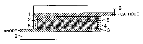
Fig. 1 is a schematic section view of the
main structure of a dye sensitized solar cell
comprising a photoelectric conversion device prepared
by using a sealant according to the present invention.
Reference numeral 1 denotes a conductive support the
inner side of which has conductivity. Reference
numeral 2 denotes a dye-sensitized semiconductor
containing layer. Reference numerals 1 and 2
constitute a semiconductor electrode. Reference
numeral 3 denotes a counter electrode where platinum or
the like is placed on the conductive surface, which is
the inner side, of a conductive support. Reference
numeral 4 denotes a charge transfer layer placed to be
interposed between the conductive supports facing to
each other. Reference numeral 5 denotes a sealant.
Reference numeral 6 denotes a glass substrate.
CA 02613987 2008-01-02
.
48
[0059]
Sealants for photoelectric conversion devices
according to the present invention hardly contaminate
charge transfer layers in processes for producing
photoelectric conversion devices, and excellent in
application workability to substrates, bonding
properties, adhesion strength, available time at room
temperature (pot life), and curability in low
temperatures. *Thus obtained photoelectric conversion
devices according to the present invention do not cause
operation failure due to contaminated charge transfer
layers, and also excellent in adhesion and moisture
resistance reliability. Solar cells prepared by using
such photoelectric conversion devices can be produced
efficiently, and the solar cells are excellent in
durability.
EXAMPLES
[0060]
The present invention is described further in
detail with referring to examples, however, the
invention is not restricted to the examples.
[0061]
Synthesis Example 1: Synthesis of ethylene oxide
addition bisphenol S type epoxy resin (epoxy resin A)
To a flask equipped with a thermometer, a
dropping funnel, a condenser, and a stirrer, 169 parts
of SEO-2 (a tradename for ethylene oxide addition
bisphenol S manufactured by NICCA CHEMICAL CO., LTD.,
CA 02613987 2008-01-02
49
melting point: 183 C, and purity: 99.5%), 370 parts of
epichlorohydrin, 185 parts of dimethyl sulfoxide, and 5
parts of tetramethylammonium chloride were added and
dissolved with stirring; this solution was heated to
50 C. Then 60 parts of flake form sodium hydroxide were
separately added thereto over 100 minutes; subsequently
a reaction was further effected at 50 C for 3 hours.
After the reaction was complete, 400 parts of water was
added thereto and this solution was washed. Excessive
epichlorohydrin and the like were evaporated from an
oil layer at 130 C under a reduced pressure by using a
rotary evaporator. To thus obtained residue, 450 parts
of methyl isobutyl ketone was added and dissolved, and
this solution was heated to 70 C. To this solution, 10
parts of 30% aqueous solution of sodium hydroxide was
added with stirring and a reaction was effected for an
hour. Then this solution was washed with water three
times, and methyl isobutyl ketone was evaporated at
180 C under a reduced pressure by using a rotary
evaporator to obtain 212 parts of liquid epoxy resin A
represented by the following formula (1). The epoxy
equivalent of thus obtained epoxy resin was 238 g/eq,
and the viscosity of the resin at 25 C was 113400 mPa=s.
[0062)
[Formula 3]
O
G- 0-CH2-CH2-0 IS O-CH2-CH2-0-G ( 2~
O
CA 02613987 2008-01-02
s. ,
[0063]
In the formula (1), G represents a glycidyl
group.
[00641
5 Synthesis Example 2: Synthesis of ethylene oxide
addition bisphenol fluorene epoxy resin (epoxy resin B)
In a flask equipped with a thermometer, a
dropping funnel, a condenser, and a stirrer, under
nitrogen gas purge, 220 parts of BPEF (a tradename for
10 bisphenoxyethanol fluorene manufactured by OSAKA GAS
CO., LTD., white solid, and melting point: 124 to 126)
were dissolved in 370 parts of epichlorohydrin, and 5
parts of tetramethylammonium chloride was added
thereto. This solution was heated to 45 C, and 60 parts
15 of flake form sodium hydroxide were separately added
thereto over 100 minutes; subsequently a reaction was
further effected at 45 C for 3 hours. After the
reaction was complete, the solution was washed with
water twice to remove generated salts. After that,
20 excessive epichlorohydrin and the like were evaporated
with heating to 130 C under a reduced pressure by using
a rotary evaporator. To thus obtained residue, 552
parts of methyl isobutyl ketone were added and
dissolved. This methyl ethyl ketone solution was
25 heated to 70 C. To this solution, 10 parts of 30%
aqueous solution by weight of sodium hydroxide were
added, and a reaction was effected for an hour. Then
this solution was washed with water until the pH of a
CA 02613987 2008-01-02
~ -
51
cleaning solution became neutral. Subsequently, a
water layer was separated and removed. Methyl ethyl
ketone was evaporated with heating under a reduced
pressure from an oil layer by using a rotary evaporator
to obtain epoxy resin B represented by the following
formula (2). Thus obtained epoxy resin was semisolid
and the epoxy equivalent of the resin was 294 g/eq.
[0065]
[Formula 4]
Cr- o- CHy-CH2- o 0 - CH2-CIi2- O-G
(2)
[0066]
In the formula (2), G represents a glycidyl
group.
[0067]
Example 1
Bisphenol F epoxy acrylate was obtained by
reaction of RE-404P (a tradename for bisphenol F type
epoxy resin manufactured by Nippon Kayaku Co., Ltd.,
epoxy equivalent: 160 g/eq, and hydrolyzable chlorine
amount: 30 ppm) with 100% equivalent of acrylic acid
based on an epoxy group; purification by a separating
treatment with ion exchanged water/toluene; and
subsequent evaporation of toluene. A resin solution
was obtained by heating at 90 C and dissolving 80 parts
CA 02613987 2008-01-02
52
by weight of thus obtained bisphenol F epoxy acrylate,
20 parts by weight.of epoxy resin A in Synthesis
Example 1, as radical formation photo polymerization
initiators, 1.8 parts by weight of ADEKA OPTOMER-N-1414
(a tradename for 3,6-bis(2-methyl-2-
morphorinopropionyl)-9-n-octylcarbazole manufactured by
Asahi Denka Co., Ltd.), and 1.2 parts by weight of KBM-
603 (a tradename for an aminosilane coupling agent N-
R(aminoethyl)y-aminopropyltrimethoxysilane manufactured
by Shin-Etsu Silicones). To this resin solution cooled
to room temperature, 4.1 parts by weight of IDH-S (a
tradename for isophthalic acid dihydrazide manufactured
by OTSUKA Chemical Co., Ltd., melting point: 224 C,
active hydrogen equivalent: 48.5 g/eq, average particle
diameter: 1.7 m, and maximum particle diameter: 7 m)
obtained by pulverizing jet milled grade IDH-S by using
a jet mill, 30 parts by weight of CRYSTALITE 1FF (a
tradename for molten crushed silica manufactured by
TATSUMORI LTD., and average particle diameter: 1.0 m),
and 1 part by weight of IXE-100 (a tradename for a
zirconium phosphate based ion catcher manufactured by
TOAGOSEI CO., LTD.) were added, and this solution was
kneaded by using a triple roll mill to obtain a sealant
(1) for a photoelectric conversion device according to
the present invention. The viscosity of the sealant at
25 C was 300 Pa=s, which was measured by using an R type
viscometer RU manufactured by TOKI SANGYO CO., LTD.).
[0068]
CA 02613987 2008-01-02
53
Example 2
Bisphenol F epoxy acrylate was obtained by
reaction of the RE-404P with 100% equivalent of acrylic
acid based on an epoxy group; purification by a
separating treatment with ion exchanged water/toluene;
and subsequent evaporation of toluene. A resin
solution was obtained by heating at 90 C and dissolving
80 parts by weight of thus obtained bisphenol F epoxy
acrylate, 20 parts by weight of epoxy resin B in
Synthesis Example 2, as radical formation photo
polymerization initiators, 1.8 parts by weight of the
ADEKA OPTOMER-N-1414, and 1.2 parts by weight of the
KBM-603. To this resin solution cooled to room
temperature, 3.3 parts by weight of the IDH-S
pulverized by using a jet mill, 30 parts by weight of
the CRYSTALITE 1FF, and 1 part by weight of the IXE-100
were added, and this solution was kneaded by using a
triple roll mill to obtain a sealant (2) for a
photoelectric conversion device according to the
present invention. The viscosity of the sealant at 25 C
was 400 Pa=s, which was measured by using the R type
viscometer.
[0069]
Evaluation test 1
Next, each of the sealants obtained in
Examples 1 and 2 was evaluated by determining adhesion
strength, pot life, glass transition temperature, and
the amount of the sealant component leaching to a
CA 02613987 2008-01-02
54
charge transfer layer. The results are shown in Table
1.
[0070]
[Table 1]
Table 1
Example 1 Example 2
Adhesion strength (MPa) 75 75
Pot life (viscosity increase %) 20 20
Glass transition temperature ( C) of 87 87
cured compound
Test of contamination of charge
transfer layer
Total of leaching amount (ppm) 500 650
Epoxy resin A 50 -
Epoxy resin B - 200
Bisphenol F type epoxy diacrylate 450 450
Isophthalic acid dihydrazide (IDH) ND ND
In Table 1, ND represents levels below the limits of
detection. Example 1 does not contain epoxy resin B,
and - is indicated in the corresponding part. Example
2 does not contain epoxy resin A, and - is indicated in
the corresponding part.
[0071]
As is evident from Table 1, the sealants
according to the present invention obtained in Examples
1 and 2 have excellent properties such as adhesion
strength, pot life, glass transition temperature, and
leaching amount. That is, it has been established that
CA 02613987 2008-01-02
" , .
the sealants according to the present invention exhibit
considerably reduced leaching amount to charge transfer
layers while the properties as sealants are maintained.
The tests were conducted by the following methods,
5 respectively.
[0072]
Adhesion strength
To 100 g of each of the sealants, 1 g of 5 m
glass fiber was added as a spacer and mixed with
10 stirring. This sealant was applied to a 50 mm x 50 mm
glass substrate. Onto the sealant, 1.5 mm x 1.5 mm
glass piece was placed. Ultraviolet rays were
irradiated at 3000 mJ/cm2 to the compound by using an
ultraviolet irradiation apparatus, and the compound was
15 cured in an oven at 120 C for an hour. The shear
bonding strength of the glass piece was determined.
[0073]
Pot life
Each of the sealants was left at 30 C, and
20 then viscosity increase rate (%) of the sealant was
determined after a lapse of 48 hours based on the
initial viscosity.
[0074]
Glass transition temperature
25 Each of the sealants was interposed between
polyethylene terephthalate (PET) films to obtain a thin
film of the compound with a thickness of 60 m.
Ultraviolet rays were irradiated at 3000 mJ/cm2 to the
CA 02613987 2008-01-02
56
thin film by using an ultraviolet irradiation
apparatus, and the film was cured in an oven at 120 C
for an hour. After the curing was complete, PET films
were stripped from the thin film to obtain a sample.
TMA test was conducted by using an apparatus
manufactured by ULVAC-RIKO, Inc., and then glass
transition temperature was determined in tension mode.
[0075]
Test of contamination of charge transfer layer
The components of the sealants that leached
to a charge transfer layer due to the contact between
the layer and each of the uncured sealants were
determined by gas chromatography. 0.1 g of the sealant
was placed in a sample vessel, and 1 ml of the
following charge transfer layer (E) was added thereto.
Then with simulating curing conditions of the sealant,
ultraviolet rays were irradiated at 3000 mJ/cm2 to the
sealant by using an ultraviolet irradiation apparatus,
and the compound was subjected to a curing contact
treatment in an oven at 120 C for an hour. After that,
the compound was left at room temperature for an hour,
and then the charge transfer layer after the contact
treatment was transferred to an empty sample vessel.
The components of the sealant that leached to this
charge transfer layer (E) were determined by gas
chromatography with using pentadecane as an internal
standard substance.
[00761
CA 02613987 2008-01-02
57
Composition of charge transfer layer (E): 0.5
M of DMPII (1,2-dimethyl-3-propylimidazolium iodide),
0.05 M of 12 (iodine), and 1.0 M of TBP (t-
butylpyridine) were dissolved in EMI (1-ethyl-3-
methylimidazolium)-TFSI
(bistrifluoromethanesulfonylimide).
[0077]
Example 3
As shown in the example of a photoelectric
conversion device (Fig. 1), a semiconductor electrode 1
was prepared by applying paste of Ti02 particles (P25
manufactured by Degussa Co., Ltd.) as a semiconductor
containing layer to the conductive surface of a FTO
conductive glass support as a conductive support;
firing the substrate at 450 C for 30 minutes; and
immersing the substrate into 3 x 10⁻⁴ M solution of a
dye represented by a formula (3) in ethanol for 24
hours. After that, a counter electrode was prepared by
depositing Pt at a thickness of 200 angstroms also on
the conductive surface of a FTO conductive glass
support.
CA 02613987 2008-01-02
58
[0078]
[Formula 5]
COONBu2
~
HOOC H O O C
N
K~6 htsC
Ru,,,,'
N Nse
~ N
H
~
~
coOrrBU2
[0079]
Then the sealant (1) 5 obtained in Example 1
was applied on the periphery of the counter electrode 3
with remaining a hole for injecting a charge transfer
layer 4 by using a dispenser, and the semiconductor
electrode 1 was overlaid on the counter electrode 3.
After the overlaying, a gap was formed by pressing, and
UV rays were irradiated at 3000 mJ to provisionally
bond the electrodes. Then the electrodes were heated
in an oven at 120 C for an hour to cure the sealant to
bond the electrodes.
[0080]
CA 02613987 2008-01-02
- ~ S
4 59
Next, an iodine-based charge transfer layer
(b) (iodine/lithium iodide/methylhexylimidazolium
iodide manufactured by SHIKOKU CHEMICALS CORPORATION/t-
butylpyridine were dissolved in 3-methoxypropionitrile
so that the composition of thereof became 0.1 M/0.1
M/0.6 M/1 M) was filled in the cell from the hole for
injecting a charge transfer layer of the bonded
electrodes, and the injection hole was sealed with an
epoxy resin, thereby providing a photoelectric
conversion device (cell 1) according to the present
invention.
[0081]
Example 4
A photoelectric conversion device (cell 2)
according to the present invention was obtained as with
Example 3 except that the sealant (2) for a
photoelectric conversion device in Example 2 was used,
and a semiconductor containing layer prepared by
hydrolyzing titanium alkoxide by sol-gel method was
used according to Non-Patent Document 1.
[0082]
Example 5
A photoelectric conversion device (cell 3)
according to the present invention was obtained in
Example 3 where a weir was formed on the periphery of a
conductive support having a semiconductor containing
layer supporting a dye on the support as with Example 1
by using the sealant (1) prepared in Example 1, and a
CA 02613987 2008-01-02
charge transfer layer (a) was dropped in the weir in an
amount so that a 30 gap would be formed; a counter
electrode was overlaid on the support under a reduced
pressure; then a gap was formed by pressing, and UV
5 rays were irradiated at 3000 mJ to provisionally bond
the support and the electrode; and then they were
heated in an oven at 120 C for an hour to cure the
sealant.
[0083]
10 Example 6
A photoelectric conversion device (cell 4)
according to the present invention was obtained as with
Example 3 except that the dye represented by the
formula (3) was replaced with a dye represented by the
15 following formula (4).
[0084]
[Formula 6]
NI~
CN ~ ~ S ~
HooC \ S
~ r (4)
[0085]
Example 7
A photoelectric conversion device (cell 5)
20 according to the present invention was obtained as with
CA 02613987 2008-01-02
61
Example 3 except that the dye represented by the
formula (3) was replaced with a dye represented by the
following formula (5).
[0086]
[Formula 7]
C2H5.N.C2Hg
'
HOOC ~ ~
CN NC2H5 (5)
62H5
[0087]
Example 8
A photoelectric conversion device (cell 6)
according to the present invention was obtained as with
Example 3 except that the dye represented by the
formula (3) was replaced with a dye represented by the
following formula (6).
[0088]
[Formula 8]
- CH3
HOOC H
~ 3
i
N,N O
' i (6)
~
CA 02613987 2008-01-02
62
[0089]
Example 9
A photoelectric conversion device (cell 7)
according to the present invention was obtained as with
Example 3 except that the dye represented by the
formula (3) was replaced with a dye represented by the
following formula (7).
[0090]
[Formula 9)
HOOC CNONO
(7)
[0091]
Comparative Example
A cell of Comparative Example was obtained as
with Example 3 except that commercial HIMILAN
(manufactured by DU PONT-MITSUI POLYCHEMICALS CO.,
LTD.) was used as the sealant.
[0092]
Evaluation test 2
Photoelectric conversion efficiency measurement
Solar cells according to the present
invention were obtained by connecting lead wires to the
both electrodes of each of the obtained photoelectric
conversion devices and placing a voltmeter and an
CA 02613987 2008-01-02
. ~
. ~ ~
63
ammeter. The photoelectric conversion efficiency of
each of the solar cells was measured. The measurement
size of each photoelectric conversion device was 0.5 x
0.5 cm2. As for a light source, a 1 kW xenon lamp
(manufactured by WACOM) was used through an AM 1.5
filter to be at 100 mW/cm2. Short circuit current, open
circuit voltage, and photoelectric conversion
efficiency were measured by using a solar simulator
(WXS-155S-10 manufactured by WACOM).
[0093]
[Table 2]
Table 2
Short circuit Open circuit Photoelectric
current voltage conversion
(mA/cm2) (V) efficiency
M
Cell 1 14.6 0.72 6.5
Cell 2 13.5 0.68 5.9
Cell 3 14.4 0.70 6.4
Cell 4 14.6 0.70 5.8
Cell 5 15.1 0.64 6.1
Cell 6 12.1 0.59 4.8
Cell 7 10.6 0.73 5.2
[0094]
Evaluation test 3
Durability test
The solar cells (cells 1 to 6) used in the
Evaluation test 2 were tested as to durability. Cells
CA 02613987 2008-01-02
64
1 to 6 were in operation for a time period of 180 days
at a constant temperature (25 C). Photoelectric
conversion efficiency (%) of each cell was determined
at the initial stage, after a lapse of 30 to 180 days.
The results are shown in Table 3.
As is evident from Table 3, the conversion
efficiency of each cell did not decrease considerably
at any measurement time, and all the cells exhibited
excellent durability. The cells using an organic dye
represented by (4), (5), (6), or (7) as a sensitizing
agent instead of the metal complex dye (3) also
exhibited good durability. In contrast, as to the
Comparative Example cell using the commercial sealant,
its conversion efficiency was almost halved after a
lapse of 30 days, and decreased to about one sixth of
the initial efficiency after a lapse of 180 days.
[0095]
[Table 3]
Table 3
Initial After a After a After a After a
value lapse of lapse of lapse of lapse of
30 days 60 days 120 days 180 days
Cell 1 6.5 6.3 6.2 6.6 6.4
Cell 2 5.9 5.8 5.5 5.7 5.8
Cell 3 6.4 6.4 6.3 6.5 6.3
Cell 4 5.8 5.9 5.8 6.0 6.1
Cell 5 6.1 6.1 6.1 5.9 5.8
Cell 6 4.8 4.8 4.7 4.6 4.6
Cell 7 5.2 5.3 5.3 5.3 5.3
Comparative 6.4 3.8 1.9 1.9 1.0
Example
CA 02613987 2008-01-02
BRIEF DESCRIPTION OF THE DRAWINGS
[0096]
Fig. 1 is a schematic section view of the
main structure of a photoelectric conversion device
5 according to the present invention.
DESCRIPTION OF SYMBOLS
[0097]
1 denotes a conductive support
2' semiconductor containing layer (1 and 2 constitute
an anode)
3 counter electrode (a cathode)
4 charge transfer layer
5 sealant
6 denotes a glass substrate