Note: Descriptions are shown in the official language in which they were submitted.
CA 02614064 2008-01-02
46920W0
Activatable optical layer
The invention relates to a multilayer body having an
optically active layer system.
Optically active layer systems are used, for example,
for decorative or informative purposes, or in order to
provide security documents with optical security
features which on the one hand make it harder to forge
them using modern color copiers and other reproduction
systems, and on the other hand can easily and clearly
be identified by lay persons.
For this purpose, it is known for security threads to
be incorporated as security elements in valuable
documents, with the arrangement being designed such
that the thread is exposed in places on the surface, so
that the optical security features which are
incorporated in the thread, for example holograms or
partial demetalizations, can be checked by the viewer.
Furthermore, EP 1 134 694 Al discloses an electronic
circuit composed of organic semiconductor material
being printed on a sheet or a strip of paper, and being
connected via a conductor track to a metal strip of a
treasury bill. The electronic circuit is in this case
not based on electronic components formed from
conventional semiconductor materials but on organic
field-effect transistors using polymer semiconductor
technology. The metal strip is in this case used as an
antenna via which it is possible to communicate between
the semiconductor circuit and an appropriate evaluation
circuit. The electronic circuit can therefore be used
to identify forgeries while also allowing the document
to be located.
CA 02614064 2008-01-02
- 2 -
The invention is now based on the object of specifying
a multilayer body having a better visual appearance.
The object of the invention is achieved by a multilayer
body having an optically active first layer system,
with the first layer system being an optically variable
device (OVD) and in which case the optical effect of
the first layer system can be influenced by an
electrically controllable second layer system.
A multilayer body such as this can be designed to be
thin and flexible, thus resulting in particular
advantages for its use and its production. For example,
the multilayer body may be produced at low cost as a
film body using a roll-to-roll process, and is
therefore suitable for mass production.
The multilayer body according to the invention can be
used not only as a novel security element for valuable
documents, security documents and for goods protection,
but also for decorative purposes or product
advertising. Furthermore, the multilayer body can be
used in displays, in RFID tags and as a status
indication in electrical appliances.
Despite the fact that the multilayer body may be thin,
it may be in the form of a large-area film body, for
example applied to packages, windows or building
surfaces.
Further advantageous refinements are specified in the
dependent claims.
The second layer system is advantageously arranged
above the first layer system.
In addition, the optical characteristic of the second
layer system, in particular its optical density and/or
CA 02614064 2008-01-02
- 3 -
its light scattering and/or its color, may be
controllable.
In one advantageous refinement, the second layer system
has an upper and a lower electrode layer, between which
one or more layers is or are arranged. The layers are
preferably layers whose optical characteristics can be
varied by application of a voltage between the
electrode layers.
The upper electrode layer and/or the lower electrode
layer may be composed of polyethylene dioxythiopene
(PBDOT)/PSS or PANI.
It is also possible to provide for the upper electrode
layer and/or the lower electrode layer to be an ITO
(indium tin oxide) layer. Layers such as these are
transparent, conductive layers.
The upper electrode may also be composed of a very thin
translucent metal layer. The metal layer may have a
thickness of 0.5 to 30 nanometers, typically a
thickness of 5 nanometers and may be composed of gold,
silver, chromium, copper or aluminum.
In a further refinement, the second layer system has a
layer which is arranged between the upper and the lower
electrode layer and has a multiplicity of liquid-
crystal bubbles with a diameter of 0.1 um to 40 um,
which are bonded in a polymer matrix. By way of
example, the polymer matrix may be composed of monomers
with a layer thickness of 5 um to 40 um, polymerized by
way of example by UV radiation. By way of example, this
may be the product PN 393 from the Nematel Company. The
liquid-crystal bubbles have liquid crystals aligned
randomly, in an unorganized form. They therefore
scatter incident light so that layers arranged under
the layer cannot be perceived or cannot be imaged
CA 02614064 2008-01-02
- 4 -
sharply. The liquid crystals are aligned in an
electrical field which is formed between the upper and
the lower electrode layer when the electrode layers are
connected to the poles of an electrical voltage source.
The voltage source may be either a DC voltage source or
an AC voltage source. It is also possible to use
electrochemical voltage sources, electrical tuned
circuits, which are located in an electromagnetic field
and whose signal is processed using an electronic
circuit to an appropriate signal frequency, for
example 100 Hz, or to use solar cells as the voltage
source for the multilayer body according to the
invention.
In a further advantageous refinement, the second layer
system has a liquid-crystal-layer, which is arranged
between the upper electrode layer and the lower
electrode layer and at least one polarizer layer. For
example, two polarizer layers can be provided, with
their polarization planes crossed over at 90 . It is
also possible for the liquid-crystal-layer to have
cholesteric liquid crystals. The liquid crystals rotate
the polarization direction of the light through 90 .
This results in the polarized light being able to pass
through the lower polarization layer. The second layer
system therefore appears transparent, and provides a
free view of the first layer system. When an electrical
field is formed between the two electrode layers, the
second layer system appears dark and blocks the view of
the first layer system arranged underneath it.
In addition, it is possible to provide for the second
layer system to have an electrolyte layer which is
arranged between the upper and the lower electrode
layer, and for the upper electrode layer to be an
electrochromic layer, for example composed of an
electrically conductive organic material such as
CA 02614064 2008-01-02
- 5 -
PEDOT/PSS, or polyaniline (PANI). A redox reaction,
which can be controlled by the current direction in the
electrolyte layer, makes it possible to change the
color of an electrochromic layer composed of PEDOT/PSS
from pale blue to dark blue. If the electrochromic
layer is composed of PANI, the color can be changed
from greeny blue to bluey. The electrolyte layer may
also contain metal ions, with the current direction in
the electrolyte layer determining whether metal ions
are transported from the electrolyte layer into the
electrochromic electrode layer, or are moved away from
it. If, for example, the metal ions are tungsten ions,
the electrochromic electrode layer can be varied from
dark blue to colorless.
Other electrochromic systems exist, for example those
which react to a change in pH value. These can likewise
be used.
If the first layer system has an upper electrically
conductive layer, for example a metallic reflective
layer, it is possible for the electrically conductive
layer to form the lower electrode layer of the second
layer system.
In a further advantageous refinement, the second layer
system has a thermochromic layer and an electrical
resistance layer.
It is also possible for at least one layer of the first
layer system to form the electrical resistance layer of
the second layer system.
The second layer system may be designed to have areas
which reproduce image and/or alphanumeric information.
The areas may, for example, be in the form of letters
which form an inscription which can be seen by
electrical actuation of the second layer system. It may
CA 02614064 2008-01-02
- 6 -
also be a barcode which can be seen only when the
multilayer body is placed in an electrical field in a
reader. A feature such as this cannot be forged by
conventional reproduction processes. For example, in an
application such as this, it is possible for the second
layer system to have no electrode layers. In
consequence, the second layer system can advantageously
not be perceived during normal use of the object to
which the multilayer body according to the invention
has been applied.
It is also possible for the optical effect of the
second layer system to be reversibly controllable.
In a further advantageous refinement, the optical
change in the second layer system caused by an
electrical voltage remains after the electrical voltage
is disconnected. For this purpose, the liquid crystals
may be ferroelectric liquid crystals. Ferroelectric
liquid crystals allow the effect of the electrical
field to be stored for a relatively long time, for
example over weeks, and they can be reset by an
electrical pulse. By way of example, this makes it
possible to use a multilayer body with ferroelectric
liquid crystals as a data memory for a due date. The
due date may be visible once a notice period has
elapsed, because the ferroelectric liquid crystals
return to their initial position, and the second
structure layer is transparent again. It is
advantageously possible for a multilayer body such as
this not to have any electrodes, so that the electrical
field which is required to align the ferroelectric
liquid crystals can be formed only in apparatuses
intended for this purpose.
In this case the expression an electrically
controllable layer system means any layer system in
which at least one parameter of its optical effect is
CA 02614064 2008-01-02
- 7 -
changed by application of an electrical voltage. This
is a change in the material characteristic which is
governed by an electrical variable.
The invention provides for the first layer system to
have a replication layer and an optical isolation layer
or a reflective layer and for a diffractive relief
structure to be formed in the replication layer which,
in particular, forms a diffraction grating and/or a
hologram or Kinegram or Trustseal or comparable
system.
Furthermore, the first layer system may be a thin-film
layer system in order to produce color-shift effects,
which are dependent on the viewing angle, by means of
interference.
Layers which produce color changes have a
thickness d = A/4 or d = A/2, where A is the wavelength
of the incident light.
It is also possible to form the thin-film layer system
from a sequence of high-diffractive-index and
low-diffractive-index layers. Layers such as these are
also referred to as HRI (high refractive index) layers
and LRI (low refractive index) layers, respectively.
The greater the number of layers that are chosen, the
more sharply the wavelength of the color change effect
can be set. In this case, it is particularly
advantageous for a thin-film layer system such as this
to be formed from two to ten layers (even-number
variants) or three to nine layers (odd-number
variants).
The first layer system may also be a layer system which
has a cholesteric liquid-crystal-layer and an
absorption layer. A layer system such as this has a
color shift effect which is dependent on the viewing
CA 02614064 2008-01-02
- 8 -
angle, in a similar manner to that of a thin-film layer
system.
Systems are also feasible which require only one
electrode plane. By way of example, this may be a
heating element for a thermochromic layer or a layer
system as described above with cholesteric liquid
crystals which can be actuated in that plane. The layer
arranged under the liquid crystals may have projections
at a distance from one another and with a width of
about 20 lam and a height of 20 um to 100 pm, arranged
at a distance of less than 100 um. An OVD as described
above may be formed between the projections and
optically appears as an entity, because of the small
dimensions of the projections. The electrodes which are
formed on the projections form areas in the form of
strips, which are connected alternately and switchably
to the poles of a voltage source. The electrical field
formed between the areas therefore runs within the
liquid-crystal layer, and not at right angles to the
liquid-crystal layer.
It is also possible for the projections to be arranged
like a chequerboard and/or for the first and/or the
second layer system to be appropriately structured, and
for the connecting lines to be in the form of a matrix
so that each electrode area can be actuated in rows and
columns.
It is also possible to actuate the liquid crystals
located between an upper electrode layer and a lower
electrode layer (which is structured like a
chequerboard) at specific points. It is therefore
possible for liquid crystals which are arranged over
actuated areas of the lower electrode layer to be
aligned in the electrical field, and for liquid
crystals which are arranged over unactuated areas of
the lower electrode layer to retain the unorganized
CA 02614064 2008-01-02
- 9 -
alignment. The actuated or the unactuated areas may in
this way form a pattern, for example representing an
image, a logo or one or more alphanumeric characters.
The areas which are electrically isolated from one
another may be actuated alternately, so that the
sub-areas successively change their optical appearance.
In a further refinement, the multilayer body has drive
electronics, which are preferably organic drive
electronics.
It is also possible for the multilayer body to have one
or more sensors and/or RFID circuits and/or displays
and/or switches and/or voltage sources.
The two embodiments mentioned above provide a rough
outline of the field of application of the multilayer
body according to the invention, although this does not
restrict further applications.
It is also possible for the multilayer body to be
designed to be flexible and/or to have a flexible,
transparent carrier film. A flexible multilayer body
can advantageously also be applied to curved surfaces.
It has particularly good resistance to bending loads,
such as those which can occur on thin carrier
substrates, for example packages, treasury bills or
documents.
In particular, flexible multilayer bodies can be
produced at low cost as mass-produced items on
installations which are intended for a roll-to-roll
process. In this case, additional assemblies, such as
RFID tags, solar cells, batteries, storage devices,
integrated circuits, film switches and sensors can
easily be integrated in the multilayer body.
CA 02614064 2008-01-02
- 10 -
The invention will be explained in the following text
using, by way of example, a number of exemplary
embodiments and with the assistance of the attached
drawings, in which:
Figures la and lb show a first exemplary embodiment of
a multilayer body according to the invention in the
form of a schematic section illustration;
Figures 2a and 2b show a second exemplary embodiment
of a multilayer body according to the invention in the
form of a schematic section illustration;
Figures 3a and 3b show a third exemplary embodiment of
a multilayer body according to the invention in the
form of a schematic section illustration;
Figures 4a and 4b show a fourth exemplary embodiment
of a multilayer body according to the invention in the
form of a schematic section illustration;
Figures 5a and 5b show a fifth exemplary embodiment of
a multilayer body according to the invention in the
form of a schematic section illustration;
Figures 6a to 7b show one application example of a
multilayer body according to the invention.
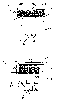
Figures la and lb show a schematic section illustration
of a multilayer body 1 with an optically variable layer
system 10 and a controllable layer system 20.
The layer system 10 is an optically variable
device (OVD) with a structure layer 12 in which a
diffraction grating 12b is formed. The structure layer
12 may, for example, be formed from a thermoplastic
replication varnish with a layer thickness of a few 1.1m,
in which the diffraction grating 12b has been impressed
ak 02614064 2008-01-02
- 11 -
with the aid of a heated replication roller. The
structure layer 12 is covered with a metallic
reflective layer 14 which, for example, is composed of
aluminum, silver, chromium, copper or gold.
The controllable layer system 20 has a carrier layer 22
which is arranged on the metallic layer 14. The carrier
layer 22 is a polymer matrix in which a multiplicity of
liquid-crystal bubbles 22f are embedded. The liquid-
crystal bubbles have a diameter of 0.1 pm to 15 pm. The
polymer matrix is composed of PN393, which can be
applied with a layer thickness from 5 pm to 40 pm. The
layer thickness is preferably 10 pm.
A transparent protective layer 26 is arranged on the
carrier layer 22 and has an electrode layer 24 on its
lower face. In this exemplary embodiment, the layers 26
and 24 are transparent, conductively coated Orgakonm
film from Agfa, with the electrode layer 24 being a
transparent conductive polymer. This is PEDOT/PSS,
which may have a layer thickness from 50 nanometers to
500 nanometers. The layer thickness is preferably 200
nanometers. The electrode layer 24 may also be a
transparent metallic layer.
An electrical field, in which the liquid crystals
contained in the liquid-crystal bubbles 22f can be
aligned, can be formed by application of an electrical
voltage between the electrode layer 24 and the metallic
reflective layer 14. In Figures la and lb, the liquid
crystals are symbolized by short lines. In this
exemplary embodiment, the metallic reflective layer 14
is therefore at the same time an electrode layer for
the electrically controllable layer system 20. It is
therefore a multiple-function layer.
The electrical voltage for controlling the layer system
20 is produced by an electrical voltage source 30 which
CA 02614064 2008-01-02
- 12 -
is electrically conductively connected to the layers 14
and 24 by means of connecting lines 34 and 34' and a
switch 32. The connecting lines 34, 34', which are
illustrated symbolically in Figures la and lb, may be
conductor tracks which are formed by continuing the
electrically conductive layers 14 and 24. However,
there may also be metallic conductor tracks which make
electrical contact with the layers 14 and 24 and, for
example, are vapor-deposited.
Figure la shows the multilayer body 1 with the switch
32 open. The liquid crystals arranged in the liquid-
crystal bubbles 22f assume an unorganized random
position, so that light striking the multilayer body 1
is reflected diffusely, as a result of which the first
layer system 10 cannot be seen, or can be seen only
insignificantly, and cannot produce an optical effect.
Figure lb now shows the multilayer body 1 with the
switch 32 closed. An electrical field is now formed
between the layers 14 and 24, with its field lines
aligned at right angles to the surface of the layers 14
and 24, so that the liquid crystals arranged in the
liquid-crystal bubbles 22f now assume an organized
position, aligned parallel to the electrical field
lines. Because of their small diameter of a few
nanometers, light which is incident on the multilayer
body 1 can now virtually entirely strike the surface of
the structure layer 12 covered with the reflective
layer 14, so that the first layer system 10 can develop
its optical effect, as an OVD.
The polarity of the electrical voltage source 30 is
irrelevant to the principle of operation of the
alignment of the liquid crystals with the electrical
field lines, on which the exemplary embodiment
illustrated in Figures la and lb is based. The
electrical voltage source 30 may therefore be either
CA 02614064 2008-01-02
- 13 -
a DC voltage source or an AC voltage source. The
voltage emitted from the voltage source 30 is
essentially of importance to the formation of the
electrical field that is suitable for alignment of the
liquid crystals. A voltage of approximately 20 V is
provided in the exemplary embodiment illustrated in
Figures la and lb.
In the exemplary embodiment illustrated in Figures la
and lb, the voltage source 30 can be switched on and
off by means of the switch 32. However, it is also
possible to dispense with the switch 32 and for the
voltage source 30 to be in the form of a tuned circuit
in which an external electromagnetic field induces
an AC voltage which, if required, is also converted to
a DC voltage by means of a rectifier. This DC voltage
can be converted back to an AC voltage in the
particularly advantageous frequency range around 100 Hz
by means of suitable electronics, for example a ring
oscillator. A capacitor may also be provided which,
when driven with DC voltage, also produces this DC
voltage for a certain time after the electromagnetic
field has been switched off. If, for example, the
multilayer body forms a so-called RFID tag, that is to
say a circuit arrangement for radio-frequency-assisted
identification of objects, the elements mentioned above
may be components of an RFID tag such as this. The RFID
tag may advantageously be an organic film circuit.
Figures 2a and 2b now show a multilayer body l' which
does not have a second electrode layer (see the
electrode layer 24 in Figures la and lb). In fact, the
structure layer 12 now has a relief structure which has
projections with a width of about 20 lam and a height
of 20 um to 100 um, which are arranged at a distance of
less than 100 um. The diffraction gratings 12b are
formed in the structure layer between the projections,
and are also illustrated in Figures la and lb. The
CA 02614064 2008-01-02
- 14 -
metallic reflective layer 14 now forms areas which are
arranged on the projections, are in the form of strips
and are alternately connected to the connecting lines
34 and 34', so that the areas of the reflective layer
14 which are in the form of strips are alternately
connected to the positive pole or negative pole of the
voltage source 30 when the switch 32 is closed (see
Figure 2b). The electrical field formed between the
areas therefore runs within the carrier layer 22 and
not, as in the case of the first exemplary embodiment
illustrated in Figures la and lb, at right angles to
the carrier layer 22. However, the liquid crystals that
are located in the liquid-crystal bubbles 22f are
aligned analogously to Figure lb in the electrical
field when the switch 32 is closed, as illustrated in
Figure 2b.
It is also possible to arrange the projections like a
chequerboard in the structure layer 12 and for the
connecting lines to be in the form of a matrix so that
each area of the reflective layer 14 can be actuated in
rows and columns. A further exemplary embodiment, which
is not illustrated, can additionally provide an
electrode layer 24, as illustrated in Figures la
and lb, so that, with the aid of the reflective
layer 14 which is structured like a chequerboard, the
liquid crystals which are arranged above actuated areas
of the reflective layer 14 are aligned in the
electrical field, and the liquid crystals which are
arranged above unactuated areas of the reflective
layer 14 retain the unorganized alignment. The actuated
areas or the unactuated areas may in this way form a
pattern, for example representing a logo or one or more
alphanumeric characters.
Figures 3a and 3b now show a multilayer body 2 which
differs from the multilayer body I illustrated in
Figures la and lb only by the formation of the
CA 02614064 2008-01-02
- 15 -
controllable layer system. A controllable layer system
40 has a liquid-crystal-layer 42 in which liquid
crystals 42f are embedded and make it possible to
rotate the polarization plane of polarized light.
The upper face of the liquid-crystal-layer 42 is
covered by an upper polarizer layer 46o, and the lower
face of the liquid-crystal-layer is covered by a lower
polarizer layer 46u. The polarization directions of the
polarizer layers 46o and 46u are crossed over at 90 .
Incident light is therefore polarized before it enters
the liquid-crystal-layer. The liquid crystals now
rotate the polarization plane of the polarized light
through 90 . In consequence, the polarized light can
pass through the lower polarization layer 46u, and is
reflected on the reflective layer 14 of the layer
system 10. The reflected light is now once again
rotated by the liquid crystals 42f which are arranged
in stacks, and emerges from the upper polarizer
layer 46o. The layer system 40 therefore appears to be
transparent, and provides a free view of the layer
system 10, which is in the form of OVD.
The transparent protective layer 26 is arranged on the
upper polarization layer 46o, and has the electrode
layer 24 on its lower face. As already stated above,
the layers 26 and 24 are, for example, composed of a
transparent, conductively coated OrgakonTM film. The
electrode layer 24 is connected to the voltage source
30 via the connecting line 34' and the switch 32. The
other pole of the voltage source 30 is connected to the
metallic layer 14 by the connecting line 34. This
allows an electrical field to be formed between the
layers 14 and 24 by closing the switch 32, thus moving
the liquid crystals 42f to a position such that the
light which has been polarized by the upper
polarization layer 46o can no longer pass through the
lower polarization layer 46u. This state of the
CA 02614064 2008-01-02
- 16 -
multilayer body 2 is illustrated in Figure 2b, in which
it is no longer possible to observe the optical effect
formed by the layer system 10.
It is also possible to provide for the upper
polarization layer 46o and the lower polarization
layer 46u to be arranged with the same polarization
direction, so that the electrically controllable layer
system 20 appears to be opaque when the voltage is
switched off, and appears to be transparent when the
voltage is switched on.
Furthermore, ferroelectric liquid crystals may be
provided for the liquid-crystal-layer 42f.
Ferroelectric liquid crystals have the characteristic
of storing electrical fields so that the switching
state of a liquid-crystal-layer formed by ferroelectric
liquid crystals is also maintained for a relatively
long time after the voltage has been switched off. This
liquid-crystal-layer can be reset by a switching pulse.
Figures 4a and 4b now show a multilayer body 3 in which
an electrically controllable layer system 50 is
arranged on the optically variable layer system 10, is
formed from an electrolyte layer 52 and makes contact
with two electrode layers. As in the exemplary
embodiments described above, the lower electrode layer
is formed by the reflective layer 14 in the layer
system 10. An upper electrode layer 54 is formed from
an electrochromic material, for example from PEDOT/PSS.
The upper electrode layer 54 is covered by the
protective layer 26. The two electrode layers 14 and 54
are connected to the voltage source 30 by means of the
connecting lines 34 and 34', which are connected to a
switch 32u. In the third exemplary embodiment
illustrated in Figures 3a and 3b, the voltage source 30
is a DC voltage source, whose polarity governs the
optical state of the electrochromic electrode layer 54.
CA 02614064 2008-01-02
- 17 -
In this case, an electric current whose current
direction is governed by the position of the switch 32u
flows through the electrolyte layer 52 and which
current, in the illustrated exemplary embodiment,
transports metal ions from the electrolyte layer 52
into the electrochromic electrode layer 54, or removes
them from it. If, for example, these are tungsten ions,
the electrochromic electrode layer 54 may be changed
from dark blue to colorless. As described further
above, other embodiments are possible which are based
on redox reactions, governed by the current direction,
or on the change in the pH value of the electrolyte
layer.
The switch 32u is a two-pole changeover switch, by
means of which the current direction of the electric
current flowing through the electrolyte layer 52 can be
reversed. This allows the electrochromic electrode
layer 54 to be changed from a first, colored, opaque
state to a colorless, transparent state.
Figures 5a and 5b show a multilayer body 4 in which an
electrically controllable layer system 60 is arranged
on the optically variable layer system 10 and has a
thermochromic layer 62. The thermochromic layer 62 in
the illustrated exemplary embodiment is composed of
TCX B-31 from the Coates Screen Company with a layer
thickness of about 20 pm. The layer thickness may be
between 0.5 and 100 pm. the thermochromic layer 62 is
covered by the protective layer 26.
The metallic reflective layer 14 of the layer system 10
is connected to the voltage source 30 by means of the
electrical connecting lines 34, 34' and the switch 32,
and at the same time forms an electrical resistance
layer for heating the thermochromic layer 62. As in the
case of the previous exemplary embodiments, the
reflective layer 14 is therefore a layer which can be
CA 02614064 2008-01-02
- 18 -
functionally associated with both layer systems of the
multilayer body. However, it is also possible to
provide a separate resistance layer, particularly when
the reflective layer 14 cannot be adequately
electrically loaded. In a situation such as this, the
resistance layer is transparent and, for example, is
composed of ITo (indium tin oxide) or some other
conductive material. By way of example, PEDOT/PSS or
PANI may also be used for transparent resistance
layers. The resistance layer may also be arranged under
the structure layer 12 and, in this case, need not be
transparent.
As can be seen in Figure 5a, the thermochromic layer 62
is not transparent when the switch 32 is open. If the
switch 32 is now closed, as illustrated in Figure 5b,
the reflective layer 14 is heated by the start of the
current flow and, in consequence, the thermochromic
layer 62 arranged on the reflective layer 14 is also
heated and in this way becomes transparent. The optical
effect formed by the optically variable layer system 10
can now be seen.
Figures 6a to 7b now show one exemplary embodiment of
the multilayer body according to the invention.
Figure 6a shows a schematic section illustration of a
multilayer body 5 designed in the same way as the
multilayer body 1 illustrated in Figures la and lb. In
this case, some of the layers from Figures la and lb
are in each case combined.
A layer 52 with liquid-crystal bubbles bonded in a
polymer matrix is provided with an upper electrode
layer 54 and is arranged on an OVD layer system 56,
which is illustrated in Figures la and lb and is formed
from a replication layer and a metallic reflective
layer. The reflective layer facing the OVD layer system
CA 02614064 2008-01-02
- 19 -
at the same time forms the lower electrode layer for
the layer 52.
Figures 6b now shows a schematic plan view of the
multilayer body 5, whose electrode layers are connected
to a voltage source 58 by means of connecting lines 581
and a switch 58s. The OVD layer system 56 has an
inscription 56s, which cannot be seen significantly, or
cannot be seen at all, because of the layer 52, which
is opaque when no voltage is applied.
Figures 7a and 7b show the multilayer body 5 whose
electrode layers are now connected to the voltage
source 58, because the switch 58s is closed. The
layer 52 is therefore a clear layer, so that the
inscription 56s, which is arranged on the OVD layer
system 56, can now clearly be read. Furthermore, the
optical effect can now be seen and, for example, may be
a color change which results when the multilayer body 5
is tilted. It is also possible for the inscription 56s
to exhibit an optical effect that is dependent on the
viewing angle, for example apparently changing its
position.
The multilayer body according to the invention may have
further layers, for example an adhesive layer, which is
applied to the rear face of the optically variable
layer system, or layers which form functional elements
such as voltage sources, sensors or electronic
circuits. The layers may preferably be formed from
polymers, in particular also to form electronic
circuits. However, the expression "organic" circuits
should expressly also be understood as covering
circuits and circuit arrangements which also have
inorganic layers as well as organic layers, or only
inorganic layers.
CA 02614064 2008-01-02
- 20 -
The multilayer body according to the invention is also
distinguished in that it can be formed to be thin and
flexible, thus resulting in particular advantages for
its application and its production. For example, the
multilayer body may be produced as a film body using a
roll-to-roll process at low cost, and is therefore
suitable for mass production.
The multilayer body according to the invention may also
have an inflexible carrier material, for example
composed of glass or ceramic, without departing from
the scope of the invention.
Furthermore, the multilayer body according to the
invention may also be designed to irreversibly change
its optical characteristics. For example, it is
possible for the change to be caused by a brief
overvoltage, and for the multilayer body to permanently
signal that an overload has occurred. An effect such as
this may be initiated, for example in the case of
electrochromic layers, by an irreversible chemical
process in the electrolyte layer.