Note: Descriptions are shown in the official language in which they were submitted.
CA 02614427 2007-12-13
214134
METHOD AND APPARATUS FOR RECOGNIZING A CHANGE-OF-STATE IN
COMMUNICATION SIGNALS OF ELECTRONIC CIRCUITS
BACKGROUND OF THE INVENTION
FIELD OF THE INVENTION
The present invention relates in general to electronic circuitries and, more
particularly, to methods and apparatuses for recognizing a valid change-of-
state of
capacitively coupled signals using adaptively active impedance.
DESCRIPTION OF THE RELATED ART
It is common practice in industry to establish communication from a
plurality of input contacts 2 of an electronic circuitry in one device to a
plurality of
output contacts 4 of another by connecting the corresponding contacts from
each via a
cable bundle 6, as illustrated in FIG. 1. One example of such is the
connection of
breaker contact outputs with a protection relay contact inputs in a substation
of a
power grid. When a breaker contact closes, a voltage is applied to the contact
input.
If that voltage is maintained above a preset threshold value for a
predetermined
amount of time (typically known as the debounce timer), the contact input
recognizes
that the applied voltage corresponds to a valid state change and thus the
state of that
input contact is changed from an OFF state to an ON state. The process is
similar for
an input transition from the ON state to the OFF state when the applied
voltage drops
below a second preset threshold for the duration of the debounce timer.
However, the long bundle of cables typically used to connect these devices
is known to introduce large parasitic capacitive coupling between individual
conductors carrying the monitored signals. This is illustrated in FIG. 2,
where a
simplified circuit is illustrated to represent the assembly of FIG. 1. In FIG.
2, the
contact inputs 2 have respective impedance Ra and Rb and switches SWa and SWb
represent the contact outputs 4. In operation, if switch SWa closes, a valid
signal will
1
CA 02614427 2007-12-13
214134
appear continuously on the corresponding contact input Ra. However, a
capacitively
coupled signal will also discharge via a parasitic capacitance (Ci;ne, as
shown in FIG.
2) through the contact input Rb (shown by the dotted line in FIG. 2), even
though the
switch SWb is open.
Two conventional solutions exist for the above-noted problem. The first
includes increasing the debounce timer, and the second includes lowering of
the input
impedance. In order to reject the capacitively coupled pulse, a validation
timer (also
known as a debounce timer) can be used to ignore all pulses under a preset
duration.
The user must configure the debounce timer to ignore pulses with durations
less than
the worst-case capacitively coupled pulse. However, one of the drawbacks in
increasing the duration of the debounce timer is that it delays the
recognition of valid
contact input transitions, which in turn can affect the efficiency of the
protection
scheme. Another approach used to mitigate the effects of capacitively coupled
transients is to reduce the impedance of the contact input. By reducing this
impedance the capacitively coupled signal has a shorter pulse duration that
can then
allow for a smaller debounce timer setting. However, another drawback of this
solution is that the amount of power dissipated by the contact input circuitry
increases
as the impedance decreases, leading to a limitation in the number of contact
inputs
that may be available in the product. Therefore in order to prevent false
input state
changes due to capacitively coupled transients either the number of contact
inputs
must be reduced or the recognition time for an input state change must be
increased.
Conventional solutions to the above-summarized challenge have involved
finding a balance between response time (i.e., the time before the contact
input can
successfully determine if the signal was a transient pulse or a valid input
state change)
and power dissipation (i.e., how many contact inputs can be used in a device
without
destroying the circuitry through heat dissipation). However, this balance
between
power dissipation and contact input response time leads to the current
practical
limitations within the industry for the number of inputs that can be designed
into a
product as well as the practical limitations to the response time of a contact
input to a
valid signal transition.
2
CA 02614427 2007-12-13
214134
Therefore, a need exist to control the impedance of a contact input such
that the current consumed thereby is increased only during the period of time
when
the input is either in the OFF state or in a transition state and reduced
during the
period of time when the contact input is in the ON state, in which power
consumption
is at its peak. Such an approach will not only allow the contact input to
consume
substantially less power during steady state operation than conventional
contact
inputs, but will also allow for a significant improvement in recognition time.
Since
the contact input is only drawing an increased amount of current for a short
duration,
the amount of current drawn can be maximized for recognition time performance.
BRIEF SUMMARY OF THE INVENTION
One or more of the above-summarized needs and/or others known in the
art are addressed by methods for recognizing a valid change of state in a
communication signal received by a first input contact, such methods including
the
steps of maintaining the first contact input in a first state and an impedance
of the first
contact input in a first impedance level; validating that the communication
signal sent
from the first output contact to the first input contact is a valid change of
state for the
first input contact; and changing the first input contact to a second state
and the
impendence of the first input contact input to a second impedance level when
the
voltage communication signal is validated.
One or more of the above-summarized needs and/or others known in the
art are also addressed by input contact circuits that include a signal
converter
electrically coupled to input connections of the input contact circuit; a
switch
electrically coupled to the input connections of the input contact circuit in
parallel
with the signal converter; a current generator electrically coupled in series
to the
switch; an impedance controller electrically coupled to the signal converter
and the
switch; and an input state logic circuit electrically coupled to the signal
converter and
configured to change a state of the input contact from a first state to a
second state.
The above brief description sets forth features of the present invention in
order that the detailed description that follows may be better understood, and
in order
that the present contributions to the art may be better appreciated. There
are, of
3
CA 02614427 2007-12-13
214134
course, other features of the invention that will be described hereinafter and
which
will be for the subject matter of the appended claims.
In this respect, before explaining several preferred embodiments of the
invention in detail, it is understood that the invention is not limited in its
application
to the details of the construction and to the arrangements of the components
set forth
in the following description or illustrated in the drawings. The invention is
capable of
other embodiments and of being practiced and carried out in various ways.
Also, it is
to be understood that the phraseology and terminology employed herein are for
the
purpose of description and should not be regarded as limiting.
As such, those skilled in the art will appreciate that the conception, upon
which disclosure is based, may readily be utilized as a basis for designing
other
structures, methods, and systems for carrying out the several purposes of the
present
invention. It is important, therefore, that the claims be regarded as
including such
equivalent constructions insofar as they do not depart from the spirit and
scope of the
present invention.
Further, the purpose of the foregoing Abstract is to enable the U.S. Patent
and Trademark Office and the public generally, and especially the scientists,
engineers and practitioners in the art who are not familiar with patent or
legal terms or
phraseology, to determine quickly from a cursory inspection the nature and
essence of
the technical disclosure of the application. Accordingly, the Abstract is
neither
intended to define the invention or the application, which only is measured by
the
claims, nor is it intended to be limiting as to the scope of the invention in
any way.
BRIEF DESCRIPTION OF THE DRAWINGS
A more complete appreciation of the invention and many of the attendant
advantages thereof will be readily obtained as the same becomes better
understood by
reference to the following detailed description when considered in connection
with the
accompanying drawings, wherein:
FIG. 1 illustrates a schematic of conventional contact inputs and outputs
connected by a cable bundle;
4
CA 02614427 2007-12-13
214134
FIG. 2 illustrates an electronic circuit representation corresponding to the
schematic of FIG. 1;
FIG. 3 illustrates a generalized flow chart of a method to recognize a
change of state of a contact input in accordance with aspects of the present
technique;
FIG. 4 illustrates another generalized flow chart of a method to recognize a
change of state of a contact input in accordance with aspects of the present
technique;
FIG. 5 illustrates a schematic of a circuit for recognizing a change of state
of a contact input in accordance with aspects of the present technique;
FIG. 6 illustrates a schematic of another circuit for recognizing a change of
state of a contact input in accordance with aspects of the present technique;
and
FIG. 7 illustrates a variation of voltage as a function of time with respect
to
several threshold levels for the circuit of FIG. 6.
DETAILED DESCRIPTION OF THE PREFERRED EMBODIMENTS
Referring now to the drawings, wherein like reference numerals designate
identical or corresponding parts throughout the several views, a generalized
method to
actively control the impedance of a contact input is shown in FIG. 3. As
referred
herein throughout, adaptive active impedance, and its control, corresponds to
adjusting a current draw or resistance of a measuring device during state
transitions in
order to optimize a response of the measuring device to a measured quantity
that can
be optimized by adjusting the impedance dynamically. Examples of measured
quantities, include, but are not limited to, the response time and power
consumption
of an input contact. This allows for an improvement in response time without
sacrificing the number of contact inputs and without increasing the amount of
heat
dissipated in the device containing the contact inputs, as it will be further
explained
below. In the description of exemplary embodiments that will follow, several
examples are given of sample periods, different threshold values, and other
quantities.
As understood by those of ordinary skill in the applicable arts, those
examples are to
be taken as non-limiting, the proper scope of the present invention being
determined
CA 02614427 2007-12-13
214134
only by the broadest interpretation of the appended claims so as to encompass
all
possible modifications and equivalents.
As shown in FIG. 3, the state of a contact input is initially OFF as well as
its impedance is low at 10. The disclosed contact input change-of-state
recognition
process involves measuring the value on the input terminals and comparing that
value
against several thresholds, including, but not being limited to, a bounce
threshold, a
validate threshold, an active impedance, or AZ, threshold, and a low
threshold. Once
the contact input detects a communication signal from a contact output that is
above
the bounce threshold at 20, a process to validate the change of state of the
contact
input is initiated, while maintaining the impedance of the contact input low
at 30. If
the detected communication signal remains above the validate threshold longer
than a
preset duration at 40, indicative of a valid change of state from OFF to ON
and not a
transient due to, for example, a capacitively coupled signal, the state of the
contact
input and its impedance are changed to ON and high at 50, respectively. By
lowering
the impedance at 30 the time to discharge a capacitively coupled transient is
accelerated, resulting in a reduction in the allowable debounce timer and an
improvement in the response time. As further illustrated in FIG. 3, when the
input is
in the ON state, at 50, once the communication signal falls below an active
impedance, or AZ, threshold value, at 60, the impedance is again lowered at 30
in
order to improve the decay constant of the contact input in the presence of
parasitic
input capacitance. The process to validate a new change of state of the
contact input
is initiated when the input voltage falls below the low threshold at 60, where
the input
will change state if all measured values are below the low threshold for the
validation
time. At 70, if the newly detected communication signal remains below the low
threshold longer than the preset duration or debounce timer value, the state
of the
input will change from ON to OFF. If the validation of the input fails and all
values
return to above the validate threshold at 40, for example due to a voltage
sag, the
contact input is switched back to the ON state and its impedance increased at
50. As
such, the control of contact impedance is accomplished such that the current
consumed by a contact input is increased only during the period of time when
the
input is in transition or when the input is in the OFF state, resulting in an
overall
6
CA 02614427 2007-12-13
214134
reduction in power consumed since it is in these two situations that the power
dissipation is minimized. Such an approach will not only allow the contact
input to
consume substantially less power than conventional contact inputs, but it will
also
improve the overall response time and reset time of a contact in the presence
of
parasitic capacitances.
In another embodiment of the invention, the contact input first detects a
state transition of a contact output with a nominal wetting voltage through
the
continuous measurements of voltages present at the contact input terminals and
comparison of those measurements to a threshold value. Once a state transition
is
detected, the contact input initiates a validation process to determine if a
valid state
change of the contact output took place. The detection of the state transition
may
include allowance for a bouncing contact signal. Contact bounce (also known as
chatter) is a common characteristic of mechanical switches and relays. Switch
and
relay contacts are usually made of springy metals that are forced into contact
by an
actuator. When the contacts strike together, their momentum and elasticity act
together to cause bounce. The result is a rapidly pulsed electrical current
instead of a
clean transition from zero to full current. The waveform is then further
modified by
the parasitic inductances and capacitances in the switch and wiring, resulting
in a
series of damped oscillations. This effect is usually unnoticeable in AC mains
circuits,
where the bounce happens too quickly to affect most equipment, but causes
problems
in some analog and logic circuits that are not designed to cope with
oscillating
voltages.
When detecting a bouncing contact signal, two thresholds may be used to
de-bounce the signal, the first threshold being lower than the second. When
the first
threshold is reached (otherwise known as the bounce threshold) the contact
input
enters a bounce period, in which the contact input waits a predetermined time
period,
where the contact output is allowed to freely "bounce" between the ON and OFF
states. Once the wait period is over, the contact input will then begin
validating the
contact input, whereupon the input will change its state to ON if the
validation process
is successful. When the bounce time is set to 0 ms, the input enters the
validation
period in the sample following the sample that reached the bounce threshold.
In the
7
CA 02614427 2007-12-13
214134
application of detecting a valid state transition, after correctly determining
the state of
the contact input signal, a time in which the state transition occurred
(otherwise
known as the time stamp of the contact input event) is determined. Therefore,
by
entering the validation state through the use of a bounce threshold, which is
lower
than the validate threshold, the input becomes more sensitive to contact input
transitions, thus improving time stamp accuracy.
The validation period (or the debounce timer when the bounce timer is set
to zero) measures contact input values and compares them to the validate
threshold.
In one embodiment, a sliding window approach is used, where the contact input
changes state once the contact input has detected valid measurements for an
entire
validation period. The contact will change state to ON if all samples within
the sliding
window are above the validate threshold and will enter the OFF state if all
samples
within the sliding window are below the low threshold.
If during validation, after the first validation period, the contact input
has not validated to either an "ON" or "OFF" state, the contact input will
remain in its
previous state, activate an invalid flag, and continue the validation process.
The input
may fail validation and go invalid if there exists for one validation period
either
measured samples between the high and low threshold or there exists samples
both
above and below the high threshold. If the invalid flag remains high for at
least a
predetermined amount of time (e.g., 1 s), a trouble shooting flag will be set
and an
event will be generated, for system protection, the trouble shooting flag
being reset
after the contact input has not been invalid for a given time period (e.g., at
least 2 s).
In another embodiment, once a change of state of the contact input is
determined, including allowance for the bouncing contact signal, flexible
logic
operands may be used to indicate the state of the contact input. For example,
a
flexible logic operand may be provided for each contact input with
states corresponding to "ON" and "OFF" while a second may be available to
disclose
contact input trouble. For example, the second operand may not go active
unless at
least one of the following conditions occur: (1) the contact input is
considered as
chattering; (2) the contact input has been in the invalid state for a given
amount of
8
CA 02614427 2007-12-13
214134
time (e.g., 1 s); or the contact input has had a self detected hardware
failure within
that given amount of time.
The input contact of the present invention may also provide immunity
against capacitively coupled signals. Capacitively coupled signals exist due
to long
parallel lines typically used in the wiring of contact inputs. These noisy
pulses can last
in excess of 25 ms, leading to false recognition of the contact input state or
a delay in
the recognition of valid contact input state transitions. The decay time of
the
capacitively coupled signal is proportional to the impedance of the contact
input. The
lower the impedance, the faster a capacitively coupled transient will
dissipate
resulting in shorter transient pulse durations. In the instant invention,
dynamic
impedance is used to minimize power dissipation during steady state operation,
while
maximizing noisy signal immunity during state transitions. This is
accomplished as
explained next.
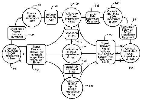
As illustrated in the state diagram shown in FIG. 4, at 80, if the contact
input is OFF and the contact input impedance is low. If a contact output
closure
occurs, an increase in voltage will be seen on the contact input terminals and
the
voltage will increase above the bounce threshold (85) and the contact input
will
transition to the bounce state (90). The bounce state is a wait state used to
optimize
the contact input change-of-state recognition process by taking into account
the
bounce of a contact, which may be disabled (i.e., the change-of-state
recognition
process transitions on the subsequent sample period, e.g., in 250 s, if that
is the
sample period). Once the wait period is over (95), the change-of-state
recognition
process will transition to the validation state, until either the input is
validated or until
a specified amount of time, e.g. I ms, has passed. If the input has not
validated after I
ms (110) the input will shut off the active impedance circuitry and continue
validation
(115). The 1-ms shutdown is due to the fact that the input would dissipate any
transients within 1 ms. If the input successfully validates by measuring all
samples
within the validation period as being above the validate threshold (105), the
input will
transition to the ON state (130). If samples within the validation window were
found
to be both above the validate threshold and below the low threshold or if
samples
9
CA 02614427 2007-12-13
214134
were found to be between both thresholds (120), the input will set the invalid
flag and
continue validation (125). If the input is ON and a measurement on the input
terminals is found to be below the AZ threshold (135) the impedance will again
be
lowered (140). The impedance is lowered in this case in order to increase the
discharge time of a contact input with parasitic capacitance on the input
terminals. If
the measurements across the inputs continue to decrease and fall below the low
threshold (145) the input will again enter the validation state (100). If the
input
measurements stay below the low threshold (150) for the duration of the
validation
timer, the input will validate to OFF (80) and the impedance will remain low.
In order to protect the active impedance circuit from overheating during
abnormal conditions, several safeguards have been incorporated in the
disclosed
invention. The first safeguard is the over-rating of the power-dissipating
resistor by a
pre-selected factor, e.g., a factor of 5. The second safeguard is to track and
limit the
amount of power dissipated through the use of a contact input thermal model.
The
thermal model continuously adds the measured power dissipation to an
accumulator
while simultaneously subtracting the steady state allowable power dissipation.
Once
the accumulator has reached the total allowable limit of power dissipation,
the active
impedance circuit is prevented from turning on. The accumulator will continue
to
decrease and will only un-block the active impedance circuit until a lower
threshold is
reached. In order to simplify the calculation of the total allowable power
dissipation,
the measured voltage in counts is directly added to the accumulator every
sampling
cycle, while the minimal allowable continuous voltage (25V) in counts is
subtracted.
The input contact according to the present invention may also be
configured to ignore contact chatter corresponding to continuously changing
contact
states. In order to ignore contact chatter the contact input detects if there
is an
excessive number of state transitions within a specified time period. If there
are more
than the user configured maximum number of state transitions within the user
configured chatter period, a chatter detection alarm will turn on until there
are no
further state transitions for a period of time equal to a predetermined
period, such as,
for example, twice the chatter time.
CA 02614427 2007-12-13
214134
An exemplary embodiment of a contact input with an active impedance
circuit 200 in accordance with aspects of the present technique is illustrated
in FIG. 5.
As shown, the circuit that accomplishes active impedance involves a parallel
current
source 260 controlled by a microcontroller (not shown). The microcontroller
performs
several tasks: the recognition and conversion of the input signals by a signal
converter
220, the validation/debounce change-of-state process recognition at an input
state
logic unit 230, as well as an actual control of the active impedance circuit
240. Signal
conversion primarily involves the conversion of an input voltage supplied to
contact
inputs 210 to a binary quantity, but also involves compensating the measured
voltage
based on the state of the input impedance as determined by whether or not a
circuit
switch 250 is opened or closed. One embodiment of the change-of-state
validation
process may be as shown in FIG. 4 and involves the comparison of analog binary
samples against the various thresholds in order to determine the current state
of the
contact input. Finally, the control of the active impedance circuit involves
the
determination of the state of the active impedance based on the state of the
contact
input, as well as the maximum power accumulated protection function. Once
detected
the current source 260 is switched in parallel to the contact input through
the circuit
switch 250.
In the circuit of FIG. 5, the current consumed by the contact input with the
active impedance circuit 200 is increased only during the period of time when
the
contact input is in the OFF state or is in the process of validation, thus
allowing the
contact input to consume much less power than conventional contact inputs. The
contact input with the active impedance circuit 20 of FIG. 5 having the
illustrated
active impedance system will not only allow the contact input to consume
substantially
less power than conventional contact inputs, but it will also improve the
overall
response time and reset time of a contact in the presence of parasitic
capacitances.
Another embodiment of a contact input with an active impedance circuit
300 is illustrated in FIG. 6. Based on the subject matter disclosed herein,
those of
ordinary skill in the art will understand that, if due to parasitic
capacitance there is a
capacitively coupled signal on the contact input, the amount of current drawn
by the
input would effect the time to dissipate the capacitively coupled charge. In
order to
11
CA 02614427 2007-12-13
214134
reduce this impedance, in this embodiment, a microprocessor sends a control
signal at
310 to bias a phototransistor OC2, which in turn biases Darlington transistor
Q2 and
Q1. The Darlington transistor Q2 draws current from a locally generated
contact input
15-volt rail at 320, increasing the overall current drawn by the contact
input. The
current produced is limited by a resistor R5, which is chosen as a 2512
package chip
resistor that can handle up to 50 mA of current. In this particular
embodiment, the
current is limited to approximately 10 mA and is active while the input is in
the OFF
state or has been in the process of validation for 1 ms. The first Darlington
transistor
Q1 is controlled directly by the microcontroller, while the second transistor
Q2 is
controlled by the microcontroller through a 200-ms cut-off circuit. The 200-ms
cut-
off will only allow the transistor to be biased for 200 ms before
automatically de-
asserting. This is in order to ensuring that, if there is a failure in the
circuit, excess
current will not continuously flow through the contact input. In order for the
microcontroller to ensure that the circuit is functioning correctly and in
order to
provide feedback for voltage compensation, the 10 mA current source is used to
drive
a feedback optocoupler OC 1. The feedback allows the microcontroller to have a
secondary signal verifying that a voltage is present and that the active
impedance is
functioning. As it will be appreciated by those of ordinary skill in the arts
based on
the subject matter disclosed herein, a contact input with active impedance
allows for
faster recognition times as well as increasing the density of contact inputs,
thus
improving recognition time and I/O density for a protection relay.
With reference to the variation of voltage as a function of time with respect
to several threshold levels illustrated in FIG. 7, the operation of the
contact input with
the active impedance circuit 300 of FIG. 6 will be explained. As illustrated,
in this
exemplary embodiment, in order to perform the above-summarized functions, the
contact input utilizes a series of four threshold levels as shown in FIG. 7.
The first
threshold is the bounce threshold, which is used to detect the first bounce of
a
bouncing contact, and is therefore set at a lower and more sensitive level
than the
validate threshold.
In region 1 of FIG. 7, the contact input is in the OFF state and analog DC
measurements are continuously taken at periodic intervals (e.g., every 250 s)
and
12
CA 02614427 2007-12-13
214134
measured against the bounce threshold. During this time the impedance is low.
In
region 2, the bounce threshold has been reached and the change-of-state
recognition
process begins the bounce period. During the bounce period, the contact
ignores all
measured values for the duration of the bouncing period and the contact input
stays in
the OFF state while the impedance is held low. Since the current default
duration of
the bounce period may be set to 0 ms, the contact will leave the bounce period
after
250 s. The impedance remains low for the entire duration of regions 1 and 2.
In region 3, the waiting period for the bounce period has been completed
and the validation period begins. The contact input remains in the OFF state
while the
measured samples are compared against the validate threshold for the duration
of the
validation period (which may be equivalent to the debounce timer). If the
contact
output is bouncing the input will remain in the validation state until all
samples are
above the validation threshold.
In the example shown in FIG 7, the input is in the validation state for both
regions 3 and 4, however during region 3 the input can not validate to the ON
state
since the contact output is still bouncing. In region 4, the output has
stopped
bouncing and the input measures all samples within the validation period
(which is
equivalent to region 4 in this example) as being above the validate threshold.
At the
end of the validation period, the contact input will be validated as either
ON, OFF or
INVALID. If the debounce timer is set to 0 ms, then the contact input is
validated on
the sample following the bounce period. During validation the impedance is
held low
for only 1 ms, where the accuracy is reduced while the microcontroller
compensates
for the increased voltage drop across the input resistance caused by the
increase in
current. Due to this compensation the accuracy of the contact input is reduced
for
debounce timers of less than I ms. Once the change-of-state recognition
process
detects that all samples measured for the period of time defined by the
validation
period are over the validate threshold, the contact input moves to the ON
state and
validation ends. If all samples within the validate period are found to be
below the
low threshold value, then the contact input will move to the OFF state and the
validation period will end. As already explained, the validation period may be
considered as a "sliding window," moving along all the samples of the signal
until all
13
CA 02614427 2007-12-13
214134
of the samples within the window are found to be above the validate threshold
value
or below the low threshold value. When the contact input transitions to the ON
state
the entire circuit is switched off.
In region 5, the contact input has successfully validated to the ON state.
During the ON state the input impedance is high in order to reduce the power
consumed by the input circuitry. All samples are measured by the input and
compared against the active impedance threshold as well as the low threshold.
As
soon as the input voltage falls below the active impedance threshold, as shown
in
region 6, the impedance is again lowered. The active impedance threshold is
set
between the validate threshold and the nominal input voltage. The impedance is
lowered in this case in order to improve the reset time of the contact input
when
parasitic capacitances exist on the input terminals.
In region 6, if the measured value drops below the active impedance
threshold, but remains above the validate threshold for an extended time the
maximum power accumulator protection process will be used to protect the
contact
input circuit against overheating. As previously explained, an accumulator may
be
used to track thermal dissipation. While the entire circuit is in the ON
state, the
voltage measured by the contact input will be added to the accumulator at
fixed time
intervals, e.g., every 250 s. Additionally, regardless of the state of entire
circuit, the
maximum continuous voltage (a default value of 25V may be used) will be
subtracted
from the accumulator every 250- s period. If the accumulator surpasses the
maximum thermal threshold then the impedance control circuit will be blocked
until
the accumulator (which is continuously subtracting the maximum continuous
voltage)
reaches a lower thermal threshold.
In region, 8, the measured value has dropped below the low threshold for
the validation period and the contact input has transitioned to the OFF state.
In the
OFF state the impedance is again held low while all measurements are
continuously
compared to the bounce threshold, as detailed in region 1.
Although an exemplary embodiment has been illustrated in conjunction
with FIGS. 6 and 7, those of ordinary skill in the art will understand that
several
14
CA 02614427 2007-12-13
214134
modifications of that embodiment within the scope of the invention disclosed
are
possible. For example, but not a limitation, a programmable potentiometer or a
dynamic current source for variable impedance could be used rather than an
ON/OFF
dynamic current source. Also, pulse-width modulation may used to control the
current source and provide variable impedance beyond an ON/OFF dynamic current
source. In addition, the detection of temperature, for example, and not a
limitation,
through the use of a temperature sensitive resistors to compensate the
impedance,
could be used to improve heat response of the contact input and thus control
the
amount of heat being dissipated by the circuit.
Although the above-summarized embodiments have been directed to the
connection of a contact input of a protection relay device to a breaker
contact output
in a power substation, those of ordinary skill in the art will understand that
within the
scope of the claimed invention, other applications include, but are not
limited to, the
use of contact output recognition in applications involving remote terminal
units, or
RTU, programmable logic controllers, or PLC, trip units, and other similar
devices in
applications involving, but not limited to, utility and industrial
applications.
With respect to the above description, it should be realized that the
optimum dimensional relationships for the parts of the invention, to include
variations
in size, form function and manner of operation, assembly and use, are deemed
readily
apparent and obvious to those skilled in the art, and therefore, all
relationships
equivalent to those illustrated in the drawings and described in the
specification are
intended to be encompassed only by the scope of appended claims.
In addition, while the present invention has been shown in the drawings
and fully described above with particularity and detail in connection with
what is
presently deemed to be practical and several of the preferred embodiments of
the
invention, it will be apparent to those of ordinary skill in the art that many
modifications thereof may be made without departing from the principles and
concepts set forth herein. Hence, the proper scope of the present invention
should be
determined only by the broadest interpretation of the appended claims so as to
encompass all such modifications and equivalents.