Note: Descriptions are shown in the official language in which they were submitted.
CA 02616046 2008-01-21
WO 2007/018758 PCT/US2006/024075
METHOD OF AUTOMATIC ADJUSTMENT OF DITHER AMPLITUDE
OF MEMS MIRROR ARRAYS
FIELD OF THE INVENTION
Embodiments of the present invention relate to optical systems and more
particularly to
optical systems employing MEMS mirror arrays to couple light from input fibers
to output
fibers using collimators and free space optics.
BACKGROUND OF THE INVENTION
Multi-channel optical signals typically comprise a plurality of spectral
channels, each having
a distinct center wavelength and an associated bandwidth. The center
wavelengths of
adjacent channels are spaced at a predetermined wavelength or frequency
interval, and the
plurality of spectral channels may be wavelength division multiplexed to form
a composite
multi-channel signal of the optical network. Each spectral channel is capable
of carrying
separate and independent information. At various locations, or nodes, in the
optical networlc,
one or more spectral channels may be dropped from or added to the composite
multi-channel
optical signal, as by using, for example, a reconfigurable optical add-drop
multiplexer
(ROADM).
Reconfigurable optical add-drop architectures utilize a wavelength-separating-
routing (WSR)
apparatus and methods employing an array of fiber collimators providing an
input port and a
plurality of output ports; a wavelength-separator; a beam-focuser; and an
array of channel
micromirrors. Reconfigurable optical add-drop architectures are disclosed in
commonly
assigned U.S. patent Nos. 6,549,699, 6,625,346, 6,661,948, 6,687,431, and
6,760,511, the
disclosures of which are incorporated by reference herein.
In operation, a multi-wavelength optical signal emerges from the input port.
The
wavelength-separator separates the multi-wavelength optical signal into
multiple spectral
channels; each characterized by a distinct center wavelength and associated
bandwidth. The
beam-focuser focuses the spectral channels into corresponding spectral spots.
The channel
micromirrors are positioned such that each channel micromirror receives one of
the spectral
channels. The channel micromirrors are individually controllable and movable,
e.g.,
continuously pivotable (or rotatable), so as to reflect the spectral channels
into selected output
ports. As such, each channel micromirror is assigned to a specific spectral
channel, hence the
name "channel micromirror". And each output port may receive any number of the
reflected
CA 02616046 2008-01-21
WO 2007/018758 PCT/US2006/024075
spectral channels. A distinct feature of the channel micromirrors in this
architecture, in
contrast to those used previously, is that the motion, e.g., pivoting (or
rotation), of each
channel micromirror is under analog control such that its pivoting angle can
be continuously
adjusted. This enables each channel micromirror to scan its corresponding
spectral channel
across all possible output ports and thereby direct the spectral channel to
any desired output
port.
The above-mentioned U.S. patents also refer to a means for achieving optimal
coupling by
using a dither scheme. Dithering a MEMS mirror is a means of determining the
peak
coupling of an optical communication path. The amount of dither used is a
tradeoff between
adding an unwanted disturbance to the optical path and having sufficient
dither signal for
servo control. Unfortunately, the process involved in building a MEMS device
results in
parameter variations from mirror to mirror. It would be advantageous to tune
each MEMS
mirror to avoid the process variation.
Thus, there is a need in the art, for a method to set the dither amplitude
based on the
individual MEMS characteristics.
SUMMARY OF THE INVENTION
Embodiments of the present invention are directed to methods for adjusting
dither amplitude
for MEMS mirrors in optical switches and optical switches employing such a
method.
According to an embodiment of the present invention, a dither amplitude of one
or more
MEMS mirrors may be adjusted in an optical switch having an input port, and an
array of one
or more MEMS mirrors that can be selectively optically coupled to one or more
of N>3
optical input/output (I/O) ports. The MEMS mirrors are aligned mirrors to
achieve nominal
peak coupling at each of the n collimators. Digital-to-analog (DAC) settings
for positioning
mirrors in an open control loop as a function of the selected collimator are
stored to a non-
volatile memory. The DAC settings are used to determine a dither amplitude
DITHER(x)
for one of the MEMS mirrors positioned to couple optical signals to an output
port at a
position x.
2
CA 02616046 2008-01-21
WO 2007/018758 PCT/US2006/024075
In a particular embodiment, DITHER(x) may be determined by fitting the N
signal values to
a polynomial of a parameter corresponding to a position of an output port,
determining a
slope of the polynomial at a value of the parameter corresponding to a given
output port, and
determining the DITHER(x) based on the value of the slope.
According to another embodiment of the invention, an optical switch apparatus
may comprise
N>3 optical input/output (I/O) ports, an array of one or more MEMS mirrors
that can
selectively reflect one or more spectral channels to one or more of the N
ports, and a servo-
control assembly in communication with said one or more of the MEMS mirrors.
The servo-
control assembly is adapted to control the channel micromirrors and thereby
maintain a
predetermined coupling of each reflected spectral channel into one of the
output ports. The
servo control assembly includes memory containing digital-to-analog converter
(DAC)
settings for positioning each mirror in an open control loop as a function of
a port position x.
The servo control assembly also includes a processing unit programmed with a
set of
instructions for implementing a method of adjusting a dither atnplitude of one
or more of the
MEMS mirrors. The instructions include an instruction for determining a dither
amplitude
DITHER(x) for one of the MEMS mirrors positioned to couple optical signals to
an output
port at a position x for using the stored DAC settings.
BRIEF DESCRIPTION OF THE DRAWINGS
The teachings of the present invention can be readily understood by
considering the
following detailed description in conjunction with the accompanying drawings,
in which:
FIG. lA depicts a wavelength-separating-routing (WSR) apparatus of a type that
may be used
with embodiments of the present invention.
Depicted in FIG. 1B is a close-up view of the array of channel micromirrors
103 shown in the
apparatus of FIG. lA.
FIG. 1C is a schematic diagram of a bi-axial mirror array for use with the
apparatus of FIG.
l A.
FIG. 1D is a plot of coupling efficiency as a function of a channel
micromirror's pivoting
angle 0.
FIG. lE is a graph depicting MEMS mirror rotation angle versus applied
voltage.
3
CA 02616046 2008-01-21
WO 2007/018758 PCT/US2006/024075
FIG. 2 is a schematic diagram of an alternative WSR apparatus of a type that
may be used
with embodiments of the present invention.
FIG. 3 is a schematic diagram of another alternative WSR apparatus of a type
that may be
used with embodiments of the present invention.
FIG. 4 is a schematic diagram of a WSR-S apparatus having a servo-control
according to an
embodiment of the present invention.
FIG. 5 is a graph of optical coupling versus mirror rotation illustrating the
process of
dithering.
FIG. 6 is a graph illustrating digital-to-analog conversion (DAC) setting for
a channel
micromirror versus port number.
FIG. 7 is a flow diagram illustrating a method for adjusting dither amplitude
of one or more
MEMS mirrors in an optical switch according to an embodiment of the present
invention.
DESCRIPTION OF THE SPECIFIC EMBODIMENTS
Although the following detailed description contains many specific details for
the purposes of
illustration, anyone of ordinary skill in the art will appreciate that many
variations and
alterations to the following details are within the scope of the invention.
Accordingly, the
exemplary embodiments of the invention described below are set forth without
any loss of
generality to, and without imposing limitations upon, the claimed invention.
FIG. 1A depicts a wavelength-separating-routing (WSR) apparatus 100 of a type
that may be
used with embodiments of the present invention. By way of example to
illustrate the general
principles and the topological structure of a wavelength-separating-routing
(WSR) apparatus
of the present invention, the WSR apparatus 100 comprises multiple
input/output ports which
may be in the form of an array of fiber collimators 110, providing an input
port 110-1 and a
plurality of output ports 110-2 through 110-N (N >_ 3); a wavelength-separator
which in one
form may be a diffraction grating 101; a beam-focuser in the form of a
focusing lens 102; and
an array of channel micromirrors 103.
In operation, a multi-wavelength optical signal emerges from the input port
110-1. The
diffraction grating 101 angularly separates the multi-wavelength optical
signal into multiple
spectral channels, which are in turn focused by the focusing lens 102 into a
spatial array of
4
CA 02616046 2008-01-21
WO 2007/018758 PCT/US2006/024075
corresponding focused spots (not shown in FIG. 1A). The channel micromirrors
103 are
positioned in accordance with the spatial array formed by the spectral
channels, such that
each channel micromirror receives one of the spectral channels. The channel
micromirrors
103 are individually controllable and movable, e.g., pivotable (or rotatable)
under analog (or
continuous) control, such that, upon reflection, the spectral channels are
directed into selected
ones of the output ports 110-2 through 110-N by way of the focusing lens 102
and the
diffraction grating 101. As such, each channel micromirror in the array 103 is
assigned to a
specific spectral channel, hence the name "channel micromirror". Each output
port may
receive any number of the reflected spectral channels. By way of example, the
channel
micromirrors 103 may be electrostatically actuated micro-electromechanical
systems
(MEMS) mirrors. Examples of suitable MEMS mirrors are described in detail,
e.g., in US
Patents 6,695,457 and 6,820,988, the entire disclosures of which are
incorporated herein by
reference. Embodiments of the present invention are not limited to
electrostatic MEMS
mirrors but can also apply to MEMS mirrors with other forms of actuation such
as voice-coil
motor or magnetostatic actuation.
For purposes of illustration and clarity, only a select few (e.g., three) of
the spectral channels,
along with the input multi-wavelength optical signal, are graphically
illustrated in FIG. lA
and the following figures. It should be noted, however, that there can be any
number of the
spectral channels in a WSR apparatus of the present invention (so long as the
number of
spectral channels does not exceed the number of channel mirrors employed in
the system). It
should also be noted that the optical beams representing the spectral channels
shown in FIG.
1A and the following figures are provided for illustrative purpose only. That
is, their sizes
and shapes may not be drawn according to scale. For instance, the input beam
and the
corresponding diffracted beams generally have different cross-sectional
shapes, so long as the
angle of incidence upon the diffraction grating is not equal to the angle of
diffraction, as is
known to those skilled in the art.
In the embodiment of FIG. lA, it is preferable that the diffraction grating
101 and the channel
micromirrors 103 are placed respectively in the first and second (i.e., the
front and back)
focal planes (on the opposing sides) of the focusing lens 102. Such a
telecentric arrangement
allows the chief rays of the focused beams to be parallel to each other and
generally parallel
to the optical axis. In this application, the telecentric configuration
further allows the
reflected spectral channels to be efficiently coupled into the respective
output ports, thereby
5
CA 02616046 2008-01-21
WO 2007/018758 PCT/US2006/024075
minimizing various translational walk-off effects that may otherwise arise.
Moreover, the
multi-wavelength input optical signal is preferably collimated and circular in
cross-section.
The corresponding spectral channels diffracted from the diffraction grating
101 are generally
elliptical in cross-section; they may be of the same size as the input beam in
one dimension
and elongated in the other dimension.
It is known that the diffraction efficiency of a diffraction grating is
generally polarization-
dependent. For instance, the diffraction efficiency of a grating in a standard
mounting
configuration may be considerably higher for p (or TM) polarization
(perpendicular to the
groove lines on the grating) than for s (or TE) polarization (orthogonal to p-
polarization), or
vice versa. To mitigate such polarization-sensitive effects, a quarter-wave
plate 104 may be
optically interposed between the diffraction grating 101 and the channel
micromirrors 103,
and preferably placed between the diffraction grating 101 and the focusing
lens 102 as is
shown in FIG. lA. In this way, each spectral channel experiences a total of
approximately 90-
degree rotation in polarization upon traversing the quarter-wave plate 104
twice. (That is, if
an optical beam has p-polarization when first encountering the diffraction
grating, it would
have predominantly (if not all) s-polarization upon the second encountering,
and vice versa.)
This ensures that all the spectral channels incur nearly the same amount of
round-trip
polarization dependent loss.
In the WSR apparatus 100 of FIG. lA, the diffraction grating 101, by way of
example, is
oriented such that the focused spots of the spectral channels fall onto the
channel
micromirrors 103 in a horizontal array, as illustrated in FIG. 1B.
Depicted in FIG. lB is a close-up view of the array of channel micromirrors
103 shown in the
apparatus of FIG. IA. By way of example, the channel micromirrors 103 may
arranged in a
one-dimensional array along the x-axis (i.e., the horizontal direction in the
figure), so as to
receive the focused spots of the spatially separated spectral channels in a
one-to-one
correspondence. (As in the case of FIG. IA, only three spectral channels are
illustrated, each
represented by a converging beam.) In alternative embodiments, the array of
channel
micromirrors 103 may be a two-dimensional array, e.g., with a second one-
dimensional array
proximate the first as indicated in phantom in FIG. 1B. The reflective surface
of each
channel micromirror lies in an x-y plane as defined in the figure and is
movable, e.g.,
pivotable (or deflectable) about an axis along the x-direction in an analog
(or continuous)
manner. Each spectral channel, upon reflection, is deflected in the y-
direction (e.g.,
6
CA 02616046 2008-01-21
WO 2007/018758 PCT/US2006/024075
downward) relative to its incident direction, so as to be directed into one of
the output ports
110-2 through 110-N shown in FIG. IA. As depicted in FIG. 1C, each channel
micromirror
103 may be a biaxial micromirror configured to rotate about a switching axis X
and an
attenuation axis Y. Although a one-dimensional array of channel micromirrors
103 is
depicted and described herein, those of skill in the art will recognize that
embodiments of the
invention may be readily applied to two-dimensional micromirror arrays as
well.
As described above, the motion of each channel micromirror is individually and
continuously
controllable, such that its position, e.g., pivoting angle, can be
continuously adjusted. This
enables each channel micromirror to scan its corresponding spectral channel
across all
possible output ports and thereby direct the spectral channel to any desired
output port. To
illustrate this capability, FIG. 1D shows a plot of coupling efficiency as a
function of a
channel micromirror's pivoting angle 0, provided by a ray-tracing model of a
WSR apparatus
in the embodiment of FIG. lA. As used herein, the coupling efficiency for a
spectral channel
is defined as the ratio of the amount of optical power coupled into the fiber
core in an output
port to the total amount of optical power incident upon the entrance surface
of the fiber
(associated with the fiber collimator serving as the output port). In the ray-
tracing model, the
input optical signal is incident upon a diffraction grating with 700 lines per
millimeter at a
grazing angle of 85 degrees, where the grating is blazed to optimize the
diffraction efficiency
for the "-1" order. The focusing lens has a focal length of 100 mm. Each
output port may be
provided by a quarter-pitch GRIN lens (2 mm in diameter) coupled to an optical
fiber. As
displayed in FIG. 1D, the coupling efficiency varies with the pivoting angle
0, and it requires
about a 0.2-degree change in 0 for the coupling efficiency to become
practically negligible in
this exemplary case. As such, each spectral channel may practically acquire
any coupling
efficiency value by way of controlling the pivoting angle of its corresponding
channel
micromirror. This is also to say that variable optical attenuation at the
granularity of a single
wavelength can be obtained in a WSR apparatus of the present invention.
In embodiments of the present invention, the channel mirrors are switched
using a digital-to-
analog converter (DAC) value to command a rotational angle that points
nominally to one of
N collimators. To keep the applied voltage reasonable the MEMS are used over a
wide
rotational range, typically +/-2.5 deg. A graph of mirror angle versus voltage
is a nonlinear
curve as shown, e.g., in FIG. 1E. Curves for three different mirrors are shown
by the upper
middle and lower curves in FIG. lE. Those versed in the methods of control
systems will
7
CA 02616046 2008-01-21
WO 2007/018758 PCT/US2006/024075
recognize that the different slopes in Figure 1E will result in different
control loop stabilities
for different mirrors and for the same mirror pointing at different ports.
FIG. 1A provides one of many embodiments of a WSR apparatus according to the
present
invention. In general, the wavelength-separator is a wavelength-separating
means that may be
a ruled diffraction grating, a holographic diffraction grating, an echelle
grating, a dispersing
prism, or other types of spectral-separating means lcnown in the art. The beam-
focuser may
be a focusing lens, an assembly of lenses, or other beam-focusing means known
in the art.
The focusing function may also be accomplished by using a curved diffraction
grating as the
wavelength-separator. The channel micromirrors may be provided by silicon
micromachined
mirrors, reflective ribbons (or membranes), or other types of beam-deflecting
elements
known in the art. Each micromirror may be pivoted about one or two axes. It is
important that
the pivoting (or rotational) motion of each channel micromirror be
individually controllable
in an analog manner, whereby the pivoting angle can be continuously adjusted
so as to enable
the channel micromirror to scan a spectral channel across all possible output
ports. The
underlying fabrication techniques for micromachined mirrors and associated
actuation
mechanisms are well documented in the art, see e.g., U.S. Pat. No. 5,629,790,
which is
incorporated herein by reference. Moreover, a fiber collimator is typically in
the form of a
collimating lens (such as a GRIN lens) and a ferrule-mounted fiber packaged
together in a
mechanically rigid stainless steel (or glass) tube. The fiber collimators
serving as the input
and output ports may be arranged in a one-dimensional array, a two-dimensional
array, or
other desired spatial pattern. For instance, they may be conveniently mounted
in a linear array
along a V-groove fabricated on a substrate made of silicon, plastic, or
ceramic, as commonly
practiced in the art. It should be noted, however, that the input port and the
output ports need
not necessarily be in close spatial proximity with each other, such as in an
array configuration
(although a close packing would reduce the rotational range required for each
channel
micromirror). Those skilled in the art will lcnow how to design a WSR
apparatus according to
the present invention, to best suit a given application.
A WSR apparatus of the present invention may further comprise an array of
collimator-
alignment mirrors (sometimes referred to as port mirrors), for adjusting the
alignment of the
input multi-wavelength optical signal and facilitating the coupling of the
spectral channels
into the respective output ports, as shown in FIGS. 2 and 3..
8
CA 02616046 2008-01-21
WO 2007/018758 PCT/US2006/024075
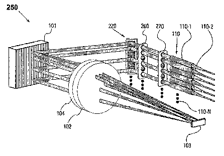
FIG. 2 depicts an alternative WSR apparatus 250 that may be used with
embodiments of the
present invention. By way of example, WSR apparatus 250 is built upon and
hence shares a
number of the elements described above with respect to FIG. 1A, as identified
by those
labeled with identical numerals. In addition to the components describe above,
the WSR
apparatus 200 further includes a one-dimensional array 220 of collimator-
alignment mirrors
(sometimes referred to as port mirrors) 220-1 through 220-N optically
interposed between the
diffraction grating 101 and the fiber collimator array 110. The collimator-
alignment mirror
220-1 is designated to correspond with the input port 110-1, for adjusting the
alignment of the
input multi-wavelength optical signal and therefore ensuring that the spectral
channels
impinge onto the corresponding channel micromirrors. The collimator-alignment
mirrors
220-2 through 220-N are designated to the output ports 110-2 through 110-N in
a one-to-one
correspondence, serving to provide angular control of the collimated beams of
the reflected
spectral channels and thereby facilitating the coupling of the spectral
channels into the
respective output ports according to desired coupling efficiencies. Each
collimator-alignment
mirror may be rotatable about one axis, or two axes. Settings for the
orientation of each of the
collimator alignment mirrors 220-1 to 220-N may be established from a set of
stored values
with each mirror set to a single position for optimum coupling to its
corresponding port.
The apparatus 250 may also include first and second two-dimensional arrays
260, 270 of
imagining lenses, which are placed in a 4-f telecentric arrangement with
respect to the two-
dimensional collimator-alignment mirror array 220 and the fiber collimator
array 220. By
way of example, the imaging lenses in the first and second arrays 260, 270 may
all have the
same focal length f. The collimator-alignment mirrors in the array 220 are
placed at the
respective first (or front) focal points of the imaging lenses in the first
array 260. Likewise,
the fiber collimators in the fiber collimator array 110 are placed at the
respective second (or
back) focal points of the imaging lenses in the second array 270. The
separation between the
first and second arrays 260, 270 of imaging lenses is 2f. In this way, the
collimator-
alignment mirrors are effectively imaged onto the respective entrance surfaces
(i.e., the front
focal planes) of the GRIN lenses in the corresponding fiber collimators. Such
a telecentric
imaging system substantially eliminates translational walk-off of the
collimated beams at the
output ports that may otherwise occur as the mirror angles change.
FIG. 3 shows another alternative WSR apparatus 300 that can be used with
embodiments of
the present invention. By way of example, WSR apparatus 300 is built upon and
hence shares
9
CA 02616046 2008-01-21
WO 2007/018758 PCT/US2006/024075
a number of the elements used in the apparatus of FIG. IA and FIG. 2, as
identified by those
labeled with identical numerals. In this case, the one-dimensional fiber
collimator array 110
of FIG. 2 is replaced by a two-dimensional array 350 of fiber collimators,
providing for an
input-port and a plurality of output ports. Accordingly, the one-dimensional
collimator-
alignment mirror array 220 of FIG. 2 is replaced by a two-dimensional array
320 of
collimator-alignment mirrors, and first and second one-dimensional arrays 260,
270 of
imaging lenses of FIG. 2 are likewise replaced by first and second two-
dimensional arrays
360, 370 of imagining lenses respectively. As in the case of the embodiment of
FIG. 2B, the
first and second two-dimensional arrays 360, 370 of imaging lenses are placed
in a 4-f
telecentric arrangement with respect to the two-dimensional collimator-
alignment mirror
array 320 and the two-dimensional fiber collimator array 350. The channel
micromirrors 103
must be pivotable biaxially in this case (in order to direct its corresponding
spectral channel
to any one of the output ports). As such, the WSR apparatus 300 is equipped to
support a
greater number of the output ports.
In embodiments of the present invention, the channel micromirrors 103 are
controlled by
servo-control loops that are integrated into optical switches, e.g., of the
types described above
with respect to FIG. lA, FIG. 2 and FIG. 3. FIG. 4A depicts a schematic
illustration of a
WSR-S apparatus according to an embodiment of the present invention. The WSR-S
apparatus 400 comprises a WSR apparatus 410 and a servo-control assembly 440.
The WSR
apparatus 410 may be substantially similar to the WSR apparatus 100 of FIG.
IA, the WSR
apparatus 250 of FIG. 2 or the WSR apparatus 300 of FIG. 3 or any other
embodiment in
accordance with the present invention. The servo-control assembly 440 includes
a spectral
power monitor 460, for monitoring the optical power levels of the spectral
channels coupled
into output ports 420-1 through 420-N of the WSR apparatus 410. By way of
example, the
spectral power monitor 460 may be coupled to the output ports 420-1 through
420-N by way
of fiber-optic couplers 420-1-C through 420-N-C, wherein each fiber-optic
coupler serves to
"tap off' a predetermined fraction of the optical signal in the corresponding
output port. The
servo-control assembly 440 further includes a processing unit 470, in
communication with
the spectral power monitor 460 and the channel micromirrors 430 of the WSR
apparatus 410.
The servo control assembly 440 may further include a non-volatile memory 450
which may
be programmed with instructions in the form of a program 480 that is readable
by the
processing unit 470. The memory 450 may be a non-volatile memory, such as a
read only
memory (ROM), disk drive, flash memory or the like.
CA 02616046 2008-01-21
WO 2007/018758 PCT/US2006/024075
The program 480 may implement a method of adjusting dither amplitude as
described below.
The program 480 may be implemented by using digital signal processing ( DSP)
firmware
using a logic chip such as a field programmable gate array (FPGA) as the
processor 470 and
memory 450. Although the program code 480 is described herein as being
implemented in
firmware and executed using an FPGA, those skilled in the art will realize
that the method of
dither amplitude adjustment could alternatively be implemented using hardware
such as an
application specific integrated circuit (ASIC) or other hardware circuitry.
Alternatively, the
program 480 may conform to any one of a number of different programming
languages such
as Assembly, C++, JAVA or a number of other languages. The processing unit 470
and
memory 450 may be part of a general-purpose computer that becomes a specific
purpose
computer when executing programs such as the program 480. As such, it should
be
understood that embodiments of the invention can be implemented, in whole or
in part, in
software, hardware or some combination of both. In one embodiment, among
others, the
program code 480 may include a set of processor readable instructions that
implement a
method having features in common with the method 700 of FIG. 7 or the method
800 of FIG.
8, both of which are described below.
The processing unit 470 uses the optical power measurements from the spectral
power
monitor 460 to provide feedback control of the channel micromirrors 430 on an
individual
basis, so as to maintain a desired coupling efficiency for each spectral
channel into a selected
output port. As such, the servo-control assembly 440 provides dynamic control
of the
coupling of the spectral channels into the respective output ports on a
channel-by-channel
basis and thereby manages the optical power levels of the spectral channels
coupled into the
output ports. The optical power levels of the spectral channels in the output
ports may be
dynamically managed according to demand, or maintained at desired values
(e.g., equalized
at a predetermined value) in the present invention.
By way of example, the processing unit 470 may apply an appropriate
alternating (or
"dither") control signal to a channel micromirror, in superposition with the
dc control signal
for maintaining the channel micromirror at a particular pivoting position.
This enables both
the optical power level of the corresponding spectral channel and the rate of
change in the
optical power level (or the time derivative of the optical power level) at the
instant
micromirror's pivoting angle to be obtained. In view of the exemplary coupling
efficiency
curve depicted in FIG. ID, the rate of change in the optical power level is
proportional to the
11
CA 02616046 2008-01-21
WO 2007/018758 PCT/US2006/024075
slope of the coupling efficiency curve, and is therefore useful in locating
the micromirror's
pivoting angle corresponding to the measured optical power level. It is also
useful in
determining the magnitude of the feedback control signal to be applied to the
channel
micromirror, so as to achieve the desired coupling efficiency in a most
effective manner.
FIG. 5 illustrates the well-lcnown process of dithering. A curve 502 in the
graph represents
the optical coupling to a particular collimator for a particular mirror as a
function of mirror
angle. Vertical squiggles 504 represent dithering of the mirror at a frequency
f for different
nominal mirror angles. In embodiments of the present invention, the amplitudes
of dither
signals for coupling each mirror to each different output port may be
different. These dither
amplitudes are adjusted as described above. The dithering of the mirror
produces a
corresponding oscillation in an optical coupling signal for the output port.
Horizontal
squiggles 506 represent the derivative with respect to mirror position of the
optical coupling
signal (the error signal). At peak coupling the frequency is 2f, while at non-
peak coupling the
frequency is f witli a phase shift of+/-180 degrees. At the peak coupling the
average error
signal is zero. The error signal is fed into a control loop (e.g., with a PID
controller) that
controls the mirror. The demodulated dither provides an error signal that can
be used in a
PID control loop to move the MEMS to optimal coupling. The PID controller
adjusts the
mirror angle in a way that optimizes the error signal for optimal optical
coupling to the
collimator.
The servo control assembly 440 typically includes one or more digital-to-
analog converters
(DACs) that convert digital information from the processing unit to open loop
voltages that
are applied to the channel micromirrors. The digital information corresponding
to the applied
voltages are referred to as DAC values. In embodiments of the present
invention, the
dithering amplitude for each micromirror is determined from stored DAC
settings used to set
the angle of the mirror to optically couple signals to the different output
ports. As part of the
optical alignment, the channel micromirrors 103 are positioned for optimal
coupling of the
optical path at each output port collimator. Corresponding open loop voltages,
or DAC
values are then stored, in non-volatile memory. FIG. 6 depicts an example of a
graph of
DAC value as a function of collimator (port) number for a given mirror in a
switch of the
type depicted in FIG. 1. The diamonds in FIG 6 represent stored DAC settings.
These DAC
settings can be fit to a polynomial curve as shown by the dashed line in FIG.
6. An equation
corresponding to the polynomial curve can provide information about the
stiffness of the
12
CA 02616046 2008-01-21
WO 2007/018758 PCT/US2006/024075
hinges used in the channel micromirrors 103. As described above, optimal
coupling of the
optical signal is achieved during operation by applying a small dither to the
MEMS mirror
and demodulating a sample of the light that is tapped off. Information about
the hinge
stiffness can be used to determine the appropriate dither amplitude for
optimal coupling to a
given port.
For example, it is often desired by the user of the WSS that the optical
perturbation caused by
the dither should be minimized. Contradicting requirements are that the dither
should be
small for stability and minimal optical perturbation and sufficiently large to
provide a useful
error signal for the control loop. These conflicting requirements can for the
control system be
reconciled using by calculating a slope based on stored alignment data. The
control system
design can be done using nominal mirror parameters. Using nominal parameters
the control
loop gain is adjusted to give a good response time with little or no overshoot
to a step
response. The gain can be adjusted by two parameters. One parameter is the
dither amplitude
and the other is a gain constant that multiplies the error signal. The dither
amplitude must be
large enough such that the optical disturbance is detected in the optical
channel monitor with
good signal-to-noise ratio and sufficiently small that it doesn't affect
customer data traffic.
Typically an optical disturbance of 0.5% at optimal coupling meets these
criteria. Once the
dither amplitude is chosen the gain constant is then adjusted to give a good
step response.
Using a nominal mirror with a nominal optical platform the dither amplitude is
adjusted to
meet this criteria and the resulting value in DAC counts is REF DITHER. In the
same
manner the collimator at the center of the range has the minimum mirror tilt
and on a nominal
optical platform will result in a slope of REF_SLOPE.
Based on the foregoing, a method has been developed to utilize DAC settings
such as
REF DITHER and REF_SLOPE and DAC setting versus port number information of the
type shown in FIG. 6 to set the dither amplitude of a given mirror for each
different port. A
general method 700 for adjusting dither amplitude of one or more MEMS mirrors
in an
optical switch is set forth in the flow diagram of FIG. 7. The optical switch
may be as
described above, e.g., generally including an input port, and an array of one
or more MEMS
mirrors that can be selectively optically coupled to one or more of N optical
input/output
(I/O) ports, where N is an integer greater than or equal to 3. The method
begins at 702 by
aligning the one or more MEMS mirrors to achieve nominal peak coupling at each
of the N
collimators. At 704, the DAC settings for positioning each mirror in an open
control loop as
13
CA 02616046 2008-01-21
WO 2007/018758 PCT/US2006/024075
a function of the selected collimator are stored to the memory 450 of the
apparatus 400. At
706, a dither amplitude DITHER(x) is determined for one of the MEMS mirrors
positioned to
couple optical signals to an output port at a position x for using the stored
DAC settings. For
example, for a given one of the mirrors, N signal values Sc may be determined
with each
signal value S,_ corresponding to a signal applied to the given mirror to
couple an optical
signal between the input port and a different one of the N output ports. The N
signal values
may be fit to a polynomial of a parameter corresponding to a position of an
output port (e.g.,
the port number). A slope of the polynomial may then be determined at a value
corresponding to a given output port. A dither amplitude for the mirror may
then be
determined based on the value of the slope. For the purpose of illustration,
determination of
only one dither amplitude for one mirror is discussed. However, those of skill
in the art will
recognize that the same dither amplitude determination may be repeated for
each mirror in a
one-dimensional or two-dimensional array of channel micromirrors.
The feasibility of this technique has been demonstrated on a WavePath 4500
model
wavelength selective switch (WSS) available from Capella Photonics of San
Jose, California.
In a design using a nominal MEMS mirror the slope the DAC count versus
collimator has
known reference value here denoted REF_SLOPE. Based on the control system
design the
reference dither amplitude will have a value denoted here as REF DITHER. The
data stored
in non-volatile memory are the DAC values for each plate of the MEMS mirror
for each
collimator location. These values are used to determine the dither amplitude
corresponding to
each port. During boot up the following steps are executed as illustrated in
the Flow diagram
of FIG. 8.
At 802 the DAC values are read from non-volatile memory. At 804 the
differential DAC
drive of the mirror at each collimator position is calculated. This results in
a vector that is
1 xN for N collimators. For example, the DAC settings as a function of port
number as
illustrated in FIG. 6 may be stored as described above. Table I is an example
of differential
DAC values for a MEMS channel mirror in a WavePath 4500 WSS having 10 ports.
Note
that the set of DAC values will, in general, be different for each channel
mirror.
14
CA 02616046 2008-01-21
WO 2007/018758 PCT/US2006/024075
TABLE I
collimator dy
1 5144
2 4180
3 3070
4 1754
400
6 -848
7 -2384
8 -3592
9 -4636
-5500
At 806, the DAC setting inforination from 804 is curve fit to a 3'd order
polynomial, e.g., of
the form:
5 (Eq. 1) a3 c3 + a2 c2 + al c + ao = DAC_VALUE(k), lc= 1:N,
where c is the collimator number. Note that in this case DAC_VALUE(k) is a
specific
example of the signal value Sc referred to above with respect to FIG. 7.
Fitting the N DAC
values to the polynomial requires determination of four unknown coefficients.
However if the
collimators are arbitrarily re-numbered starting from 0 the first coefficient,
aO, is immediately
10 known,
(Eq. 2) aO = DAC_VALUE(1).
What remains is to find three unknown coefficients from N>3 data points.
(Eq. 3) a3 c3 + a2 c2 + al c = DAC_VALUE(k) - ao, Ic=2:N
This is an over-determined set of equations and has a solution that results in
the least mean
square error curve fit. The above N-1 equations can be written in the familiar
matrix form
A-x = b, where A is an N x 3 matrix and b is an N x 1 vector and x=[a3 a2 al]T
are the
unknown coefficients. The solution is
(Eq. 4) x = (ATA)-tATb.
The matrix term (ATA)''AT is size 3xN made up of polynomial terms of the
collimator
numbers. This matrix is pre-calculated offline and stored in the code as three
row vectors
each size 1xN, (R3, R2, and RI).
The coefficients are calculated in firmware as the inner product a3 = R3 -b,
(Eq. 4) a2 = RZ -b, and a, = R, -b.
CA 02616046 2008-01-21
WO 2007/018758 PCT/US2006/024075
Those of skill in the art will be able to implement the matrix operations
described above as a
sequence of computer instructions.
By way of numerical example, based on the differential DAC values of Table I,
the
corresponding third order polynomial is of the form:
(Eq. 5) 10.256c3 - 164.85cz - 506.93c + 5791.1 = DAC_VALUE(k)
Once the coefficients are known the slope at each collimator is calculated at
808 as:
(Eq. 6) slope(x) = 3-a3 cz + 2-a2 c + a, , c= O:N-1
Those of skill in the art will recognize that form of slope(x) is just the
derivative of Eq. 4 with
respect to c.
By way of numerical example, based on the coefficients of Eq. 6, the
corresponding values of
slope(x) for the different collimators are as given in Table II below.
TABLE II
Collimator
number
(x) slope(x)
1 -806
2 -1043
3 -1219
4 -1333
5 -1386
6 -1377
7 -1307
8 -1175
9 -982
10 -727
Once slope(x) is known, the dither amplitude DITHER(x) at each collimator
position x may
be calculated at 810 from the previously determined values of REF DITHER and
REF SLOPE as:
(Eq. 6) DITHER(x) = REF_DITHER * slope(x)/REF_SLOPE
The calculations are described here for one channel micromirror but within the
WSS the
calculations are repeated for each mirror in the channel micromirror array
103.
An advantage of this method is that the dither amplitude can be tuned for each
mirror in a
large array rather than using a single fixed value. By adapting the dither
amplitude to the
16
CA 02616046 2008-01-21
WO 2007/018758 PCT/US2006/024075
specific mirror being controlled a wider range of MEMS process distribution
can be used.
Using a small dither on MEMS with weaker hinges maintains a smaller optical
disturbance
then if larger fixed dither amplitudes were to be used. From a control point
of view the small
signal gain of a weaker hinge is larger than a strong hinge and requires a
smaller loop gain.
Since the dither amplitude is part of the loop gain reducing the dither
amplitude compensates
for the loop gain for the weaker hinge.
While the above is a complete description of the preferred embodiment of the
present
invention, it is possible to use various alternatives, modifications and
equivalents. Any
feature described herein, whether preferred or not, may be combined with any
other feature
described herein, whether preferred or not. Therefore, the scope of the
present invention
should be determined not with reference to the above description but should,
instead, be
determined with reference to the appended claims, along with their full scope
of equivalents.
In the claims that follow, the indefinite article "A", or "An" refers to a
quantity of one or
more of the item following the article, except where expressly stated
otherwise. The
appended claims are not to be interpreted as including means-plus-function
limitations, unless
such a limitation is explicitly recited in a given claim using the phrase
"means for."
17