Note: Descriptions are shown in the official language in which they were submitted.
CA 02617179 2008-01-29
- 1 -
Method for making an acoustic transducer
Field of the Invention
The present invention relates to the manufacture of
acoustic transducers from composite materials. It
relates in particular to the field of sonar detectors
designed to detect objects located at a relatively
short distance from the detector.
Context of the Invention - Prior Art
To obtain an acoustic transducer operating at high
frequency, it is known to use composite materials
instead of solid ceramics. This is because the use of
composite materials, such as 1-3 composites, for
example to produce a transducer allows the production
of the corresponding acoustic sensor to be simplified.
Such a transducer may in particular be completely
included within a filling substrate, of the
polyurethane type for example, without it being
necessary to provide an empty space around the
nonactive faces that does not transmit pressure.
The appended figure 1 shows schematically the structure
of such a composite. This composite consists of ceramic
posts 11 of parallelepipedal shape, for example with a
square cross section of the order of 1 mmz, and a height
h. These posts are generally distributed over a plane
in the form of orthogonal rows and columns. The
mechanical integrity of the array of posts is provided
by filling the free spaces between the posts with a
suitable dielectric matrix (not shown in the figure).
To produce a transducer, all that is then required is
to deposit layers of conducting material 12, 13 on the
active surfaces of the piece of material used. The
transducer thus produced may be mounted on a layer 14
of absorbent or backing material.
CA 02617179 2008-01-29
- 2 -
A plate of composite material is obtained in a known
manner from a solid ceramic plate by machining parallel
channels of identical widths that lie along two
perpendicular directions. This double machining
operation makes it possible to form a simple structure
consisting of aligned posts 11.
A block of composite material such as that described
above is relatively easy to produce for working
frequencies of the order of megahertz. This is because
the height h of the ceramic posts to be produced is
then small, of the order of a few tenths of a
millimeter to one millimeter, which height is
relatively easy to obtain by machining a ceramic plate.
However, when a block of material suitable for a lower
acoustic frequency, of the order of 100 kHz for
example, has to be produced from a single ceramic
plate, two different technical problems arise.
The first problem encountered lies in the difficulty of
machining taller posts, needed to produce a composite
with a working frequency of the order of 100 kHz. For
such a working frequency, the height of the posts must
be several millimeters, but it is difficult to obtain
posts with a height of greater than 5 mm by machining.
In this case, in conventional machining techniques the
machined ceramics often break and a very high scrap
rate is observed.
The second important problem encountered when producing
low-frequency transducers from a composite material is
an electrical one. This is because, as shown in figure
1, such a transducer is electrically connected by means
of two metal plates 12 and 13 placed on the upper face
and on the lower face of the transducer. Each post can
then be considered as a capacitor, the capacitance of
which is given by the known general expression: C= Eh
CA 02617179 2008-01-29
- 3 -
where s represents the dielectric constant of the
ceramic used, h the height of the post and s its cross
section. Each post contributes to the capacitance of
the transducer through its individual capacitance.
Consequently, the capacitance of a transducer produced
from a composite material depends on the thickness of
the material, so that a low-frequency transducer will
have a lower capacitance than a higher-frequency
transducer. For a working frequency of the order of 100
kHz, the value of the capacitance presented by the
transducer is so low that it results in poor matching
impedance responsible for the appearance of electrical
noise, to the detriment of the overall operation of the
sensor.
The major drawback of using composite materials to
produce transducers operating at a frequency lying
around 100 kHz and with good sensitivity therefore lies
in the difficulty of producing the transducer and in
the limitation of its electrical characteristics, which
results in its performance being limited.
A known solution for producing a low-frequency acoustic
transducer from a material of 1-3 composite type of a
given area having both the desired height h and an
electrical capacitance value allowing the electrical
noise to be maintained at an acceptable level consists
in superposing two or more transducers of the same type
that operate at a given frequency and in connecting
them in parallel from the electrical standpoint.
The appended figure 2 illustrates the device
theoretically obtained in an ideal production
situation. It shows two identical transducers 21 and 22
represented schematically by their ceramic posts. The
two transducers are superposed so that the polarization
axes of the ceramic elements are oppositely oriented. A
plane metal electrode 23 is interposed in the plane of
contact between the two transducers. Two plane
CA 02617179 2008-01-29
- 4 -
electrodes are also placed on the faces 24 and 25
facing the plane of contact and electrically connected
together. In this way, from the electrical standpoint,
the two transducers 21 and 22 are connected in parallel
and their electrical capacitances are added.
Furthermore, the superposition makes it possible to
artificially produce a transducer comprising ceramic
posts 26 formed by the superposition of the posts 11
belonging to each of the transducers 21 and 22
respectively. The height H of each post 26 thus formed
is advantageously equal to twice the height h of each
of the assembled transducers 21 and 22. What is thus
obtained is a transducer having a working frequency
half that of the two transducers from which it is
formed.
The effectiveness of this solution, which is already
known, is dependent on the quality with which the
transducers are produced and superposed. This is
because, in order for the resulting transducer to
operate satisfactorily and have a single resonance peak
with an exploitable amplitude, it is necessary for the
superposition to be carried out sufficiently precisely,
so that, for a given row or column, the superposed
posts are strictly in alignment and their faces are
identically oriented. Now, the known methods of
producing composites used hitherto do not allow the
production of composites having sufficiently regular
arrangements of posts so that precise positioning of
all the posts facing one another after the
superposition of several transducers to be possible. In
practice, what is generally obtained, as illustrated in
figure 3, are transducers having an arrangement of
posts 31 in more or less straight rows and columns, but
the superposition of which has alignment imperfections
33 in the plane of superposition 32. The main
consequence of these imperfections is that they lead to
a misalignment of some of the reconstituted posts 34
formed by the superposition of the two transducers.
CA 02617179 2008-01-29
- 5 -
This misalignment is manifested by the appearance of
losses, and therefore by a great reduction in the
amplitude of the resonance peak at the desired working
frequency.
Presentation of the Invention
One object of the invention is to provide a method for
producing low-frequency transducers, which is suitable
for frequencies typically of the order of 100 kHz,
which is easy to produce on an industrial scale and
which does not have the drawbacks of the transducers
produced by simple superposition of existing
transducers. For this purpose, the subject of the
invention is a process for producing a block of low-
frequency piezoelectric composite material consisting
of superposed ceramic posts, the interstices between
which are filled with a dielectric material. This
process comprises the following steps:
- a step 1 of machining a ceramic block so as to
form an array of parallel bars of rectangular cross
section, held in place by a ceramic base;
- a step 2 of separating the ceramic block into two
identical half-blocks by cutting the initial block in a
plane perpendicular to the axis of the bars;
- a step 3 of producing a block of twice the
thickness by superposing and assembling the two half-
blocks, the superposition being carried out so as to
bring the bars of each of the half-blocks face to face,
a conducting layer being inserted in the plane of
superposition of the two half-blocks, the array being
held between two ceramic bases;
- a step 4 of forming rows of ceramic posts from
the bars, by making cuts in the ceramic block that are
perpendicular to the bars formed in the previous step;
- a step 5 of filling the cavities of the ceramic
block with a dielectric material;
- a step 6 of eroding the bases; and
CA 02617179 2008-01-29
- 6 -
- a step 7 of depositing a layer of conducting
material on the external faces of the block of
composite material thus produced.
This process advantageously makes it possible to
produce a very regular block of composite material as
it is produced from two superposable blocks comprising
bars of substantially identical profiles as they are
produced in one and the same operation from one and the
same initial ceramic block.
Once these two blocks have been superposed and
assembled, they now form only a single block, of twice
the thickness and already partially cavitied, which it
is easy to machine so as to form well aligned and
correctly superposed posts.
Advantageously, since the bars are machined so as to
remain attached to a layer or base of ceramic, the
spacing between the bars is kept constant, thereby
ensuring that all the bars are precisely superposed and
held in position during the operation of producing the
posts. This sandwich structure also has the advantage
of increasing the strength of the material while the
posts are being machined and of limiting the risks of
fracture. The ceramic layers are removed by erosion or
polishing only after the filling step.
Description of the Drawings
The features and advantages of the process according to
the invention will become clearly apparent in the
following description, illustrated by the appended
figures which show:
- figure 1, a schematic representation of a high-
frequency transducer produced from a block of composite
material;
CA 02617179 2008-01-29
- 7 -
- figure 2, a representation of an ideal transducer
produced by superposing two blocks of composite
materials;
- figure 3, an illustration of the problems posed by
the known methods of production;
- figure 4, an illustration of steps 1 to 4 of the
process according to the invention; and
- figure 5, an illustration of steps 5 to 7 of the
process according to the invention.
Detailed Description
The process according to the invention may be easily
described with the aid of the illustrations shown in
figures 4 and 5.
Considering firstly figure 4, to produce a low-
frequency transducer according to the invention the
procedure is as follows. During a first step, a number
of parallel grooves 42 are made in a piece of
piezoelectric ceramic of thickness h, so as to form an
array of parallel bars 43 held rigidly together by a
ceramic layer 44 or base, having a preferably small
thickness e. Thus an array of parallel bars is
obtained, the spacing of which is advantageously well
controlled. The grooves 42 may for example be produced
by sawing using a well-known technique (not described
here).
During a second step, the piece of ceramic thus
machined is cut into two identical blocks 46 and 47 in
a plane of cutting perpendicular to the axes of the
bars and depicted by the axis 45 in the figure. In this
way, two twin blocks are obtained which bars are
accurately superposable..
Next, during a third step, the two blocks thus obtained
are superposed and assembled, for example by bonding.
During assembly, a sheet of conducting material, the
CA 02617179 2008-01-29
- 8 -
area of which is greater than that of the blocks 46 and
47, is interposed in the plane of superposition between
the two blocks. The sheet of conducting material 48 is
positioned so that one of its sides lies outside the
block of material 49 thus produced. This block takes
the form of bars of thickness 2h held captive between
two ceramic layers 44 to which they are solidly
attached. These two ceramic layers advantageously
ensure that the bars are held in place.
During the fourth step, a series of mutually parallel
cuts is made in the block of material obtained in the
previous step, these cuts being along axes
perpendicular to the axes of the bars 43 that make up
the block of material. According to the invention, the
grooves thus formed preferably have a width equal to
that of the grooves 42 produced during the first step.
Thus, an array of ceramic posts 410 arranged in
strictly parallel identical rows 411 is obtained.
Advantageously, during this cutting step the bars are
held in position by the external layers 44 that border
them. In this way, the sawing operation is carried out
while minimizing the risks of fracture. Thus, in any
one row 411, the posts 410 are held in position at one
end by a ceramic layer 44 and at the other end by
ceramic strips 412 resulting from machining the opposed
layer.
As illustrated in figure 4, after this fourth step the
sheet of conducting material is cut into conducting
strips 413 connecting all the posts of any one row 411
together.
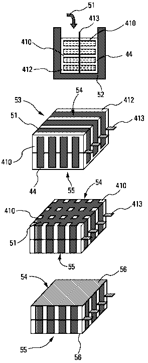
Figure 5 is now considered, which illustrates the rest
of the steps of the process according to the invention.
CA 02617179 2008-01-29
- 9 -
As illustrated in this figure, the fourth step is
followed by a fifth step that consists in filling the
empty spaces that separate the ceramic posts 410 from
one another, by pouring a dielectric material 51, for
example a polymer, between these posts.
The pouring is for example carried out via the face
from which the conducting strips 413 protrude, the
other faces being moreover closed off by means of a
tool 52 forming a box. As soon as the poured material
has solidified, the tool 52 is removed and the block 53
of composite material thus obtained is revealed.
Next, during step 6, this block of material undergoes
an operation of eroding the faces 54 and 55 that are
parallel to the plane of the conducting strips 413.
Owing to the small thickness of the ceramic strips 412
and of the ceramic layer 44, this operation may
advantageously be carried out by polishing the surfaces
in question. What is thus obtained is a block of
composite material that takes the form of an array of
ceramic posts 410 imprisoned in a matrix 51 of polymer
material.
The complete block of composite material is then
finished off during a final step 7. During this step,
each of the polished faces 54 and 55 is covered with a
layer 56 of conducting material, which operation may
consist in metallizing the faces 54 and 55. This layer
may be a continuous layer, as shown in the figure, but
it is also possible to produce, depending on the
envisaged use, more complex metallizations so as for
example to form parallel strips identical to the strips
413 buried within the material.
A block of composite material thus produced by the
process according to the invention advantageously has
in the end a structure substantially identical to the
structure shown in figure 2, which structure, as
CA 02617179 2008-01-29
- 10 -
mentioned above, is extremely difficult to obtain by
any known process.
Figure 6 is now considered, which clearly demonstrates
the advantages of producing a transducer from a piece
of composite material manufactured by the process
according to the invention.
As illustrated in figure 6, each column of
piezoelectric ceramic posts may be electrically wired
so as to connect the posts in parallel. In this form of
assembly, the.conducting elements 56 of the external
faces are electrically connected so as to form a
negative pole 62, whereas the internal conducting strip
413 forms a common positive pole 63. As indicated by
the arrows 61 in the figure, during manufacture of the
piece of composite material, the superposition of the
two ceramic elements 46 and 47 is carried out so that
the polarization directions of the two elements allow
this parallel mounting.
The advantage presented by such an arrangement is
considerable. Firstly, it makes it possible to produce
a transducer consisting of elements capable of
resonating at a lower frequency. Connecting the posts
in parallel in the arrangement illustrated by figure 6
places the superposed blocks in phase opposition, with
the consequence that the resonance of each post at its
eigen frequency is highly attenuated and that the
resonance of the assembly at half the frequency which
represents the desired resonant frequency, is
reinforced. This parallel mounting also makes it
possible, as was mentioned previously, for the
electrical capacitance of the assembly to be twice that
of a monolithic transducer of the same thickness.
The wiring diagram shown in figure 6 illustrates the
way in which each row of posts of a piece of composite
material produced by the process according to the
CA 02617179 2008-01-29
- 11 -
invention can be used to constitute a transducer. Each
of the rows may then be connected to the others so as
to form the complete transducer. The way in which the
various rows are connected together depends on the mode
of operation of the complete transducer and in
particular on the shape of the directivity pattern that
it is desired to produce. One simple way of making this
connection consists for example in connecting all the
rows in parallel. This way of operating is of course
not limiting.
The process according to the invention has been
described in the above paragraphs in the particular
case of producing a transducer having posts of
identical size. However, this example is not limiting
and it is possible, of course, to generalize the
process without departing from the context of the
claimed invention. For example, it is possible to
produce a structure such as that illustrated by figure
3, comprising posts 34 consisting of two posts 33 of
two different sizes. To do this, all that is required
is to introduce an intermediate step 2a in the process,
which takes place between step 2 and step 3, and during
which the thickness of one of the two half-blocks is
ground so as to give it a different thickness from that
of the other half-block. This operation may be carried
out by any appropriate means. In this way, the assembly
produced during step 3 becomes asymmetrical. In this
alternative embodiment, what is obtained is a structure
having posts whose capacitance corresponds to the sum
of the capacitances of the two posts constituting each
half-block, whereas the resonant frequency obtained is
then equal to the sum of the two frequencies divided by
4.