Note: Descriptions are shown in the official language in which they were submitted.
CA 0261E1147 2013-10-09
1
Electrooptical distance measuring device
The invention relates to an electrooptical distance measuring
device and a method for adjusting such a distance measuring
device.
Distance measuring devices in the form of hand-held measuring
devices or industrial sensors have long been known and are
commercially available. Their distance measuring range is up
to 200m and they are used, for example, in construction
surveying, for example for the 3-dimensional surveying of
rooms. For this purpose, a transmitter emits intensity-
modulated radiation, in general wavelengths in the visible
range being used, which facilitates the sighting of the
measuring points. The radiation is reflected or scattered by
the measured object and picked up by the receiver. The
distance to the measured object is obtained on the basis of
the phase position of the modulated radiation relative to the
transmitter.
Such a measuring device is disclosed, for example, in EP 0 701
702. In this device, a semiconductor laser emits light to an
object to be surveyed, this light being received again and
evaluated after reflection. The measuring receiver has an
optical system whose beam axis is oriented substantially
parallel to the transmission axis, deflection elements for
beam guidance or movable, trackable entry surface for the
measuring radiation being used in the close vicinity. In order
to realise a highly precise measurement with a low level of
extraneous light components, the received radiation must be
limited to the measuring radiation component. This can be
achieved by a suitable choice
CA 02618147 2013-01-18
WO 2007/017020
PCT/EP2006/006474
2
of the diameter of the detector surface of the receiver
relative to the focal distance of the optical system.
An advantageous lower ratio of diameter to focal
distance in this context makes the arrangement
sensitive with regard to the exact orientation and
requires adjustment of the components, for example
during manufacture, as can be realised by moveable
adjusting elements or corresponding adjusting
facilities.
An adjustable arrangement of transmitter and receiver
is disclosed in EP 1 351 070, in which an
electrooptical distance measuring system for large
measuring ranges comprising the optical transmission
axis and receiving axis arranged in parallel a distance
apart is described. The radiation source and a small-
area photodiode are mechanically connected rigidly to
one another via an essentially rigidly connected
circuit board assembly. The small-area photodiode is
electrically conductive and is fixed in position by
means of its electrical contacts on the circuit board
assembly so as to be temporarily adjustable. The
adjustment is therefore effected by a movement of the
photodiode relative to the circuit board assembly, the
photodiode being fixed after reaching the optimum
position. By means of this fixing step to be carried
out in the device, in which an individual electronic
component must be moved, manufacture is made more
complicated. In
particular, the photodiode cannot
already be mechanically fixed rigidly on the circuit
board. This prevents utilisation of the advantages of
surface-mounted devices which are soldered fully
automatically by standard machines directly onto the
conductor tracks, for example from points of view of
assembly and strength.
It is the object of the invention to provide an
CA 02618147 2013-10-09
3
electrooptical distance measuring device having an improved
design, increased stability and simplified assembly.
The invention predominantly relates to hand-held distance
measuring devices of the generic type according to the phase
or pulse transit time measuring principle and based on an
adjustability of receiver components by displacement of the
support element supporting these components. The measuring
receiver is fixed on a support element at least relative to
two directions of movement and hence translationally fixed.
Adjustments in these directions of movements are effected by
displacement of the complete circuit board relative to the
beam axis of the receiving optical system, the circuit board
also being capable of holding components of the evaluation
electronic system. Suitable support elements are, for example,
the circuit board or board which, in the form of printed
circuit or printed circuit board, can have conductor tracks
for the components and can be automatically assembled.
The fixing of the measuring receiver on the circuit board can
advantageously be effected as a so-called surface mounted
device. Here, the components have no wire connections but are
soldered directly onto the circuit board by means of
solderable connection surfaces. This results in a mechanically
strong connection which is robust with regard to environmental
influences.
If the receiving optical system is realised with a fixed
focus, the measuring receiver can be fixed in all
CA 02618147 2013-01-18
WO 2007/017020
PCT/EP2006/006474
4
three directions and hence rigidly on the support
element. Positioning need therefore be effected only
in the two directions of movement perpendicular to the
optical axis. After
adjustment is completed, the
circuit board or the support element can then be fixed,
for example by tightening of screws, adhesive bonding
or other fixing methods.
An alternative to a fixed focus is focussing by means
of a mirror or another deflection element which
lengthens or shortens the beam path to the measuring
receiver. The mirror
can be moved relative to the
measuring receiver so that the third degree of freedom
for focussing is achieved by this variable distance.
The focussing in this variant is thus independent of
the adjustment in the other two directions of movement
and can be carried out very simply in one axis before
the adjustment. The adjusted image can be clearly seen
only during or after the adjustment.
Limited direct adjustability relative to the support
element can be achieved by adjustability of the
measuring receiver in one direction of movement. Thus,
an optical system without a fixed focus can be used and
the focussing is effected by the movement with regard
to the remaining translational degree of freedom. One
possibility for such a movement can be realised by
mounting the measuring receiver on a free strip of the
printed circuit board. The printed part of the circuit
board on which the measuring receiver is arranged is
springy and can be pressed, for example, by a screw or
another adjusting element into the focus.
The advantages of these working examples are in
particular the possibility of fixing avalanche
photodiodes as a surface mounted device. These diodes
can therefore be automatically inserted in the same
CA 02618147 2013-01-18
WO 2007/017020
PCT/EP2006/006474
operation with the remainder of the electronics.
An advantageous development basically independent of
the specific fixing of the laser diode also provides
5 for the integration of a driver chip into the standard
design of a laser diode, for example by replacing the
photodiode chip by the driver chip. Here, the
same
housing can still be used, the contacts being assigned
as follows:
1) Ground
2) VCC voltage supply
3) Signal input
The transfer of the driver chip into the laser diode
housing results in various advantages:
Firstly, short pulses with high power can be produced,
which pulses permit a better measuring performance. In
order to produce such pulses having a pulse width of a
few 100ps, currents which are as high as possible must
be passed through the laser in a very short time. The
inductance of the circuit comprising driver and laser
is a limiting factor. Here, the
required voltage is
proportional to the inductance at a specified current
increase.
di
L.¨
dt
The voltage is limited by the semiconductor technology
used, i.e. the faster the technology, the smaller are
the possible voltages which can be used. By combining
driver chip and laser chip in a standard housing, the
inductance in the power circuit can be optimised in
this manner.
CA 02618147 2013-01-18
WO 2007/017020
PCT/EP2006/006474
6
Secondly, in the case of short pulses, the deflection
of extraneous radiation is always a problem so that
metallic screening chambers have to be constructed.
The use of the laser housing results in good screening
of the load circuit, so that the remaining assembly of
optical system and printed circuit is possible on
plastic modules.
The translational positioning of the measuring receiver
relative to the optical axis of the receiving optical
system is very easy to realise since the printed
circuit board is simply gripped on the outside or edge
and displaced. The board is
thus very easily
accessible for an adjustment device.
Owing to the high frequencies used, screening of the
electronics is generally necessary. Since, for
stability reasons, a module comprising metal is used
for holding the optical system, a screened chamber can
be formed together with the conductor tracks.
In general, an additional optical element is required
for optimum measurement over short distances, e.g. from
5cm. The solution according to the invention makes it
possible to mount this element on the photodiode after
assembly. Thereafter, the board is fixed on the optics
module or optics support and adjusted.
Below, working examples of the invention are explained
purely schematically in more detail with reference to
the drawing.
Fig.1 shows a
first working example of a distance
measuring device according to the invention;
Fig.2a-b shows schematic detailed views of the first
working example;
Fig.3a-b show figurative detailed views of the first
CA 02618147 2013-01-18
WO 2007/017020
PCT/EP2006/006474
7
working example
Fig.4 shows a schematic detailed view of a second
working example of the distance measuring
device according to the invention and
Fig.5 shows a schematic detailed view of a third
working example of the distance measuring
device according to the invention.
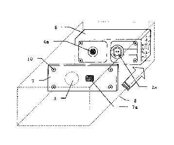
Fig.1 shows a first working example of an
electrooptical distance measuring device 1 according to
the invention, comprising a laser diode 2 as a
transmitter, which emits optical radiation or laser
light via a transmission optical system 3 having a
transmission axis SA for illuminating a measured
object. The light reflected by the measured object is
received by a receiving optical system 4 having a
receiving axis EA and passed to a measuring receiver 5,
e.g. an avalanche photodiode. The transmission axis SA
and the receiving axis EA are oriented parallel or with
only a slight inclination relative to one another, so
that the arrangement within the measuring range has a
character of beam paths offset parallel relative to one
another. The
transmission optical system 3 and the
receiving optical system 4 can advantageously be
arranged on a common optics support 6 which can also
hold the laser diode 2 and fix it rigidly relative to
the transmission optical system 3_ In this
working
example, the emission axis of the laser diode 2 is
coaxial with the transmission axis of the transmission
optical system 3.
A first support element having transmission electronics
is assigned to the laser diode 2, and a second support
element having receiving electronics is assigned to the
measuring receiver 5, the two support elements being in
the form of a single circuit board 7 as a common
support element in this working example. The measuring
CA 02618147 2013-01-18
WO 2007/017020
PCT/EP2006/006474
8
receiver 5 is rigidly connected to the second support
element or the circuit board 7 with respect to at least
two directions of movement, completely rigid fastening
with fixing of all degrees of freedom relative to the
circuit board 7 being effected in this working example.
In the formation as a surface mounted device, the
fastening is effected directly and with final fixing on
the conductor track. In this
working example, an
opening 7a or a passage through which the contact
elements 2a of the laser diode 2 are led is
additionally formed in the circuit board 7. While the
laser diode 2 is fixed on the optics support 6 and is
therefore positioned in a defined manner relative to
the transmission optical system 3, the measuring
receiver 5 can be displaced by a movement of the
circuit board 7 relative to the receiving axis 3a and
adjusted thereby. In this
working example, the
receiving optical system 4 is formed with a fixed focus
so that it is possible to dispense with focussing
adjustment of the measuring receiver 5. The optics
support 6 with its components and the circuit board 7
are arranged, together with further components 9, such
as, for example, the power supply, in a housing 8 of
the distance measuring device 1. After adjustment is
complete, the axis of the measuring receiver 5 and the
receiving axis of the receiving optical system 4 are
aligned substantially coaxially.
The adjustment according to the invention for the first
working example is explained in fig,2a-b in schematic
detailed views.
Fig.2a shows a situation in which the receiving axis EA
and the optical axis or the midpoint of the measuring
receiver 5 are not in coincidence. By displacing the
circuit board relative to the optics support 6, the
situation shown in fig.2b with the alignment of the
CA 02618147 2013-01-18
WO 2007/017020
PCT/EP2006/006474
9
measuring receiver 5 with the receiving axis EA can be
achieved. After
positioning is complete, the circuit
board 7 can be fixed on the optics support 6. The
laser diode 2 is decoupled from the displacement of the
circuit board 7 by the opening 7a in the circuit board.
After adjustment is complete, the contact elements 2a
of the laser diode 2 are connected to the circuit board
7 and the transmission electronics arranged thereon.
In this example, the fixing of the common circuit board
7 is effected relative to the optics support 6.
According to the invention, however, it is also
possible to use two separate circuit boards for laser
diode 2 and measuring receiver 5. Direct fixing of the
circuit board 7 to the receiving optical system 4 or
indirect fastening via the housing 8 is also possible.
If a possibility of movement of the circuit board 7 in
the direction of the receiving axis EA is also
realised, the fixed focus can be dispensed with and
focussing of the measuring receiver 5 can be achieved.
Fig.3a-b illustrate the design of the first working
example by means of figurative detailed views. For
presentational reasons, only the circuit board 7 and
the optics support 6 are shown in the housing 8. A
receiving opening 4a of the receiving optical system 4
and the back of the laser diode with the contact
elements 2a can be seen on the back of the optic
support 6, which is visible in fig.3a. sores 10 for
connection of these components by means of screws are
made in the circuit board 7 and the optics support 6,
this connection being designed so that displaceability
of the circuit board 7 relative to the optics support 6
still exists prior to tightening of the screw
connection. The circuit board 7 is basically adjusted
to such an extent that the contact elements 2a are
flush with the opening 7a and the measuring receiver 5-
arranged here on the opposite side of the circuit board
CA 02618147 2013-01-18
WO 2007/017020
PCT/EP2006/006474
7- is flush with the receiving opening 4a.
Fig.3b shows the distance measuring device during the
adjusting process. Circuit board 7 and optics support
5 6 are connected to one another, the contact elements 2a
being led, with a play sufficient for the adjustment,
through the opening 7a of the circuit board 7. The
measuring receiver 5 is adjusted with respect to the
receiving axis by lateral displacement of the circuit
10 board 7 relative to the optics support 6.
Fig.4 and fig.5 show two alternative working examples
of a distance measuring device according to the
invention.
Fig.4 shows a schematic detailed view of a second
working example having a measuring receiver 5' moveable
perpendicular to the circuit board 7'. In this working
example, the receiving optical system 4' is not formed
with a fixed focus so that positioning of the measuring
receiver 5' with focussing is required. The measuring
receiver 5' is fixed in two directions of movement
relative to the circuit board 7'. In the third
direction of movement, however, it can be moved,
spring-mounting on a resilient element 11, e.g. a free
conductor track, being effected. The
measuring
receiver 5' is rigidly arranged on the conductor track
itself with regard to all directions of movement and is
finally fixed during the assembly itself. The
adjustability in one dimension or the focusability is a
result of the springy mobility of the conductor track
relative to the circuit board. The precise
displacement and fixing are permitted by way of example
by a grub screw 12. By means of this development, the
measuring receiver 5 can be positioned perpendicular
to the receiving axis EA by displacement of the circuit
board 7', the focussing being effected by adjustment of
CA 02618147 2013-01-18
WO 2007/017020
PCT/EF2006/006474
11
the grub screw 12.
Fig.5 shows a third working example having a deflection
mirror 13 suitable only for focussing or another
optical deflection element for a receiving optical
system 4" without a fixed focus. Once again,
the
measuring receiver 5" is fixed on the circuit board
7", which is now angled, in this working example all
degrees of freedom of the measuring receiver 5"
relative to the circuit board being reduced and a fixed
connection existing. Because the
movement of
deflection mirror 13 and circuit board 7" can be
decoupled and are thus independent of one another, both
positioning perpendicular to the receiving axis EA and
focussing can be achieved. Depending on the specific
design features, such as, for example, size of the
receiving surface of the measuring receiver 5", the
relative movement of mirror 13 and measuring receiver
5" can be permitted in different directions, which is
illustrated in fig.5 by a dashed arrow.
The working examples shown in the figure are not to be
understood as being definitive. In particular,
individual features can be combined with one another.
Thus, divided circuit boards or those which have
different angles or uneven progressions, which adapt,
for example, to corresponding developments of the
housing, can also be used. The fixing of the circuit
board or of another support element by means of
differently formed clamping, soldering or adhesive
bonding techniques can also be effected.