Note: Descriptions are shown in the official language in which they were submitted.
CA 02619338 2008-02-12
WO 2007/021436 PCT/US2006/028117
DIRECT'IONAL POWER DETECTION BY QUADRATURE SAIvIPLING
INTRODUCTION
FIELD OF THE INVENTION
[0002J The present invention relates to signal transmissions and, in
particular, to
measurement and control of signal transmission power.
BACKGROUND
[0003] In order to have power measurement and control, transmitters are
configured with
power control feedback loops responsive to power detectors. In conimon
configurations for high
(e.g., microwave) frequency bands, the power level is measured by a detector
in a waveguide
which is connected between the output of the power amplifier and the load.
[00041 In general, waveguides are used for transporting high frequency
signals, in part
because of their low-loss characteristics and ability to handle high power.
Waveguide
components are configured in a number of geometries, examples of which include
'parallel' with
a pair of plates, 'co-planar' with a thin slot in the ground plane of one side
of a dielectric
substrate with or without a conductor in the slot, 'dielectric' with a
dielectric ridge on a
conductor substrate, 'ridge' with conducting ridges on the top and/or bottom
walls, and
'rectangular' with a parallel-piped structtu=e of a stibstantially rectangular
cross section. Thus,
although the discussion here examines rectangular waveguides, other waveguide
may be suitable
for power measurement.
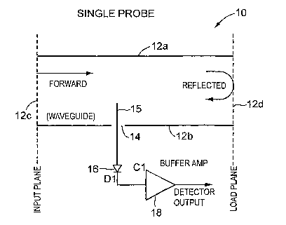
[00051 One approacli to power measurement can be described as the single probe
approach, as shown in Figure 1. The waveguide component is defined by its top,
bottom, input
and load planes, 12a-d, respectively. The waveguide has a single slot 14 in
the bottom plane and
Pagelofl9
CA 02619338 2008-02-12
WO 2007/021436 PCT/US2006/028117
ff.a snngte.,proDa f~ti~,,.rqr i~'g the power level protrudes into the
waveguide tluough this slot
14. The probe 15 is often made of a conductive material and the potential
generated tliereby
drives the detector diode 16. The output of the detector diode 16 is coimected
to a buffer
amplifier 18 in order to isolate the detector diode from downstream components
(not shown) and
prevent their interference with its signal integrity.
[0006] As shown, fonvard signals traverse the waveguide fonn the input plane
12c to the
load plane 12d. Ideally, there would be a perfect impedance match between the
waveguide and
the load (antenna or test equipment not shown) and the entire sig7ial energy
would be transferred
from the waveguide to the load. In reality, however, the match is imperfect
and results in
reflections of the fonvard signals from the.load plane 12d. The opposite-
traveling reflected
signals interfere with the forWard signals and this produces a new wave
pattern lcnown as
standing waves, which is what the probe 15 ultimately measures.
[0007] The amplitude of the standing waves is effected by the degree of
interference of
the reflected signals with the forward signals which is based on the degree of
mismatch between
the waveguide and the load. Then, because with the single probe configuration
there is no
isolation from the load mismatch, this measurement is strongly influenced by
variations in the
load conditions.
[0008] A second approach, described as a directional waveguide coupler,
attempts to
solve the problems associated with the unreliable power measurement inherent
in the single
probe configuration. Figure 2 illustrates the directional waveguide coupler.
[00091 The directional waveguide 21 is designed for a particular frequency
band with
top, bottom, input and load planes 22a-d, respectively, and with the slots 24a
and 24b in the
bottom plane 22b spaced apart a quarter wavelength (or 90 ). Attached to the
bottom plate of the
waveguide and facing the slots 24a and 24b is a coupler 23, also configured as
a. waveguide. The
coupler 23 has a waveguide tern-iination plate 26 and a bottom plate 25 with a
slot 28 through
which the power probe 29 protrudes. As before, the power probe 29 is connected
to a detector
diode 32 which is, in turn, connected to the buffer amplifier to produce the
detector output while
isolating it from downstream stages.
Page2of19
CA 02619338 2008-02-12
WO 2007/021436 PCT/US2006/028117
~~d~h(~.}i(C1Tnd"e~::~C~,t~a](,1q(a~'~~~onditions there would be a perfect
match between the
waveguide and the load (antenna or test equipment not shown), and the load
plane 22d Nvould
transfers the forward signals from the waveguide to the load without losses.
In,reality, the load
conditions are not perfect because of the load-waveguide impedance mismatch
and the load
plane 22d reflects the forward signals. The reflected waves interfere with the
forward waves and
wlienever two waves of similar frequency travel in a medium in opposite
directions standing
'waves are formed. Thus, the load plane acts as a constructive or destructive
reflector based on its
position relative to the resultant standing waves cycle. The same applies to
the signals passing to
the coupler tlirough the slots 24a and 24b.
[0011] The forward signals that pass tlirough slots 24a and 24b, respectively,
converge at
the probe 29 in phase. This is because the fonvard signals moving through the
waNteguide 21 and
slot 24b and those moving through slot 24a and the coupler 23 travel the same
respective quarter
wavelength (90 ) distance. At the same time, reflected signals which pass
through slot 24a travel
the quarter wavelength (90 ) distance tvice, once in the direction toward slot
24a and once in the
opposite direction toward the probe 29. In other words, reflected signals that
pass through slot
24a are 180 out of phase relative to the reflected signals that pass through
slot 24b.
[0012] It is noted that a fiill cycle of the wave is comparable to a full
circle of 360 , and
any fraction of the circle in degrees is comparable to a fraction of the wave
cycle which is the
phase. When the forward and reflected signals are in -phase (0 or 360 phase
difference), the
interference is constructive and produces a. stariding wave which is the sum
of both (with twice
the amplitude); and the interference is destructive when they are out of phase
from each other.
The phase shift (P) between the opposite-traveling waves can be 0<P>360 ,
where a 1 80 phase
shift results in mutual cancellation of these waves.
[0013] Thus, the reflected signals converge at the probe 29 at 180 out of
phase and
cancel each otlier. Ideally, the probe 29 reads the magnified fomiard signals
and none of the
reflected signals. In reality, however, there is an imperfect match at the
waveguide termination
plate 26 and some of the reflected signals do end up converging at the probe
with less or more
than 180 phase shift.
Page 3 of 19
CA 02619338 2008-02-12
WO 2007/021436 PCT/US2006/028117
1I[,66;Itj imperfection is any inaccuracy in the complex mechanical
structure of the waveguide and coupler. Indeed, any variation in the operating
frequency and/or
the mechanical dimensions or material of the waveguide and coupler components
can create a
mismatch and, as a result, introduce some of the reflected waves at the probe
29. In particular,
the frequency dependent waveguide termination plate design calls for different
types of material
to achieve the desired perfomlance. Moreover, manufacture of the waveguide and
coupler
involves non-flexible frequency-dependent mechanical and electrical design for
achieving
performance such as isolation and power cotipling. The two-part directional
waveguide stnicture
is hard to build and is even harder to replicate in comrnercial quantities.
SUMMARY
[0015] In view of .the foregoing, the present invention proposes solutions
that address this
and related issues. These solutions include systems, devices and niethods that
are'provided in
accordance with the principles and variotis embodiments of the present
invention.
[0016] As shown and broadly described herein, one embodiment is a device for
power
detection. This device includes a waveguide, a pair of probes, a quarter
wavelength delay
component, a power combiner, a detector diode and a carrier on which the pair
of probes, quarter
wavelength delay component, power combiner and detector diode are laid out.
The waveguide is
configured for transporting forward and reflected waves of a signal with a
corresponding
wavelength and a power level. For the purpose of power detection, the
waveguide has a pair of
slots spaced apart by a quarter of the wavelength. The pair of probes protrude
into the waveguide
through the pair of slots for probing the signal and measuring its power
level. The pair of probes,
quarter wavelength delay component, power combiner and detector diode are laid
out on the
carrier in a configuration where the forward waves converge at the power
combiner
constructively and the reflected waves converge at the power combiner
destructively. This way,
the power measurement is substantially independent from load condition
variations.
[0017] It is noted that the carrier is a printed circuit board or a substrate.
The substrate
can be integrated into an integrated circuit or any other suitable
coiifiguration for high frequency
(particularly microwave) applications. In the case where the carrier is a
substrate it may or may
Page 4 of 19
CA 02619338 2008-02-12
WO 2007/021436 PCT/US2006/028117
the circuit components that need to be, sucli as the probes, are
properly exposed to the waves.
[0018] Typically, the waveguide has top, bottom, input and load planes,
wherein the pair
of slots are located in the bottom plane such that one of the slots and, in
turn, one of the probes,
are closer to the input plane. In this case, the configuration is one in which
the detector diode is
connected to the power combiner for receiving a signal proportionate to the
measured power
level and in which the power combiner is connected to the pair of probes. One
side of the power
combiner is connected via the quarter wavelength delay compori.ent to the
probe which is closer
to the inptrt plane.
[0019] Another device for power detection is configured with a pair of members
and a
detection circuit carrier. In particular, the pair of members are detachably
joined to form a body
with a duct, wherein the duct defines a waveguide for transporting forward and
reflected waves
of a signal with a corresponding wavelength and a power level. As before, the
waveguide has a
pair of slots spaced apart by a quarter of the wavelength. The detection
circuit carrier is inserted
between the joined pair of members and fits removably therebetween. The
detection circuit
carrier has a pair of probes, a quarter wavelength delay component, a poiver
combiner, and a
detector diode, wherein the pair of probes protrude into the waveguide through
the pair of slots
for probing the signal and measuring its power level. Moreover, the pair of
probes, quarter
wavelength delay component, power con-ibiner and detector diode are laid out
on the detector
circuit carrier in a configuration where the forward waves converge at the
power combiner
constructively and the reflected waves converge at the power combiner
destructively, whereby
the power measurement is substantially independent from load condition
variations. Again, the
detector circuit carrier is a printed circuit board or a substrate as
explained above.
[0020] In yet another enlbodiment, a power detection and control loop in a
transmission
system includes a waveguide between an output stage and a load, a detector
circuit for measuring
the power level substantially at the load and a control circuit, The output
stage produces a signal
with a corresponding wavelength and power level, and the waveguide transports
forward and
reflected waves of the signal. Again, the waveguide has a. pair of slots
spaced apart by a quarter
of the wavelength. The detector cireuit is laid out on a circuit carrier and
has a pair of probes, a
Page5of19
CA 02619338 2008-02-12
WO 2007/021436 PCT/US2006/028117
qLt~arter ct~r.riponent, a power combiner, and a detector diode, wherein the
pair
of probes protrude into the waveguide through the pair of slots for probing
the signal and
measuring its power level. The pair of probes, quarter wavelength delay
component, poNver
combiner and detector diode are laid out on the detector circuit carrier in a
configuration where
the fonvard waves converge at the power combiner c=onstruc=tively and the
reflected waves
converge at the power combiner destructively, whereby the power measurement is
substantially
independent from load condition variations. The control circuit has a buffer
amplifier lii-flced to
stages responsive to the measured power level and operatively linked to the
output stage for
controlling its gain and, in turn, the power level of the signal.
Incidentally, the load is an ant.eiina
or a dumrny load in a test device and, as before, the circuit carrier is a
printed circuit board or a
substrate.
[0021] In accordance with yet another embodiment of the invention, a method
for
detecting power in a transmission system includes a number of steps. One step
involves inserting
a waveguide between an output stage and a load for transporting forward and
reflected waves of
a signal with a corresponding wavelength and a power level. For this method,
as with the devices
above, the waveguide has a pair of slots spaced apart by a quarter of the
wavelength. Another
step involves inserting, through the pair of slots, a pair of probes into the
waveguide, the pair of
probes being capable of probing the signal and measuring the power level.
Another step is where
a quarter wavelength delay component is introduced 'ulto a measured signal
path between a first
one of the pair of probes and one side of a power combiner, the other side of
the power combiner
being directly comiected to the a second one of the pair of probes. Then,
another step involves
detecting a signal proportionate to the measured power level, the signal being
detected by a diode
which receives the signal from the power combiner. Once again, the pair of
probes, the quarter
wavelength delay component, the power combiner and the diode are laid out on a
circuit carrier
in a configuration where the forward waves converge at the power combiner
constructively and
the reflected waves converge at the power combiner destructively, whereby the
power
measurement is substantially independent from load condition variations.
[0022] In accordance with yet another embodiment, a method for detecting and
c.ontrolling power in a transmission system includes the step of inserting a
waveguide between an
otitput stage and a load for transporting fonvard and reflected waves of a
signal with a
Page6of19
CA 02619338 2008-02-12
WO 2007/021436 PCT/US2006/028117
"~o~r~spbYidYif~'f~'~avcfefi'~tIK ahd'''a power level. As with the preceding
embodiments, the
waveguide has a pair of slots spaced apart by a quarter of the wavelength.
This method further
includes the step of inserting, through the pair of slots, a pair of probes
into the, waveguide. This
is so that the pair of probes can probe the signal and measure the power
level. This method
additionally includes the step of introducing a quarter wavelength delay
component into a
measured signal path between a first one of the pair of probes and one side of
a power combiner,
the other side of the power combiner being directly coiinected to the a second
one of the pair of
probes. With this approach, a signal proportionate to the measured power level
is detected. The
signal is detected by a diode which receives the signal from the power
combiner. In this instance,
as in the others, the pair of probes, the quarter wavelength delay component,
the power combiner
and the diode are laid out on a circuit carrier, a printed circuit board or a
substrate, in a
configuration where the fonvard waves converge at the power combiner
constructively and the
reflected waves converge at the power combiner destructively. This way, the
power
measurement is substantially independent from load condition variations. The
detected signal is
fed to downstream stages that are operatively linked with the output stage to
control its gain and,
in turn, the power level in response to the measured power level.
[0023] Orie benefit derived from the present invention as broadly described
herein is
si-inplicity of implementation. Another benefit derived from the present
invention is lower cost to
manufacture for commercial applications. And, even with this simpler
configuration, the present
invention advantageously provides a more reliable power measurement and
control. In stun, these
and other features, aspects and advantages of the present invention v,rill
become better understood
from the description herein, appended claims, and accompanying drawings as
hereafter
described.
BRIEF DESCRIPTION OF THE DRAWINGS
[00241 The accompanying drawings which are incorporated in and constitute a
part of
this specification illustrate various aspects of the invention and together
with the description,
serve to explain its principles. Wlierever convenient, the same reference
numbers will be used
throughout the drawings to refer to the same or like elements. The drawings
include:
Figure 1 illustrate a conventional single probe configuration;
Page 7 of 19
CA 02619338 2008-02-12
WO 2007/021436 PCT/US2006/028117
"141glH 'ILI""i'11ti'sti"a'te a'-conventional directional waveguide coupler
configuration;
Figure 3 illustrates a directional waveguide power detector configured in
accordance with
an embodiment of the present invention; and
Figure 4 is a perspective view of the directional waveguide of Figure 3.
DETAILED DESCRIPTION
[0025] The present invention is based, in part, on the obsentation that
transmitters of
radio frequency signals are calibrated for particular load conditions. In a
typical situation, a
transmitter is calibrated with test equipment as the load and then used with
an antenna as the
load. The load conditio.ns created by the test equipment are not necessarily
exactly the same as
the load conditions created by the antenna, and, moreover, different antennas
have slightly
different characteristics and may create different load conditioris at the
output of the transmitter.
In some situations, the manufacturer may calibrate the transmitter with one
kind of test
equipment and a compliance verification laboratory may test the transmitter
with another kind of
test equipment (e.g., for FCC rules compliance). Transmitter load conditions
may vary also with
environmental changes such as temperatures and humidity variations. For this
reason the present
invention looked at ways to substantially overcome variations in load
conditions and thereby
improve power meastirement and control in transmission systems. We will exan-
iine such ways
with the examples that follow.
[0026] In general, because it recognizes that load conditions are iniperfect
and often
result in standing waves produced from reflected signals interfering with
forward signal, the
present invention proposes to substantially cancel the effects of the
reflected waves. Specifically,
the present invention proposes to converge reflected waves which are out of
phase at
substantially 1 S0 and thus cancel each other.
[0027] One approach for implementing this involves quadrature sampling in a
directional
waveguide. Figure 3 illustrates a'directional waveguide for power detection by
quadrature
sampling.
[0028] As shown, the power detection system 100 includes a directional
waveguide
defined by top, down, input and output planes, 102a-d, respectively. The
bottom plane 102b has
PageSof19
CA 02619338 2008-02-12
WO 2007/021436 PCT/US2006/028117
""'tWo''slbTs~ 104~ '~hd 1-04b sp'aced apart a quarter wave distance (90 ),
based on the frequency
band. Two probes 106a and 106b (labeled P1 and P2, respectively) protrude
through the slots
into the waveguide. The probes are therefore also spaced apart and quarter
wave distance, or 90 .
The physical dimensions of the waveguide and, in particular, the distance
between the slots 104a
and 104b depend on the frequency range of transmission. Thus, for instance, if
the transmission
frequency is 50GHz and the bandwidth that is 101'//0 of the transmission
fi=equency, i.e., +/-
2.5GHz, a quarter wavelength would be a 1.5mni.
[0029] In this configuration, the probes, P1 and P2, are passive devices such
as
conductors (traces) on a printed circuit board (PCB) 120. The PCB is shaped to
allow passage of
the two probes through the slots 104 a and 104b. Then, in addition to the
probes, the PCB 120
holds detector circuit components such as a 90 delay line 108, a power
combiner 110 and a
detector diode 112. The power detector circuit on the PCB is fonned with the
probe P1
connected to one side of the power combiner via the 90 delay line and with
the probe P2
connected to the other side of the power combiner. The detector diode 112 is
connected across
the power combiner 110 to receive a signal which represents the measured
power. The power
combiner in this circuit is a passive circuit such as a resistive connection
that produces a voltage
drop proportionate to the current induced from the power meastired by the
probes P 1 and P2.
[0030] The buffer amplifier 114 and downstream stages (not shown) are located
off the
PCB 120. The buffer amplifier protects the detector diode from the effects of
downstream stages
in order to maintain the diode's signal integrity and reliably correlate the
output of the diode with
the measured power.
[0031] In operation, the forward signals are any type of transmitted signals
at a particular
frequency range, having a particular power level and being modulated if they
carry any
infonnation. Un-modulated signals with a particular frequency do not contain
any inforn-iation
and they are typically lcnown as the carri.er waves. Modulated signals carry
information and they
are created by various modulation techniques examples of which include AM
(amplitude
modulation), FM (frequency naodulation), QAM (quadrature amplitude
modulation), and PWM
(pulse width modtilation). The forward signals travel from the input plane
102c toward the
output plane 102d and because of imperfect load conditions reflected signals
travel in the
Page9of19
CA 02619338 2008-02-12
WO 2007/021436 PCT/US2006/028117
bop6sh~~Ui4~6dt31ori.0dth~faf1A7drd and reflected signals are intercepted by
the probes P1 And P2,
which are located 90 apart, and converge at the power combiner:
(0032] As they travel tlirough the waveguide, fonvard waves intercepted by
probe P 1
pass through the 90 delay line and thus incur a 90 delay. At the same time,
forward signals
intercepted by probe P2 pass directly to the power combiner, but they incur a
90 delay in
reaching probe P2 because of the 90 distance between probe P 1 and P2. In
other ~arords,
because they are equally delayed by 90 , the forvvard signals intercepted by
probes P1 and P2
converge at the power combiner in phase relative to each other. This means
that the fonvard
signals' convergence is constrtictive and the resulting signal is the sum of
both.
[0033] By comparison, the reflected signals converge at the power combiner at
opposite
phases (180 ) relative to each and their convergence is destructive. More
specifically, reflected
waves intercepted by probe P2 pass directly to the power combiner while
reflected waves
intercepted by probe Pl travel 1SO before they reach the power combiner (90
distance to PI and
90 delay at the delay line). Signals converging at 1 SO phase difference
cancel each other.
Therefore, the destructive convergence of the reflected signals results in
them canceling each
other and not effecting the power measurement. In other words, the measured
power as presented
by the voltage across the power combiner is substantially free from load
condition variations.
The measured power is then reliably detected by the detector diode 112 and the
value is passed
along via the buffer amplifier 114 to downstream stages (of the power control
loop).
[0034] It is noted that the frequency range is scalable to other, higher
frequencies simply
with changes to the PCB layout design and changes to the waveguide dimensions
and distance
betueen the slots. In essence, there wauld be one set of dimensions for each
frequency, but the
fundamental design is similar for the various frequencies. The ease with which
a PCB can be
designed and made is one advantage of the present invention.
(0035] It is further noted that the depth of insertion of the probes into the
waveguide
controls the sensitivity of the detector circuit (i.e., the power level
detection voltage at the power
combiner). Hence, the ease with which the PCB can be adjusted to achieve the
proper depth of
protrusion into the waveguide is yet another advantage of the present
invention. Furthemiore, the
PCB can be made sufficiently small that it fits easily inside the waveguide
body.
Page 10 of 19
CA 02619338 2008-02-12
WO 2007/021436 PCT/US2006/028117
1-UU0301 "r'rgu7 6141'i~s+--aft. i~~ometne view of a waveguide, taken apart,
and a PCB with the
power detection circuit. In this illustration, the waveguide is produced when
the two semi-
circular members lOla and 101b are joined. The material these members are made
out of is
suitable for microwave applications and is therefore suitable for producing
the waveguide. When
joined, the two members form a cylinder with a duct which, in this case, has a
rectangular cross
section and is substantially aligned with the axis of the cylinder. The length
of the cylinder
determines the leiigth of the duct and, in turn, the length of the waveguide
(as necessary for the
particular frequency band). The shape and dimensions of the duct define the
walls of the
waveguide and particularly the top, bottom, input and load planes 102a-d. The
bottom plane
102b has two notches.that define the slots 104a and 104b tiu-ough which the
probes 106a and
106b can protrude into the waveguide. Being smaller than the length of the
waveguide, the
distance between the slots, and in turn the probes, is set to a quarter
wavelength (90 ) which
varies with the transmission frequency band. One or both members accommodate
the PCB and
the slots. Specifically, one or both members 101and lOlb have a detector notch
extending below
the bottom plane (not shown) for fitting the PCB with the power detection
circuitry between
them when the mem,bers are joined such that the probes are allowed to proti-
uded through the
slots sufficiently to produce the desired sensitivity. Moreover, the notches
that define the slots
104a and 104b in the bottom plane 102b are carved out of one or both members,
depending on
whether the detector notch is provided in one or both members.
[0037) As mentioned before, the detector circuitry is mounted on the PCB and
because
the circuit c.omporients are small the PCB dimensions can be small as well.
What changes with
frequency is the waveguide dimensions and the distance between the probes and
the slots. The
frequency change requires very simple redesign of the PCB layout and
mechanical dimensions of
the members that produce the waveguide. Therefore, this configuration is easy
to manufacture in
commercial applications and the results are easily repeatable.
[0038) In sum, the present invention provides ways in which reliable power
detection and
control can be achieved despite variations in load conditions; and the
mechanical-electrical
configuration of the power detection system is relatively simple and less
costly to produce. Thus,
although the present invention has been described in considerable detail witll
reference to certain
preferred versions thereof, other versions are possible. In other words, the
spirit and scope of the
Page 11 of 19
CA 02619338 2008-02-12
WO 2007/021436 PCT/US2006/028117
"ap'~6nd'dd' &hHg '9hfilH"nbt' b'e''7iniited to the description of the
preferred versions contained
herein.
Page12of19