Note: Descriptions are shown in the official language in which they were submitted.
CA 02622503 2008-03-13
WO 2007/037970 1
PCT/US2006/035382
SENSOR WITH LAYERED ELECTRODES
HELD OF THE INVENTION
Field of the Invention
[0001] This invention relates generally to a sensor and methods for
manufacturing a
sensor for placement at a selected site within the body of a patient. More
specifically, this
invention relates to the positioning of electrodes in an improved flexible
thin film sensor of the
type used, for example, to obtain periodic blood glucose (BG) readings.
Description of Related Art
[0002] Thin film electrochemical sensors are generally known in the art for
use in a
variety of specialized sensor applications. Such thin film sensors generally
comprise one or
more thin conductors applied by photolithography mask and etch techniques
between thin layers
of a nonconductive film material, such as polyimide film. The conductors are
shaped to define
distal segment ends having an appropriate electrode material thereon, in
combination with
proximal end contact pads adapted for conductive connection with appropriate
electronic
monitoring equipment. In recent years, thin film sensors of this general type
have been proposed
for use as a transcutaneous sensor in medical applications. As one example,
thin film sensors
have been designed for use in obtaining an indication of BG levels and
monitoring BG levels in
a diabetic patient, with the distal segment portion of the electrodes
positioned subcutaneously in
direct contact with patient blood. Such readings can be especially useful in
adjusting a treatment
regimen which typically includes regular administration of insulin to the
patient. In this regard,
BG readings are particularly useful in conjunction with semiautomated
medication infusion
pumps of the external type, as generally described in U.S. Pat. Nos.
4,562,751; 4,678,408; and
4,685,903; or automated implantable medication infusion pumps, as generally
described in U.S.
Pat. No. 4,573,994.
[0003] Relatively small and flexible electrochemical sensors have been
developed for
subcutaneous placement of sensor electrodes in direct contact with patient
blood or other
extracellular fluid, wherein such sensors can be used to obtain periodic
readings over an
extended period of time. In one form, flexible transcutaneous sensors are
constructed in
accordance with thin film mask techniques wherein an elongated sensor includes
thin film
conductive elements encased between flexible insulative layers of polyimide
sheet or similar
material. Such thin film sensors typically include exposed electrodes at a
distal segment for
CA 02622503 2013-05-09
WO 2007,03-970 PCT/1J
S2006;035382
transcutaneous placement in direct contact with patient blood or the like, and
exposed
conductive contacts at an externally located proximal segment end for
convenient electrical
connection with a suitable monitor device. Such thin film sensors hold
significant promise in
patient monitoring applications, but unfortunately have been difficult to
place transcutaneously
with the sensor electrodes in direct contact with patient blood or other
extracellular fluid.
Improved thin film sensors and related insertion sets are described in
commonly assigned U.S.
Pat. Nos. 5, 299,571, 5,390,671; 5,391,250; 5,482,473; 5,568,806; and
5,586,553 and
International Publication No. WO 2004/036183.
BRIEF SUMMARY OF THE INVENTION
[0004] The present invention relates specifically to an improved sensor
adapted to have a
thin configuration for quick and easy placement of the film sensor on a
patient with sensor
electrodes in direct contact with patient blood or other extracellular fluid.
[00051 In accordance with embodiments of the invention, a sensor, such as
a flexible thin
film electrochemical sensor, is provided that may be placed at a selected site
within the body of
the patient. In certain embodiments, the sensor includes several electrodes,
configured so that
the overall size of the sensor is thinner than traditional sensors. In an
embodiment of the present
invention, the sensor includes electrodes in electrode layers positioned
generally above each
other. The electrodes and traces from the electrodes to contact pads, which
are adapted to
connect to sensor electronics, may be horizontally displaced from each other
with other
materials layered in between. The electrodes themselves may be in a staggered
configuration so
that the lower electrodes extend further, allowing portions of the electrodes
to be exposed. Each
of the electrodes may also be of the same size or different sizes. In the
layered configuration,
the electrode layers are staggered to expose a part of each electrode to
contact the patient fluid.
[0006] In further embodiments of the invention, the electrodes may include
a working
electrode and a counter electrode and may further include a reference
electrode. Alternatively,
the electrodes may include more or fewer electrodes, depending on the desired
use. The
electrodes may comprise gold and chrome and/or other adhesive/conductive
layers, such as
titanium, platinum, tungsten, etc. The working and counter electrodes may be
plated with
platinum black and the reference electrode may be plated with silver and
silver chloride. For
glucose sensing, the sensor may include a layer of glucose oxidase, which may
be mixed with
albumin. Over the glucose oxidase may be a glucose limiting membrane, such as
one that
includes a polyamine, such as polyoxypropylene-diamine sold under the
trademark
CA 02622503 2008-03-13
WO 2007/037970 3
PCT/US2006/035382
JEFFAMINE , and polydimethylsiloxane. There may be a hydrophilic membrane
over the
glucose limiting membrane.
[0OW] In an embodiment of the invention, a subcutaneous insertion set is
provided for
placing the sensor at a selected site within the body of a patient. The
insertion set comprises the
sensor and further comprises a slotted insertion needle extending through a
mounting base
adapted for seated mounting onto the patient's skin. The flexible thin film
sensor includes a
proximal segment carried by the mounting base, and a distal segment protruding
from the
mounting base and having one or more sensor electrodes thereon. The distal
segment of the
sensor is carried within a protective cannula which extends from the mounting
base with a
portion of the cannula being slidably received within the insertion needle.
One or more
apertures formed in the cannula are positioned in general alignment with the
staggered sensor
electrodes on the sensor distal segment.
[0008] In embodiments of the invention, when the mounting base is pressed
onto the
patient's skin, the insertion needle pierces the skin to transcutaneously
place the cannula with the
sensor distal segment therein. The insertion needle can be withdrawn from the
mounting base,
leaving the cannula and sensor distal segment within the patient, with the
sensors electrodes
thereon exposed through the aperture or apertures for direct contact with to
patient fluid at the
selected position within the patient, such as a subcutaneous, intravascular,
intramuscular, or
intravenous site. Other sites may include intraorgan and interperitoneal
sites. Conductive
contacts on the sensor proximal segment end can be electrically connected to a
suitable monitor
device so that appropriate blood chemistry readings can be taken.
[0009] In further embodiments of the invention, during insertion, the
insertion needle
and the protective cannula cooperatively protect and guide the sensor to the
desired
transcutaneous placement position. The insertion needle can then be withdrawn,
whereupon the
slotted needle geometry permits the insertion needle to slide over and
longitudinally separate
from the second portion of the cannula, thereby leaving the cannula and sensor
therein at the
selected insertion site.
[0010] Other features and advantages of the present invention will become
more
apparent from the following detailed description, taken in conjunction with
the accompanying
drawings which illustrate, by way of example, the principles of the invention.
CA 02622503 2008-03-13
WO 2007/037970
PCT/US2006/035382
4
BRIEF DESCRIPTION OF THE DRAWINGS
[0011] A detailed description of embodiments of the invention will be made
with
reference to the accompanying drawings, wherein like numerals designate
corresponding parts in
the figures.
[0012] Fig. la is an enlarged fragmented sectional view of a sensor
according to an
embodiment of the invention;
[0013] Fig. lb is an enlarged fragmented sectional view corresponding
generally with a
first and second electrode layer of a sensor according to an embodiment of the
invention;
[0014] Fig. lc is an enlarged fragmented sectional view corresponding
generally with a
first, second, and third electrode layer of a sensor according to an
embodiment of the invention;
[0015] Fig. 2 is an enlarged side view of a sensor according to an
embodiment of the
invention;
[0016] Fig. 3 is an enlarged cross-sectional view taken generally on the
line 2-2 of Fig.
lc;
[0017] Fig. 4 is an enlarged cross-sectional view taken generally on the
line 3-3 of Fig.
lc;
[0018] Fig. 5 is a perspective view illustrating a transcutaneous sensor
insertion set
according to an embodiment of the invention;
[0019] Fig. 6 is an enlarged longitudinal vertical section taken generally
on the line 2-2
of Fig. 5 according to an embodiment of the invention;
[0020] Fig. 7 is an exploded perspective view illustrating a plurality of
thin film
electrochemical sensors formed on a rigid flat substrate according to an
embodiment of the
invention.
DETAILED DESCRIPTION OF THE INVENTION
[0021] In the following description, reference is made to the accompanying
drawings
which form a part hereof and which illustrate several embodiments of the
present inventions. It
is understood that other embodiments may be utilized and structural and
operational changes
may be made without departing from the scope of the present inventions.
[0022] In embodiments of the present invention, a method is provided for
producing
electrochemical sensors of the type used, for example, in subcutaneous or
transcutaneous
monitoring of analytes in a patient. For example, they may be used for
monitoring of blood
glucose levels in a diabetic patient. The sensors of the invention may also be
used for sensing
other analytes, such as lactate. While certain embodiments of the invention
pertain to glucose
CA 02622503 2013-05-09
WO 200703'9'0 PCT
1S2006035382
sensors, the structure of the sensor disclosed and methods of creating the
sensor can be adapted
for use with any one of the wide variety of sensors known in the art. A number
of enzyme
sensors (e.g., glucose sensors that use the enzyme glucose oxidase to effect a
reaction of glucose
and oxygen) are known in the art. See, for example, U.S. Patent Nos.
5,165,407, 4,890,620,
5,390,671 and 5,391,250, and International Publication No. WO 2004/036183,
Sensors for monitoring glucose concentration of diabetics are further
described in Schichiri, et at., "In Vivo Characteristics of Needle-Type
Glucose Sensor-
Measurements of Subcutaneous Glucose Concentrations in Human Volunteers,"
Horm. Nletab.
Res., Suppl. Ser. 20:17-20 (1988); Bruckel, et at., "In Vivo Measurement of
Subcutaneous
Glucose Concentrations with an Enzymatic Glucose Sensor and a Wick Method,"
Klin.
Wochenschr. 67:491-495 (1989); and Pickup, et at., "In Vivo Molecular Sensing
in Diabetes
Mellitus: An Implantable Glucose Sensor with direct Electron Transfer,"
Diabetologia 32:213-
217 (1989), which are herein incorporated by reference. Other sensors are
described, for
example, in Reach, et at., ADVANCES IN IMPLANTABLE DEVICES, A. Turner (ed.),
JAI
Press, London, Chap. 1, (1993).
_ [0023] The electrochemical sensors of embodiments of the invention are
film sensors
that include several electrodes, configured so that the overall size of the
sensor is thinner than
traditional sensors. In further embodiments of the present invention, the
sensor includes three
electrodes that are each positioned generally above the other, although the
term "above" is
intended to mean generally disposed in a plane vertically on top of each
other, not necessarily
directly over or disposed on one another. For example, the electrodes may be
above and
adjacent to another electrode, such as offset horizontally. The sensor of the
invention may have
only two electrodes or more than three electrodes. In an embodiment with three
electrodes, each
of the three electrodes may be of the same size or different sizes. In
particular embodiments, the
electrode layers are staggered to expose at least a portion of each electrode
to contact the patient
fluid. The three sensor electrodes may all serve different functions. For
example, there may be
a working electrode, a counter electrode, and a reference electrode. The
reference electrode
facilitates the filtering out of background chemical reactions that could
detract from a correct
reading of the BG level. In between layers of the sensor electrodes, a layer
of insulation or
dielectric material may be spread so that there is no communication between
the individual
electrodes.
[0024] The exposed portions of the electrodes are coated with a thin
layer of material
having an appropriate chemistry. For example, an enzyme such as glucose
oxidase, glucose
CA 02622503 2008-03-13
WO 2007/037970 6
PCT/US2006/035382
dehydrogenase, or hexokinase can be disposed on the exposed portion of the
sensor element
within an opening or aperture defined in a cover layer.
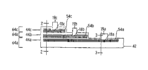
[0025] Figs. la-c illustrate longitudinal cross-sections of an embodiment
of the invention
where the various layers of the distal end 16 of the sensor 12 (shown in Fig.
2), specifically the
sensor layers 64a, 64b, and 64c, are shown. In the illustrated embodiment,
there are three
metallization steps taken to form the electrodes 18a, 18b, and 18c. The
metallization process
forms one or more conductive layers/electrode layers Ma, 54b, and 54c on top
of a base layer
42. The base layer 42 is generally an electrically insulating layer such as a
polyimide substrate,
which may be self-supporting or further supported by another material. In one
embodiment, the
base layer 42 comprises a polyimide tape, dispensed from a reel. Providing the
base layer 42 in
this form can facilitate clean, high density mass production. Further, in some
production
processes using such a polyimide tape, sensors can be produced on both sides
of a tape.
[0026] Fig. 2 illustrates an enlarged fragmented sectional view of a sensor
according to
an embodiment of the invention. The electrodes 18a, 18b, and 18c at the distal
end 16 of the
sensor 12 lead through traces 48a, 48b, and 48c to conductive pads 21a, 21b,
and 21c at a
proximal end 20 of the sensor. Although the figures and the description below
describes the
formation and structure of a sensor with three electrodes, the method and
structure can be used
in a sensor of fewer or more electrodes.
[0027] The first metallization step, shown in Fig. la, applies the
conductive layer 54a
onto the insulative base layer 42. The conductive layer may be provided as a
plurality of thin
film conductive layers, such as an initial chrome-based layer suitable for
chemical adhesion to
the base layer, followed by subsequent formation of a thin film gold-based
layer. Optionally, a
chrome-based top layers may be formed on top of the thin film gold-based
layer. The
conductive layer may also be formed of gold and/or chrome in different ratios
and/or other
adhesive/conductive layers, such as titanium, platinum, tungsten, etc. In
alternative
embodiments, other electrode layer conformations or materials can be used. The
conductive
layer 54a can be applied using electrode deposition, surface sputtering or
another suitable
process step. The electrical circuit of each conductive layer typically
comprises one or more
conductive paths with regions at a proximal end to form contact pads and
regions at a distal end
to form sensor electrodes. Generally, etching is performed to define the
electrical circuit of each
layer. Alternatively, "lift off' may be used, in which the photoresist defines
a pattern prior to
metal sputtering, after which the photoresist is dissolved away (along with
the unwanted metal),
and the metal pattern is left behind. In further embodiments, photoresisting
is performed to
protect the metallized trace and electrode and photoimaging is performed to
cure specified areas.
CA 02622503 2008-03-13
WO 2007/037970 7 PCT/US2006/035382
For example, the conductive layer is covered with a selected photoresist
coating, followed by an
etch step resulting in one or more conductive paths. An electrically
insulative cover layer (or
dielectric layer) 44a, such as a polymer coating, is then applied over at
least portions of the
conductive layer 54a. Acceptable polymer coatings for use as the insulative
cover layer 44a
include, for example, non-toxic biocompatible polymers such as polyimide,
biocompatible
solder masks, epoxy acrylate copolymers, and the like. Further, these coatings
can be
photoimageable to facilitate photolithographic forming of apertures through to
the conductive
layer 54a to expose the electrode 18a. This first metallization step is
finished by developing and
rinsing the produced electrode 18a. In an embodiment this electrode 18a is the
counter
electrode. Alternatively, the electrode 18a may be a working or reference
electrode.
[0028] The second metallization step, shown in Fig. lb, applies a second
conductive
layer 54b over the first insulative cover layer 44a and covering and repeats
the process of
covering the second conductive layer 54b with another insulative cover layer
44b. This
produces another electrode 18b, positioned generally above the first electrode
18a. In an
embodiment, electrode 18b is the working electrode. Alternatively, the
electrode 18b may be a
counter or working electrode. The third metallization step, shown in Fig. lc,
repeats all of the
previous steps to form a third electrode 18c. In an embodiment, electrode 18c
is the reference
electrode. Alternatively, the electrode 18c may be a working or counter
electrode. As shown in
Fig. lc, the electrodes are in a staggered configuration, so that at least a
portion of each electrode
may be exposed. The conductive layers 54a, 54b and 54c, may be directly above
each other or
horizontally displaced from each other (into and out of the page). The
electrodes may further be
configured in any way that allows the electrodes to contact fluid when
inserted into a body of a
patient.
[0029] The sensor 12 is thus shown with the subsequent conductive layers
54a, 54b, and
54c alternating with the insulative layers 44a, 44b, and 44c. In between every
two conductive
layers there is an insulative layer that serves to isolate each conductive
layer so that there is no
trace communication between the layers. Apertures 19a, 19b, and 19c are formed
in the top
insulative cover layer 44c. Although the electrodes 18a, 18b, and 18c are
shown as lying on top
of each other, it is also possible to have them generally above each other,
but spaced sideways so
that they are not directly on top of each other (e.g., horizontally
displaced). This is also true for
the traces that lead to conductive contacts, which electrically connect to the
sensor electronics, at
the opposite end of the sensor from the electrodes. The apertures can be made
through
photolithographic development, laser ablation, chemical milling, etching, or
the like. The
exposed electrodes and/or contact pads can also undergo secondary processing
through the
CA 02622503 2008-03-13
WO 2007/037970 8
PCT/US2006/035382
apertures, such as additional plating processing, to prepare the surfaces,
and/or strengthen the
conductive regions.
[0030] As shown in Fig. 4, typically, a sensor chemistry layer 72 is
disposed on one or
more of the exposed electrodes (e.g., 18a) of the conductive layers. In
certain embodiments, the
sensor chemistry layer 72 is an enzyme layer, for example, glucose oxidase. If
the enzyme layer
is glucose oxidase, it reacts with glucose to produce hydrogen peroxide, which
modulates a
current to the electrode which can be monitored to measure an amount of
glucose present. The
sensor chemistry layer 72 can be applied over portions of the sensor 12 or
over the entire sensor,
including the protective layer (e.g., 44a). The sensor chemistry layer 72 is
generally disposed on
at least portions of a working electrode. In further embodiments, the sensory
chemistry layer
may be disposed on at least portions of other electrodes, such as a counter
electrode. For
example, if the electrode 18a in Fig. 4 is the counter electrode, then the
sensor chemistry layer
72 is disposed on at least portions of the electrode 18a. Example methods for
generating the
sensor chemistry layer include spin coating processes, dip and dry processes,
low shear spraying
processes, ink-jet printing processes, silk screen processes, casting process,
and the like.
[0031] In certain embodiments, the sensor chemistry layer 72 comprises
glucose oxidase
and a carrier protein. The glucose oxidase and carrier protein may be in a
substantially fixed
ratio. In further embodiments, the glucose oxidase and the carrier protein are
distributed in a
substantially uniform manner throughout the disposed enzyme layer. Typically,
the carrier
protein comprises albumin, generally in an amount of about 2-10% by weight,
preferably about
5% by weight. As used herein, "albumin" refers to those albumin proteins
typically used by
artisans to stabilize polypeptide compositions, such as human serum albumin,
bovine serum
albumin, and the like. The application of the glucose oxidase and albumin
mixture may be
made, for example, by a spin coating process, a casting process, a screen
printing process or a
doctor blading process. Optionally, the glucose oxidase layer that is formed
on the sensor is less
than 2 microns in thickness. In further embodiments, the glucose oxidase layer
may be less than
1, 0.5, 0.25 or 0.1 microns in thickness. The choice of the glucose oxidase
layer thickness may
be made to balance fast response and fast hydration verses a sensor lifetime.
Generally, thin
layers hydrate and respond more quickly, but do not last as long. Thick layers
last a long time,
but hydrate more slowly and respond to glucose more slowly.
[0032] The sensor chemistry layer 72 may be coated with one or more cover
layers. In
certain embodiments, as shown in Fig. 4, the cover layer 74 comprises a
membrane that can
regulate the amount of analyte that can contact the enzyme of the sensor
chemistry layer 72. For
example, the cover layer 74 can comprise a glucose limiting membrane, which
regulates the
CA 02622503 2008-03-13
WO 2007/037970 9 PCT/US2006/035382
amount of glucose that contacts the glucose oxidase enzyme layer on an
electrode. Such glucose
limiting membranes can be made from a wide variety of materials suitable for
such purposes,
such as, for example, silicone, polyurethane, cellulose acetate, Nafion,
polyester sulfonic acid
(Kodak AQ), hydrogels, etc. In further embodiments the glucose limiting
membrane includes a
polyamine, such as polyoxypropylene-diamine sold under the trademark JEFFAMINE
, and
polydimethylsiloxane (Structure I) and/or a polysilane, such as
polydimethylsiloxane (PDMS)
(Structure II). In still further embodiments, the glucose limiting membrane is
a random block
copolymer made from JEFFAMINE and PDMS. In further embodiments, the glucose
limiting membrane may also, or alternatively, be a mechanically limiting
membrane. For
example, a glucose limiting membrane may be used that is an oxygen
passing/glucose limiting
polymer, such as silicone, and a small window with the correct ratio size may
be cut into the
polymer to meter glucose directly to the sensor surface.
NH2
0. L+4*=044'
ooey
NF,2
STRUCTURE I
CH3
* ________________
CH3
STRUCTURE II
[0033] In still further embodiments, the JEFFAMINE CD, which is glucose
permeable,
and the PDMS, which is non-glucose permeable but oxygen permeable, are linked
together with
diisocyanide. By using this random block copolymer, an excess of oxygen by the
glucose
oxidase and the electrodes can be ensured along with a restricted amount of
glucose.
[0034] In further embodiments, an adhesion promoter (not shown) is provided
between
the glucose limiting membrane 74 and the sensor chemistry layer 72 to
facilitate contact and/or
adhesion. The adhesion promoter layer can be made from any one of a wide
variety of materials
that facilitates bonding, for example materials comprising a silane compound,
such as an
CA 02622503 2008-03-13
WO 2007/037970
PCT/US2006/035382
aminopropyltriethoxy silane. Alternatively, protein or like molecules in the
sensor chemistry
layer 72 can be sufficiently crosslinked or otherwise prepared to allow the
glucose limiting
membrane 74 to be disposed in direct contact with the sensor chemistry layer
in absence of an
adhesion promoter layer. The adhesion promoter layer can be spin coated,
sprayed, cast, etc.
onto the enzyme layer. It may be exposed to heat and humidity to create
silanol (sticky) groups.
In further embodiments, the layer may be repeated. Although not necessary, the
coating may
help adhesion oxygen buffering. The time for exposure to heat and humidity is
time sufficient to
create silanol (sticky) groups, for example about two hours.
[0035] A hydrophilic membrane 76, which may be non-toxic and biocompatible,
may be
positioned above the glucose limiting membrane 74. The hydrophilic membrane 76
promotes
tolerance of the sensor in the body.
[0036] Typically, the electrodes are formed by one of the variety of
methods known in
the art such as photoresist, etching and rinsing to define the geometry of the
active electrodes.
The electrodes can then be made electrochemically active, for example by
electrodeposition of
platinum black for the working and counter electrode, and silver followed by
silver chloride on
the reference electrode. The sensor chemistry layer is then disposed on the
conductive layer by
a method other than electrochemical deposition, usually followed by vapor
crosslinking, for
example with a dialdehyde, such as glutaraldehyde, or a carbodi-imide.
[0037] The electrodes and conductive layers are generally composed of
conductive
materials. However, they are not limited to conductive elements. Other useful
sensor elements
can be formed from any material that is capable of producing a detectable
signal after interacting
with a preselected analyte whose presence is to be detected. The detectable
signal can be, for
example, an optically detectable change, such as a color change or visible
accumulation of the
desired analyte (e.g., cells). Exemplary such materials include polymers that
bind specific types
of cells, single-strand DNA, antigens, antibodies and reactive fragments
thereof, etc. Sensor
elements can also be formed from materials that are essentially non-reactive
(i.e., controls). The
foregoing alternative sensor elements are beneficially included, for example,
in sensors for use
in cell-sorting assays and assays for the presence of pathogenic organisms,
such as viruses (HIV,
hepatitis-C, etc.), bacteria, protozoa, and the like.
[0038] As shown in Figs. 2 and 3, in one embodiment of the present
invention a sensor
12 has the three electrodes 18a, 18b, and 18c positioned generally one above
the other. The
three electrode layers comprise a plurality of elongated conductive traces
48a, 48b, and 48c
connected to the electrodes 18a, 18b, and 18c on one end and connected to
conductive pads 21a,
21b, and 21c on the opposing proximal segment 20. Each electrode layer is
formed between an
CA 02622503 2008-03-13
WO 2007/037970 11 PCT/US2006/035382
underlying insulative base layer 42 and an overlying insulative cover layer
44. Apertures (not
shown) may be formed on the insulative cover layer 44 to expose the distal
segment 16 and the
proximal segment 20 of the electrodes. In a glucose monitoring application,
the flexible sensor
12 is placed transcutaneously so that the distal segment 16 is in direct
contact with patient blood
or extracellular fluid, and wherein the proximal segment 20 is disposed
externally for convenient
connection, either by wired or wireless communication, to a monitoring device
(not shown).
[0039] One or more sensors are formed on a rigid flat substrate, such as a
glass plate or a
ceramic. When finished, the sensors may be removed from the rigid flat
substrate by a suitable
method, such as laser cutting. Other materials that can be used for the
substrate include, but are
not limited to, stainless steel, aluminum, and plastic materials. As seen in
Fig. 7, the flexible
sensors 12a, 12b, and 12c are formed in a manner which is compatible with
photolithographic
mask and etch techniques, but where the sensors 12a, 12b, and 12c are not
physically adhered or
attached directly to the substrate 52. Each sensor comprises a plurality of
thin film electrodes
18a, 18b, and 18c formed between an underlying insulative base layer 42 and an
insulative cover
layer 44. A plurality of elongated conductive traces 48a, 48b, and 48e may
connect the proximal
segment end 20 to the distal segment end 16. At the proximal segment end 20,
contact pads 21a,
21b, and 21c are formed. Apertures (not shown) formed in the insulative cover
layer expose the
distal end 16 portion of the electrodes 18a, 18b, and 18c so that they are in
direct contact with
patient blood or extracellular fluid.
[0040] In one embodiment of a sensor set, shown in Figs. 5 and 6, a
flexible
electrochemical sensor 12 is constructed according to so-called thin film mask
techniques to
include elongated thin film conductors embedded or encased between layers of a
selected
insulative material such as polyimide film or sheet. The sensor electrodes 18
(shown in
exaggerated form in the drawings) at a tip end of the sensor distal segment 16
are exposed
through one of the insulative layers for direct contact with patient fluids,
such as blood and/or
interstitial fluids, when the sensor is transcutaneously placed. Fig. 6 shows
how the distal
segment 16 is joined to a proximal segment 20, the end of which terminates in
suitable
conductive contact pads or the like which are also exposed through one of the
insulative layers.
As illustrated schematically in Fig. 6, the proximal segment 20 and the
contact pads thereon are
adapted for electrical connection to a suitable monitor 22 for monitoring
patient condition in
response to signals derived from the sensor electrodes 18. The sensor
electronics may be
separated from the sensor by wire or be attached directly on the sensor. For
example, the sensor
may be housed in a sensor device including a housing that contains all of the
sensor electronics,
including any transmitter necessary to transmit data to a monitor or other
device. The sensor
CA 02622503 2013-05-09
WO 2007;037970 12 PCT1JS2006035382
device alternatively may include two portions, one portion housing the sensor
and the other
portion housing the sensor electronics. The sensor electronics portion could
attach to the sensor
portion in a side-to-side or top-to-bottom configuration, or any other
configuration that would
connect the two portions together. If the sensor electronics are in a housing
separated by a wire
from the sensor, the sensor electronics housing may be adapted to be placed
onto the user's skin
or placed on the user's clothing in a convenient manner. The connection to the
monitor 22 may
be wired or wireless. In a wired connection, the sensor electronics may
essentially be included
in the monitor instead of in a housing with the sensor. Alternatively, sensor
electronics may be
included with the sensor as described above. A wire could connect the sensor
electronics to the
monitor. Examples of wireless connection include, but are not limited to,
radio frequency,
infrared, WiFi, ZigBee and Bluetooth. Additional wireless connections further
include single
frequency communication, spread spectrum communication, adaptive frequency
selection and
frequency hopping communication. In further embodiments, some of the
electronics may be
housed on the sensor and other portions may be in a detachable device. For
example, the
electronics that process and digitize the sensor signal may be with the
sensor, while data storage,
telemetry electronics, and any transmission antenna may be housed separately.
Other
distributions of electronics are also possible, and it is further possible to
have duplicates of
electronics in each portion. Additionally, a battery may be in one or both
portion. In further
embodiments, the sensor electronics may include a minimal antenna to allow
transmission of
sensor data over a short distance to a separately located transmitter, which
would transmit the
data over greater distances. For example, the antenna could have a range of up
to 6 inches,
while the transmitter sends the information to the display, which could be
over 10 feet away.
[00411 Further
description of flexible thin film sensors of this general type may be found
in U.S. Pat. No. 5,482,473. The
proximal segment 20
may be conveniently connected electrically to the monitor 22 by means of a
connector block 24
as shown and described in U.S. Pat. No. 5,482,473,
[00421 The
overall sensor height of the sensor 12 (from base to top insulative layer) may
be about 0.001 inches or 25 microns. The base layer is about 12 microns and
each insulative
layer is about 5 microns. The conductive/electrode layers are each in the
range of several
thousand angstroms. Any of these layers could be thicker if desired. The
overall width of the
sensor is as small as about 150 microns. It could be slightly larger, about
250 microns or 0.010
inches. The width could also larger if desired. The length of the sensor is
dependant on how
CA 02622503 2008-03-13
WO 2007/037970 13
PCT/US2006/035382
deep the tissue is at the placement site. For example, for subcutaneous
sensing, the sensor
length may be about 0.50 inches to about 1.5 inches, for example, about 1
inch.
[0043] The sensor 12 is carried by a mounting base 26 adapted for placement
onto the
skin of a patient. As shown, the mounting base 26 comprises an enlarged and
generally
rectangular pad having an underside surface coated with a suitable pressure
sensitive adhesive
layer, with a peel-off paper strip 28 normally provided to cover and protect
the adhesive layer,
until the insertion set 10 is ready for use. As shown in Figs. 5 and 6, the
mounting base
comprises upper and lower layers 30 and 32, with the proximal segment 20 of
the flexible sensor
12 sandwiched between. The proximal sensor segment 20 has a forwardmost end
joined to the
distal segment 16 which is folded angularly to extend downwardly through a
slot 34 formed in
the lower base layer 32.
[0044] The insertion needle 14 is adapted for slide-fit reception through a
needle port 36
formed in the upper base layer 30 and further through the lower slot 34 in the
lower base layer
32. As shown in Fig. 5, the insertion needle 14 has a sharpened tip 38 and an
open slot 40 which
extends longitudinally from the tip 38 at the underside of the needle to a
position at least within
the slot 34 in the lower base layer 32. Above the mounting base 26, the
insertion needle 14 may
have a full round cross sectional shape and is desirably closed at a rear end.
In the preferred
embodiment, the slotted needle 14 has a part-circular cross sectional shape,
with an arcuate
dimension or span greater than 180 degrees, such as on arcuate dimension of
about 210 degrees.
This leaves a longitudinal slot in the needle with an arcuate dimension of
about 150 degrees.
[0045] The cannula 15 is shown in Fig. 6 and comprises a part circular
cross section
fitted within the insertion needle 14 to extend downwardly from the mounting
base 26. This
cannula 15 is constructed from a suitable medical grade plastic or elastomer,
such as
polytetrafluoroethylene, silicone, or the like. The cannula 15 has one end
fitted into the slot 34
formed in the lower layer 32 of the mounting base 26, wherein the cannula 15
is desirably
secured to the mounting base by a suitable adhesive or other selected
attachment means. From
the mounting base 26, the cannula extends angularly downwardly with its first
portion nested
within the insertion needle 14, terminating slightly before the needle tip 38.
One or more
apertures 19 are formed in the cannula 15 near the distal segment end 16, in
general alignment
with the sensor electrodes 18, to permit direct electrode exposure to patient
body fluid when the
sensor is transcutaneously placed.
[0046] In use, the insertion set 10 permits quick and easy transcutaneous
placement of
the sensor distal segment 16 at a selected site within the body of the
patient. More specifically,
the peel-off strip 28 is removed from the mounting base 26, at which time the
mounting base 26
CA 02622503 2008-03-13
WO 2007/037970 14
PCT/US2006/035382
can be pressed onto and seated upon the patient's skin. During this step, the
insertion needle 14
pierces the patient's skin and carries the protective cannula 15 with the
sensor distal segment 16
therein to the appropriate transcutaneous placement site. During insertion,
the cannula 15
provides a stable support and guide structure to carry the flexible sensor to
the desired insertion
site.
[0047] When the sensor 12 is transcutaneously placed, with the mounting
base 26 seated
upon the patient's skin, the insertion needle 14 can be slidably withdrawn
from the patient. The
slotted needle geometry permits the insertion needle 14 to slide over and
longitudinally separate
from the second portion of the cannula 15, thereby leaving the cannula 15 as
well as the sensor
distal segment 16 with electrodes 18 at the selected insertion site. These
electrodes 18 are
directly exposed to patient body fluid via the apertures 19. The sensor
proximal segment 20 is
appropriately coupled to the monitor 22, so that the sensor 12 can then be
used over a prolonged
period of time for taking blood chemistry readings, such as BG readings in a
diabetic patient. In
an embodiment, when the insertion needle is withdrawn, a protective sheath
(not shown)
contained in the mounting base is dislodged and covers the needle tip as the
needle is separated
from the mounting base. If desired, the cannula 15 can also be used to deliver
medication and/or
sensor calibration fluid to the vicinity of the electrodes 18, or alternately
to withdraw patient
fluid such as blood for analysis.
[0048] While the description above refers to particular embodiments of the
present
invention, it will be understood that many modifications may be made without
departing from
the spirit thereof. The accompanying claims are intended to cover such
modifications as would
fall within the true scope and spirit of the present invention.
[0049] The presently disclosed embodiments are, therefore, to be
considered in all
respects as illustrative and not restrictive, the scope of the invention being
indicated by the
appended claims rather than the foregoing description. All changes that come
within the
meaning of and range of equivalency of the claims are intended to be embraced
therein.
EXAMPLES
[0050] The examples set forth below are illustrative of different
compositions and
conditions that can be used in practicing the invention. All proportions are
by weight unless
otherwise indicated. It will be apparent, however, that the invention can be
practiced with many
types of compositions and can have many different uses in accordance with the
disclosure above
and as pointed out hereinafter.
CA 02622503 2008-03-13
WO 2007/037970 15 PCT/US2006/035382
Example I
Step 1: Counter Electrode Metallization Sten
[0051] A KAPTON Opolyimide base is used as a base layer and spin coated on
a rigid
substrate, such as glass. The first metallization comprised sputter-based
chrome, gold and top-
chrome. The top chrome pattern was photoresisted using photomask to protect
the metallized
trace and counter electrode. The uncovered areas of the base-chrome and gold
were etched. The
etching was performed at 50 C for the gold and at ambient temperature for the
chrome. The
strip photoresisting was performed in isopropyl alcohol ("WA") at ambient
temperature, and
then again on all areas except the counter electrode, bond pad, and plating
pad, at ambient
temperature. A second etching was then performed on the top-chrome of all
uncovered areas at
ambient temperature. Strip photoresisting was performed again in IPA at
ambient temperature.
Polyimide was spin coated on as an insulative layer. Photoimaging was then
performed to cure
specific areas. The resulting electrode layer was developed and rinsed.
Step 2: Working Electrode Metallization Step
[0052] _ The next electrode layer is formed generally above the counter
electrode layer.
This second metallization step involves the same sputter base-chrome and gold
as a base layer.
Photoresisting is performed using photomask to protect the working metallized
trace and
working electrode being formed. Etch is performed on the uncovered areas at 50
C for the gold
and at ambient temperature for the chrome. Strip photoresisting is again
performed in IPA at
ambient temperature. Next, photoresisting is performed on all areas except the
counter
electrode, bond pad, and plating pad. Etching is performed on all uncovered
areas of the top-
chrome at ambient temperature. Strip photoresisting is performed in IPA at
ambient
temperature. Polyimide was spin coated on as an insulative layer. Photoimaging
was then
performed to cure specific areas. The resulting electrode layer was developed
and rinsed.
Step 3: Reference Electrode Metallization Step
[0053] The next electrode layer is formed generally above the counter
electrode layer.
This third metallization step also involves the sputter base-chrome and gold
combination as a
base layer. Photoresisting is performed using photomask to protect the working
metallized trace
and working electrode being formed. Etch is performed on the uncovered areas
at 50 C for the
gold and at ambient temperature for the chrome. Strip photoresisting is again
performed in IPA
at ambient temperature. Next, photoresisting is performed on all areas except
the counter
electrode, bond pad, and plating pad. Etching is performed on all uncovered
areas of the top-
CA 02622503 2008-03-13
WO 2007/037970 16
PCT/US2006/035382
chrome at ambient temperature. Strip photoresisting is performed in IPA at
ambient
temperature. Polyimide was spin coated on as an insulative layer. Photoimaging
was then
performed to cure specific areas. The resulting electrode layer was developed
and rinsed. After
all three electrode layers are formed, the layers are subjected to a final
bake at a high
temperature, such as 325 C.