Note: Descriptions are shown in the official language in which they were submitted.
CA 02623061 2008-02-29
ZERO CROSSING CIRCUIT
Cross Reference to Related Application
This application claims priority from United States Provisional Patent
Application No. US Provisional Application No. 60/904,387 filed March 2, 2007
entitled
Zero-Crossing Detector.
Field of the Invention
The invention relates to the field of devices for detecting a zero-crossing
voltage of an alternating current signal, and in particular to such a device
wherein a delay
inducing circuit element causes a trigger signal upon the voltage dropping to
a predetermined
level thereby signalling the zero crossing as the voltage coincides with the
actual zero
crossing.
Background of the Invention
Zero crossing is a commonly used term in electronics. In alternating current,
the
zero crossing is the instantaneous point at which there is no voltage present.
This occurs twice
during each cycle. Zero crossing detectors are used to detect the zero cross
in solid state
relays. The purpose of the circuit is to turn on the solid state relay as
close to the zero crossing
as possible. Zero crossing detectors are also used in systems to coordinate
operation. Devices
plugged into the AC power can keep track of the zero crossing to perform
various timing
dependant operations as each device sees the same AC power. For these and
other reasons zero
cross detector circuits have important applications.
Nakata et al. in United States Patent No. 6,664,817 which issued December 16,
2003, entitled Zero-Cross Detection Circuit discloses a power supply device
including a fall-
wave rectifying and smoothing circuit powered from a commercial AC power
supply via two
I
CA 02623061 2008-02-29
power supply lines, a switching regulator for separating and stepping down the
output from the
full-wave rectifying and smoothing circuit to output a desired DC voltage, and
two ca.pacitors
after the full-wave rectifying and smoothing circuit for the terminal noise
suppression purpose,
a zero-cross detection circuit includes a transistor of which the emitter is
connected to the low-
voltage output terminal of the full-wave rectifying and smoothing circuit for
outputting a zero-
cross detection signal from the collector; a first resistor is connected
between the base and
emitter of the transistor; a second resistor is connected between one of the
power supply lines
and the base of the transistor; and a third resistor is connected between the
other power supply
line and the emitter of the transistor.
Gottshall et al. in United States Patent No. 5,606,273 which issued February
25,
1997, entitled Zero Crossing Detector Circuit discloses in one aspect a zero
crossing detecting
circuit. The circuit includes a first comparator having an inverting and non-
inverting input
connected to an input signal. The non-inverting input of the first comparator
is further
connected to the first comparator output to provide a feed forward path. A
second comparator
is additionally included having an output connected to the first comparator
inverting input.
This provides the inverting input of the first comparator with a reference
voltage that is
substantially equal to that of the first comparator non-inverting input;
thereby, providing the
first comparator with balanced inputs.
Floelanan in United States Patent No. 5,239,209 which issued August 24, 1993,
entitled Zero Crossing Detection Circuit discloses a zero crossing detection
circuit whieh
produces an output signal which changes state to indicate the occurrence of a
positive-going
zero crossing of an AC input signal. The circuit includes first and second
input terminals, a
current sensitive switch such as an opto-isolator, first and second current
regulators, and a
voltage limiter. The first current regulator is connected in series with the
current sensitive
switch, and the voltage limiter is connected in parallel with the first
current regulator and the
current sensitive switch. The second current regulator is connected between
the first input
terminal and the parallel combination of the voltage limiter and the first
current regulator and
the current sensitive switch. The first current regulator limits current
through the current
2
CA 02623061 2008-02-29
sensitive switch to a first current limit level, and the second current
regulator limits current
flowing between the first and second input terminals to a second current limit
level which is
greater than the first current level. The zero crossing detection circuit
offers the ability to sense
zero crossings of AC input signals having a wide range of AC voltages.
Summary of the Invention
In summary, the improved zero crossing circuit according to one aspect of the
present invention may be characterized as a circuit for detecting a zero-
crossing voltage in an
alternating current signal wherein the circuit may include a signal outputting
means for
registering a sharp-edged definitive signal having a magnitude sufficient to
be readily
detectable, and an isolation means cooperating with the signal outputting
means, and wherein
the improvement includes a delay-inducing means cooperating with the signal
outputting
means for applying a substantially constant time delay to the signal. In
particular, the delay-
inducing means includes a switch circuit and a delay circuit. The switch
circuit commences
the time delay by the delay circuit upon a triggering voltage being reached.
Tlie time delay
circuit is adapted so that the time delay equates to a time period required
for the triggering
voltage to change to zero so as to cross zero voltage substantially as the
time delay expires.
In one embodiment the switch circuit includes at least one transistor and the
delay circuit includes at least one capacitor, and wherein the at least one
transistor and the at
least one capacitor are mounted in parallel between a line voltage and a
neutral line. The at
least one transistor may be single transistor, and the at least one capacitor
may be a single
capacitor. At least one resistor may be advantageously mounted in series with
a corresponding
at least one transistor. The signal outputting means may be a thysistor, or
other avalanche
means, and the isolation means may be an opto-coupler.
In the above circuit a method according to another aspect of the present
invention for detecting a zero-crossing voltage in an alteraating current
signal includes the
steps o~
3
CA 02623061 2008-02-29
(a) adapting the switch circuit to cooperate with the delay circuit so as to
commence the time delay upon the voltage reaching the triggering
voltage and so as to tliereby delay a sharp-edged definitive signal by the
time delay,
(b) commencing the time delay upon the voltage reaching the triggering
voltage,
(c) delaying the signal by the time delay,
(d) adapting the time delay so that it is substantially constant and expires
at
a time substantially equating to when the voltage crosses a zero voltage
in the alternating current signal,
(e) generating the signal after the time delay and substantially
simultaneously with the voltage crossing the zero voltage.
Brief Descniption of the Drawinas
With reference to the drawings wherein similar characters of reference denote
corresponding parts in each view:
Figure 1 illustrates, in a first trace, the sinusoidal rise and fall of a
voltage in an
alternating current, and in.a second. trace the output of a device registering
the zero crossing of
the voltage.
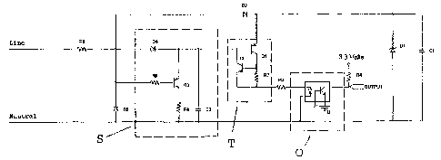
Figure 2a is a prior art circuit containing a thyristor-like trigger and an
optocoupler.
Figure 2b is a prior art variant of the circuit ofFigure 2a.
Figure 2c is a prior art variant of the circuit of Figure 2a showing the
optocoupler removed.
4
CA 02623061 2008-02-29
Figure 3 is a trace of the sinusoidal rise and fall of voltage in an
alternating
current illustrating a brief, downward voltage spike momentarily pulling down
the voltage
trace from approximately positive 50 volts to negative 50 volts prior to the
sinusoidal voltage
trace dropping to its zero crossing.
Figure 4 is, in a first trace, the voltage trace of Figure 3, and its second
trace,
the output of a device for detecting zero crossings showing zero crossings
registering due to
both the downward voltage spike and the actual zero crossing of the sinusoidal
voltage trace.
Figure 5 is a prior art circuit illustrating the use of a capacitor C2 before
the
trigger element T.
Figure 6 is a circuit according to one embodiment of the present invention
showing within circuit element S one embodiment of the delay-inducing means
according to
the present invention. Figure 6a is a sinusoidal voltage trace
diagrammatically illustrating the time
delay D resultant of the operation. of circuit element S in Figure 6.
Figure 7 illustrates, in a first trace, a voltage trace similar to that of
Figure 3
including a similar voltage spike, and in a second trace, illustrates the
output of a device for
detecting zero crossings which, employing the present invention, shows an
output registering
only the actual zero crossing of the sinusoidal voltage trace.
Figure 8 is a further embodiment of the improved circuit according to the
present invention, being a variant of the circuit of Figure 6.
Figure 9 is a further variant of the circuit of Figure 6 showing the
optocoupler
removed.
5
CA 02623061 2008-02-29
Detailed Description of Embodiiments of the Invention
Many systems take advantage of AC line voltage to help synchronize
transmissions of data and other timing details. An example would be a number
of small RF
devices that are all being powered from the AC line and wish to synchronize
their
transmissions to avoid transmission collisions. An effective method for
monitoring the AC line
is to use a zero crossing detector. The zero crossing detector triggers when
the line voltage
transitions from positive to negative (or vise versa) with respect to
neutra.i. Figure 1 shows
this.
The first trace 10 of Figure 1 is the line to neutral voltage scaled by
dividing it
by 40. The second trace 12 shows the output of the zero crossing circuit shown
in Figure 2a.
As can be seen the output 24 pulses low at the negative-going zero crossing of
the line voltage.
The 3.3 volts of the second trace 12 comes from a power supply that powers a
microprocessor
or the equivalent.
The circuits of Figure 2a work as follows: Assuming that the line voltage is
lower than neutral and capacitor Cl is discharged a small amount of current
flows though
diode D3 and resistor R1. As used herein, the letters C, D, R and Q refer to
capacitors, diodes,
resistors and transistors respectively. When the line voltage becomes positive
current starts to
flow through RI and D2 and begins charging Cl. Zener diode DI elamps the
voltage across
Cl, VC1, at a reasonable level. When the line voltage drops below VC1 diode D2
becomes
reverse biased and VC1 stays essentially constant for the brief period before
the circuit
triggers. When the line voltage falls sufficiently below VCI for transistor Q1
to start
conduction the triggered element T is triggered. Q1 and Q2 form the functional
equivalent of
a tliyristor or SCR or other avalanche-type device as is well known in the
art. When triggered
element T is triggered, current flows from C1 through T, R3 and the light
emitting diode in the
optocoupler O. This causes the optotransistor in optocoupler 0 to conduct
thereby pulling the
output low. The output in this figure is normally pulled high by resistor R4
and a 3.3 Volt
6
CA 02623061 2008-02-29
supply. As will be understood by those skilled in the art the voltage need not
be 3.3 Volts as
indicated. As well optocoupler 0 could be used to pull the output high briefly
and could be a
different form of optocoupler, etc. It is also possible to use a pulse
transformer in place of an
optical isolation means such as an optocoupler. The circuit element symbolized
by optocoupler
0 is meant to include other means of isolation and is thus not intended to be
limiting. Resistor
R2 reduces the sensitivity of triggered element T and may or may not be
present. Resistor R3
is used to limit the current flowing from Cl.
Figure 2b shows a variation of the circuit of Figure 2a, wherein R3 is placed
before the trigger element T and R2 is absent.
As mentioned above the voltage of 3.3 Volts need not be used and the
optocoupler need not be the same or used in the same way as indicated in
Figures 2a and 2b.
In fact the circuit can be used in a non-isolated manner where the output is
taken directly off
R3 as shown in Figure 2c. Here the output will pulse high when triggered
element T is
triggered.
The problem with the circuit of Figures 2a - 2c is that the circuit is
susceptible
to false triggering due to line noise, especially voltage spikes. Since the
entire purpose of the
circuit is to trigger a shaip definitive detectable output such as output 24,
especially at the
leading edge of the output at the zero crossing, false triggering is to be
avoided. Figure 3
shows line to neutral voltage 14 with a voltage spike 16 scaled by dividing it
by 40. Figure 4
shows in the second trace 18 the output of the circuit of Figure 2a false
triggering output 20
which is not at the zero crossing 22 due to the voltage spike 16 of Figure 3.
It is possible and known to filter voltage spikes with the addition of some
capacitance C2 after resistor RI of Figure 2. Figure 5 shows this. This is not
an optimal
solution however because for C2 to be effective at preventing false triggering
it will cause a
time lag that makes the circuit trigger significantly later than the zero
crossing. As well, this
time lag is sensitive to temperature. That is, the circuit's output moves
substantially with
7
CA 02623061 2008-02-29
respect to the zero crossing as its operating temperature changes. This makes
the time lag
variable and thus difficult to compensate for in software and not as useful
for timing of
devices, data, etc.
Figure 6 shows an improved circuit according to one embodiment of the present
invention wherein diode D4, resistors R5, R6 and transistor Q3 have been added
to the circuit
of Figure 5. These components in combination with capacitor C2 form in essence
a switch,
shown for ease of identification within a box S, that, in cooperation with the
rest of the circuit,
bas a substantially constant time delay D, as shown diagrammatically in Figure
6a, that
prevents the voltage spikes from causing false triggering. That is, if the
switch is turned on for
a brief time and then turned off, as would happen in the case of a voltage
spike 16 such as
shown in Figure 3, the circuit does not trigger a false output 20 such as seen
in Figure 4.
Rather, the false output 20 on the second trace 18 is avoided so long as the
spike 16 is short enough in duration that is the spike is not seen as it has a
duration less than
the substantially constant time delay D. As seen in Figure 6a, time delay D
corresponds to the
time it takes the voltage of the power line to fall by the amount of VC1. By
way of example,
not intended to be limiting, a realistic voltage spike 16 may have a duration
in the order of 10
microseconds, so a time delay provided by the switch elements of the circuit
in the order of at
least slightly greater than 10 microseconds, or some multiple thereof (10 - 30
microseconds
for example), would. be advantageous. The values of the components can be
chosen so that
during a true zero crossing the circuit produces an output without a time lag.
As well the
circuit of Figure 6 is much less temperature sensitive than the circuit shown
in Figure 5.
Figure 7 shows the output of the improved circuit of Figure 6 with the same
voltage spike 16 as shown in Figures 3 and 4. As can be seen the circuit does
not falsely
trigger, and it produces an output 24 at the zero crossing 22. As may be seen,
advantageously
output 24 is a sharp-edged definitive signal having a magnitude sufficient to
be readily
detectable, such as would be produced by a thyristor-like device such as in
triggered element
T. In fact this circuit will not falsely trigger even for much larger voltage
spikes.
8
CA 02623061 2008-02-29
Figure 8 shows a fiuther elnbodiment of the improved circuit according to the
present invention, which is a variation of the circuit of Figure 6. Figure 9
shows a non-isolated
version of the improved circuit on Figure 6.
By way of example, not intending to be limiting, the components inside box S
of figure 6 may have the following values/descriptions.
R5 470 kiloOhms
R6 39 kiloOhzns
C2 30 nanoFarads
D4 1N4148
Q3 2N3906
These components would cooperate with D I and Cl to produce an output
substantially at the zero crossing for 120 VAC for D1, Cl having the following
values/descriptions:
Dl BZXC10 (10 Volt Zener diode)
Cl 30 nanoFarads
Although the previous discussion has focused on the synchronization of
systems, the circuit has other uses. Often zero cross detectors are used to
switch. loads at the
zero crossing so as to minimize the in-rush of current to a load and/or
inductive kicks from a
load. Since the improved eircuit of the present invention will not false
trigger and will trigger
at the zero cross it has applications for these devices as well.
As will be apparent to those slQlled in the art in the light of the foregoing
disclosure, many alterations and modifications are possible in the practice of
this invention
9
CA 02623061 2008-02-29
without departing from the spirit or scope thereof. Accordingly, the scope of
the invention is
to be construed in accordance with the substance defined by the following
clairns.
I0