Note: Descriptions are shown in the official language in which they were submitted.
CA 02623767 2008-02-29
Stepless Dimming Fluorescent Lamp and Ballast Thereof
TECHNICAL FIELD
The present invention relates to a fluorescent lamp ballast capable of
stepless
dimming, and more particularly to a fluorescent lamp ballast adapted for
enabling a
fluorescent lamp and particularly a compact fluorescent lamp to effect dimming
steplessly with a regular silicon controlled rectifier dimmer.
BACKGROUND OF THE INVENTION
A dimmable fluorescent lamp is desired by the public for a long time. Unlike
an
incandescence lamp which can effect dimming with a common silicon controlled
rectifier (SCR) dimmer, a fluorescent lamp is a nonlinear load and exhibits a
negative resistance characteristic such that it cannot effect dimming with the
regular
SCR dimmer. In the available domestic and commercial dimmers a TRIAC is
usually employed, and a characteristic of which is the requirement of a
holding
current for maintaining the on state thereof after it has been triggered. The
characteristic suits the operation modes of a resistive load such as an
incandescence
lamp so well but being undesired by a capacitive load such as a fluorescent
lamp, for
the reason that blinking might occur owing to the discontinuity and
instability in
course of dimming operation while such dimmers are employed, which in turns
has
an adverse effect on the illumination effect and the life span of the
fluorescent lamp.
In this way, the incandescence lamp having high power consumption and short
lifespan is the only choice for those who want to use a dimmer to enjoy
dimming
function and effect.
-1-
CA 02623767 2008-02-29
SUMMARY OF THE INVENTION
An object of the present invention is to provide a novel fluorescent lamp
ballast
adapted for use with a SCR dimmer, and a fluorescent lamp and particularly a
compact fluorescent lamp making use of the ballast, which is capable of
effecting
stepless dimming and providing a stable dimming effect.
Accordingly, a fluorescent lamp adapted for effecting stepless dimming with a
regular silicon controlled rectifier dimmer is provided by the present
invention,
which comprises:
a filter and rectifier circuit;
a DC high voltage stabilizing circuit coupled with the filter and rectifier
circuit;
a voltage signal detection and frequency control circuit coupled with the DC
high voltage stabilizing circuit;
a lamp load coupled with the voltage signal detection and frequency control
circuit; and
a lamp current feedback circuit coupled between the lamp load and the voltage
signal detection and frequency control circuit;
characterized in that it further comprises a voltage signal sampling circuit
coupled between the filter and rectifier circuit and the voltage signal
detection and
frequency control circuit, which is configured to detect and convert a
variation in
conduction angle of the SCR dimmer, so as to correspondingly change output of
the
voltage signal detection and frequency control circuit or working current and
power
-2-
CA 02623767 2008-02-29
factor of the lamp load.
According to an embodiment of the present invention, the voltage signal
sampling
circuit comprises
a plurality of first resistors in series connection, wherein one of the
plurality of
first resistors is respectively connected in parallel with
a first capacitor,
a first zener diode and a second resistor in series connection,
a first diode and a third resistor in series connection,
a second zener diode,
a fourth resistor and a second capacitor in series connection; and
a fifth resistor having its one end coupled with a junction point between the
fourth resistor and the second capacitor; wherein the second capacitor is
configured
to provide a output voltage for the voltage signal sampling circuit.
According to an embodiment of the present invention, the DC high voltage
stabilizing circuit comprises two serially connected diodes and a capacitor
having its
one end coupled with a junction point between the two serially connected
diodes.
According to another embodiment of the present invention, the voltage signal
detection and frequency control circuit comprises an integrated circuit block
and
various peripheral devices coupled correspondingly at respective pins of the
integrated circuit block. Preferably, the integrated circuit block comprises a
program
by which output signal frequency of the integrated circuit block is altered
correspondingly in response to a voltage value at a voltage signal detection
pin of
the integrated circuit block, thereby changing linearly the working frequency
and
-3-
CA 02623767 2008-02-29
luminous intensity of the lamp load. To be specific, the voltage signal
sampling
circuit provides a voltage variation signal generated by the SCR dimmer to the
voltage signal detection pin of the integrated circuit block U1, and then the
integrated circuit block U1 change correspondingly its output oscillation
frequency
in response to the level of voltage at the voltage signal detection pin,
whereby
changing the output power factor to regulate the output of the lamp load of
the
fluorescent lamp. According to the present invention, when the conduction
angle of
the SCR dimmer is changed from the maximum value to a specific value and then
back to the maximum value from the specific value, it will be regarded as an
operation cycle during which the lamp load will be correspondingly migrated
from a
working state of highest luminous intensity to a working state of relatively
low
luminous intensity and then back to the working state of the highest luminous
intensity in a linear manner, whereby a linear stepless dimming of the
fluorescent
lamp is realized.
A fluorescent lamp according to the present invention can be adapted widely to
replace the incandescence lamp having relative high power consumption and
short
lifespan in various locations where a SCR dimmer is installed for dimming
effect,
and which is more economical and favourable for enviromnental conservation as
it
employs only those electronic elements being compact in size and low in power
consumption.
BRIEF DESCRIPTION OF THE DRAWINGS
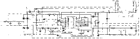
Figure 1 is a circuit diagram of a fluorescent lamp capable of effecting
stepless
-4-
CA 02623767 2008-02-29
dimming with a regular silicon controlled rectifier dimmer and the ballast
thereof.
DETAILED DESCRIPTION OF THE PREFERRED EMBODIMENTS
Referring to Figure 1, a fluorescent lamp capable of effecting stepless
dimming with
a regular silicon controlled rectifier dimmer in accordance with the present
invention
is illustrated, which comprises a filter and rectifier circuit 1, a DC high
voltage
stabilizing circuit 2, a voltage signal sampling circuit 3, a lamp load 4, a
lamp
current feedback circuit 5, and a voltage signal detection and frequency
control
circuit 6.
According to the embodiment, the filter and rectifier circuit 1 comprises a71
filter
circuit whereby filtering high frequency interference waves from coupled AC
power
source and converting AC input voltage into DC voltage.
The output end of the filter and rectifier circuit 1 couples with the input
end of the
DC high voltage stabilizing circuit 2 having its output end connected to the
voltage
signal detection and frequency control circuit 6 for supplying a stable DC
high
voltage to the integrated circuit block U1 of the voltage signal detection and
frequency control circuit 6 thereof. The feedback end of the DC high voltage
stabilizing circuit 2 is connected to the output end of the voltage signal
detection and
frequency control circuit 6 whereby feeding back the high frequency energy
output
thereof into a energy storage capacitor C3 of the DC high voltage stabilizing
circuit
2. The DC high voltage stabilizing circuit 2 comprises two serially connected
diodes
D1, D2 and a capacitor C24 having its one end coupled with a junction point
between the two serially connected diodes D1, D2 and its another end coupled
with
-5-
CA 02623767 2008-02-29
a capacitor C20 of the voltage signal detection and frequency control circuit
6
whereby to receive high frequency energy from a junction point in between the
lamp
load 4 and the capacitor C20, and the high frequency energy is fed into the
energy
storage capacitor C3 after being rectified by the diode D2.
The voltage signal sampling circuit 3 converts a variation in conduction phase
angle
of the SCR dimmer into a voltage signal and delivers such signal to a voltage
detection pin CS+ of an integrated circuit block U1. The voltage signal
sampling
circuit 3 might comprise a plurality of resistors R2, R3, R4, R6, R7, R11,
R16,
capacitors C4, C9, a diode D6 and two zener diodes Z1, Z3; as shown in the
figure,
the input end of which couples with the output end of the filter and rectifier
circuit I
while its output end being connected to the voltage detection pin (pin 8) CS+
of the
integrated circuit block U1. The voltage at the output end of the filter and
rectifier
circuit 1 is stepped down via resistors R2, R7, and then it is divided through
the
resistor R3 and charges up the capacitor C4. A required phase angle signal for
dimming can be sampled at capacitor C9 after the divided voltage pass through
and
being processed by C4, Z1, R4, D6, R6, Z3, R11, and R16; and the signal is
then
delivered to the voltage detection pin CS+ of the integrated circuit block U1.
As can be seen, the lamp current feedback circuit 5 comprises resistors R15,
R19, a
capacitor C27 and two diodes D3, D4.
The voltage signal detection and frequency control circuit 6 comprises the
integrated
circuit block U 1 capable of controlling the working frequency and generating
high
frequency signals, and its associated peripheral devices, which consist of
resistors,
capacitors, diodes and zener diodes, being connected according to the
requirements
-6-
CA 02623767 2008-02-29
on the connection of the pins as stated in the specification of the integrated
circuit
block. The integrated circuit block Ul comprises the voltage signal detection
pin
CS+ coupled with the output end of the voltage signal sampling circuit 3,
whereby
the integrated circuit block U1 can change linearly the frequency of its
output signal
after a valid dimming phase angle signal is detected. After oscillation, the
output
signal enables the stable operation of the lamp load 4. In this way, when the
frequency of output signal of the integrated circuit block U1 is altered, the
working
frequency and the luminous intensity of the lamp load 4 will be changed
whereby
the dimming operation is realized.
The voltage signal sampling circuit 3 and the voltage signal detection and
frequency
control circuit 6 according to the present invention make use of the inverse
proportional relationship between the effective value of the DC pulse voltage
obtained at sampling point and the conduction phase angle of the SCR dimmer,
which means the output voltage of the voltage signal sampling circuit 3 will
be
correspondingly decreased / increased when the phase angle is increased /
decreased.
In this way, the working current or frequency of the lamp load 5 can be
linearly
altered to effect stepless dimming while the output frequency of U1 is
increased /
decreased along with the decrease / increase of the voltage at the voltage
signal
detection pin of the integrated circuit block U1.
Further, the DC high voltage stabilizing circuit 2 is employed to feed back
the high
frequency electric energy generated by the voltage signal detection and
frequency
control circuit 6 into the energy storage capacitor C3 for ensuring the DC
high
voltage will not drop dramatically during the frequency modulation of a
specific
range, thereby enabling the lamp load 4 to be operated in a more reliable and
stable
-7-
CA 02623767 2008-02-29
manner.
The foregoing voltage signal sampling circuit 3 and the voltage signal
detection and
frequency control circuit 6 as shown are designed specifically for effecting
the
stepless dimming of the fluorescent lamps, they might be complementary to each
other or cooperate with other corresponding and functionally equivalent
circuits
such that a stable, linear and flicker-free stepless dimming can be effected
with a
SCR dimmer by setting an appropriate program and parameters thereof.
The voltage signal detection and frequency control circuit 6 of the present
invention
identifies mainly the conduction phase angles of the SCR dimmer and generates
corresponding dimming control signals by making use of the integrated circuit
block
U1, thereby it is simple in configuration, stable in dimming performance and
particularly adapted for use in a compact fluorescent lamp.
It should be understood that the above embodiment is merely an exemplary but
not
limitative example, while any other technical solutions obtained through
logical
analysis, deduction or limited experiments made by a person skilled in the art
in
accordance with the conception and teachings set forth hereinbefore shall all
fall
within the scope of the following claims of the present invention.
-8-