Note: Descriptions are shown in the official language in which they were submitted.
CA 02624262 2008-03-28
WO 2007/041551 PCT/US2006/038565
3D MINIATURE PRECONCENTRATOR AND INLET SAMPLE HEATER
FIELD OF THE INVENTION
[0001] The present invention relates to a preconcentrator and inlet sample
heater for an
analytical instrument. More particularly, the present invention relates to a
micro-machined
preconcentrator and inlet sample heater with a three-dimensional structure,
integral heating, and a
semiconductor substrate.
BACKGROUND OF THE INVENTION
[0002] In analytical chemistry, preconcentrators have been used for many years
to collect
molecules that are present in low concentrations. Analytical instruments may
not be able to
detect molecules in such low concentrations. Preconcentrators accumulate and
concentrate one
or more chemical species of interest over time, so that the analytical
instruments can detect the
molecule. Thus, preconcentrators increase the sensitivity of analytical
techniques such as, e.g.,
gas chromatography, mass spectrometry, and ion mobility spectrometry (IMS).
[0003] Preconcentrators are particularly useful to aid in the detection of
trace compounds such
as drugs, explosives, and other toxic agents. As these compounds are typically
found in the field,
battery-powered portable detectors have been developed.
[0004] The key feature of a preconcentrator is the ability to adsorb an
analyte and then release
it at a specific temperature. To adsorb the analyte, special materials called
adsorbent-resins have
been developed. Adsorbent resins are typically high surface area powders and
the nature of the
analyte determines the choice of resin.
[0005] Existing preconcentrators usually consist of an adsorbent 'slug' inside
a tube. The
sample passes through the tube and analytes adsorb onto the slug. When enough
analyte has
accumulated, the slug is heated to release a concentrated 'plume' of analyte
into the detector for
techniques such as e.g. IMS. These preconcentrators have a low surface area to
volume ratio,
requiring a long time to accumulate a sufficient quantity of analyte.
Furthermore, due to a
pressure drop across the preconcentrator, inline use with existing detectors
may require changing
the internal air handling. Such changes can be difficult, expensive and even
preclude retrofitting
of preconcentrators to an existing device. The slug is also large requiring a
fair amount of time
and energy to release the analyte. This energy consumption poses a particular
problem when
preconcentrators are used in portable detection systems as it lowers the
battery life.
CA 02624262 2008-03-28
WO 2007/041551 PCT/US2006/038565
[UUU61 For portable systems, micro-machined preconcentrators have been
designed. Typical
inline micro-machined-preconcentrators consist of a thin film serpentine
structure with an
adsorbent coating on top. The structure can have thiclcness in the order of
microns and
consequently is quite fragile. The heating element is external to the device,
limiting thermal
efficiency. A brealc in the structure, which also serves as the heating track,
will ordinarily cause
complete failure.
[0007] The surface area of such concentrators is essentially the surface area
of the top of the
structure, as the thickness is negligible. As a result, such devices have a
relative low surface area
to which the analyte adsorbs. Furthermore, because of their low surface area
it takes a longer
time to preconcentrate the analyte. Once sufficient analyte has accumulated,
current is passed
through the structure and causes desorption. Since the heating of the
preconcentrator is often not
uniform, additional time and energy are required to desorb the analyte.
Furthermore, due to the
non-uniform heating, it is difficult to accurately control desorption of the
analyte.
[0008] Micro-machined preconcentrators may be mounted inline to the detector
or externally.
In an external preconcentrator, the preconcentrator located inside a chamber
and the analyte
enters through an inlet port and leaves through an outlet port. Such
preconcentrators are
disadvantageous in that they add complexity to the apparatus and thus hinder
further
miniaturization.
[0009] U.S. Patent No. 6,239,428 to Kant discloses systems and methods of ion
mobility
spectrometry. The system may contain a preconcentrator whose temperature is
modulated
between two temperatures. The preconcentrator has permeable organic membranes
or thin metal
foils. Consequently, the preconcentrator has low surface area and is quite
fragile.
[0010] U.S. Patent No. 6,171,378 to Manginelli et al. is illustrative of a
micro-machined
external preconcentrator. The preconcentrator contains a substrate with a
suspended membrane,
which serves to support two resistive heating elements on top of which an
adsorbent coating is
deposited. Again, this preconcentrator does not maximize the surface area.
[0011] During the manufacture of a micro-machined preconcentrator,
preconcentration material
is placed on the device. One way to deposit the preconcentration material is
to use ink jet
deposition. This process employs about 70,000 individual drops and is slow and
serial. Ink jet
deposition lacks resolution to create ultra-small geometries and when complex
features have to
be printed, it can be prohibitively expensive.
[0012] There remains a need for a preconcentrator that does not create a large
pressure drop,
requires little energy to heat, can be micro-machined and improves the
preconcentration abilities.
2
CA 02624262 2008-03-28
WO 2007/041551 PCT/US2006/038565
There also remains a need for a cheap, efficient, and accurate method of
manufacture of a micro-
machined preconcentrator.
SUMMARY
[0013] Accordingly, one aspect of the present invention is directed to a
preconcentrator that
substantially obviates one or more of the problems due to the limitations and
disadvantages of the
related art.
[0014] Additional features and advantages of the invention are set forth in
the description,
which follows, and will be apparent, in part, from the description, or may be
learned by practice
of the invention. Certain objectives and other advantages of the invention
will be realized and
attained by the structure particularly pointed out in the written description
and claims hereof, as
well as the appended drawings.
[0015] A preconcentrator according to the instant disclosure illustratively
comprises: a
substrate with passageways therethrough; a conductive material, such as a
metal, covering the top
and bottom of the substrate; a top electrical lead connected to the material
on the top of the
substrate; a bottom electrical lead connected to the material on the bottom of
the substrate; an
adsorbent coating disposed on top and bottom of the material and along the
inside of the
passageways. The preconcentrator may also include a holding frame; and a
connecting bridge
connecting the substrate to the holding frame. The three-dimensional structure
of the
preconcentrator can advantageously create a large surface area to which an
analyte may adsorb.
Furthermore, the preconcentrator can have an integral heating element and a
low thermal mass,
making it ideal for battery operation.
[0016] The substrate, holding frame and connecting bridge can be silicon. The
adsorbent
coating can be polydimethylsiloxane (PDMS). In one embodiment of the
invention, the
preconcentrator is placed inline with a detector. In another embodiment, the
preconcentrator is
used as an inlet heater.
[0017] The preconcentrator may optionally include a temperature-variable
resistor for
tenlperature sensing. When the preconcentrator has such a resistor, a
proportional-integral-
differential controller may be used to control the preconcentrator
temperature.
[0018] When used for retrofitting, the preconcentrator further includes a
support. This support
may contain a structural polymer such as TEFLON(R), ceramic or
polyetheretherketone (PEEK).
[0019] One embodiment of the invention includes an array preconcentrator,
which contains at
least two coated substrates connected to each other by a connecting bridge
with all substrates
sharing the same holding frame. Each coated substrate typically includes
passageways
3
CA 02624262 2008-03-28
WO 2007/041551 PCT/US2006/038565
therethrough, a coating (e.g. metal) on the top and bottom of the substrate,
and an adsorbent
coating covering the substrate and electrical leads. In this array, optionally
each coated substrate
may selectively adsorb a different analyte of interest. The substrate, holding
frame and
connecting bridge may advantageously contain silicon.
[0020] Another embodiment of the invention is a method of preconcentrating an
analyte
comprising the steps of contacting the analyte and a preconcentrator,
adsorbing the analyte to the
adsorbent coating of the preconcentrator at a temperature and for a period of
time sufficient to
allow the analyte to adsorb, and releasing the analyte from the adsorbent
coating. The
preconcentrator may contain: a substrate with passageways therethrough; a
conductive material
covering the top and bottom of the substrate; a top electrical lead connected
to the conductive
material covering the top of the substrate; a bottom electrical lead connected
to the conductive
material covering the bottom of the substrate; and an adsorbent coating on top
of the conductive
material and along the inside of the passageways. The preconcentrator may also
include a
holding frame; and a connecting bridge connecting the substrate to the holding
frame. The
preconcentrator may be mounted inline with the detector. The substrate may
include silicon.
Optionally, the preconcentrator may further contain a temperature-variable
resistor or a resistor
and a proportional-integral-differential controller.
[0021] In one embodiment of the method of preconcentration, the step of
contacting the analyte
with the preconcentrator comprises passing the analyte over the surface of the
preconcentrator.
[0022] Another embodiment of the invention includes a method of manufacturing
the
preconcentrator comprising the steps of: supplying a substrate; providing
passageways through
said substrate; coating the top and bottom of said substrate with a conductive
material; coating
the top of the conductive material and the inside of the passageways with an
adsorbent coating
using misted chemical deposition. The method may further include the step of
attaching
electrical leads to said conductive material.
4
CA 02624262 2008-03-28
WO 2007/041551 PCT/US2006/038565
BRIEF DESCRIPTION OF THE DRAWINGS
[0023] The accompanying drawings, which are included to provide a further
understanding of
the invention aiid are incorporated in and constitute a part of this
specification, illustrate
embodiments of the invention and together with the description serve to
explain the principles of
the invention.
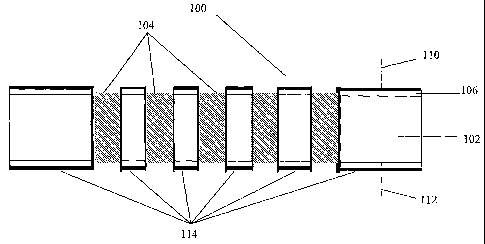
[0024] FIG. 1 is a cross-sectional view of a preconcentrator according to an
embodiment of the
present invention.
[0025] FIG. 2 is an electron micrograph of a cross-section of a
preconcentrator according to one
embodiment of the present invention.
[0026] FIG. 3 is a perspective view of a preconcentrator according to one
embodiment of the
invention.
[0027] FIG. 4 is a scanning electron micrograph of a preconcentrator according
to one
embodiment of the invention.
[0025] FIG. 5 is a cross-sectional view of the preconcentrator shown in FIG. 1
and illustrates a
method of using the preconcentrator according to one embodiment of the present
invention.
DETAILED DESCRIPTION
[0029] Reference will now be made in detail to the preferred embodiments of
the present
invention, examples of which are illustrated in the accompanying drawings.
FIG. 1 is a cross-
sectional diagram of a preconcentrator 100 according to an embodiment of the
present invention.
The preconcentrator 100 includes a substrate 102, illustratively, a
rectangular parallelipiped, with
passageways 104 running between top and bottom major surfaces, a conductive
material 106
covering the top and bottom major surface, except for the passageways, a top
electrical lead 110,
a bottom electrical lead 112, and an adsorbent coating 114 on the outer
surfaces of electrical
leads 110, 112. Top electrical lead 110 is connected to conductive material
106 on the top side of
the substrate. Bottom electrical lead 112 is connected to conductive material
106 on the bottom
side of the substrate. Electrical leads 110, 112 provide for passage of
current through the
conductive material and substrate so that the entire preconcentrator may be
used as a heating
element when a voltage is applied across conductive material 106.
[0030] Preconcentrator 100 is a three-dimensional preconcentration device with
an integral
heating element. The preconcentrator may be micro-machined or manufactured
using
conventional machining and techniques.
CA 02624262 2008-03-28
WO 2007/041551 PCT/US2006/038565
100311 "1 he exposed surface area of preconcentrator 100, to which the analyte
of interest
adsorbs as a sample passes through the preconcentrator, consists of the area
at the top and bottom
of the substrate 102 as well as on the inside surfaces of passageways 104.
Passageways 104 help
to maximize this exposed surface area and create a three-dimensional
adsorption surface. Thus,
preconcentrator 100 has an optimal exposed surface area, a large surface to
volume ratio, and an
extremely fast preconcentration time. In one preferred embodiment of the
invention, the
preconcentrator has an increased exposed surface area more than about twenty
fold when
compared to thin-substrate preconcentrators. In alternate enzbodiments of the
invention, the
preconcentrator has an increase in exposed surface area from about two fold to
about one
hundred fold when compared to thin-substrate preconcentrators.
[0032] In another embodiment of the invention, preconcentrator 100 is
substantially planar. In
an alternate embodiment, the preconcentrator has further surface features that
increase the total
exposed surface area: Differential etching of the substrate may create such
additional surface
features.
[00331 The preconcentrator may be fabricated in various thicknesses. In one
embodiment of
the invention, the preconcentrator has a thickness in the range from about 10
microns to about
1000 microns, alternatively from about 20 microns to about 150 microns,
alternatively from
about 125 microns to about 350 microns, alternatively from about 200 microns
to about 600
microns, alternatively from about 450 microns to about 750 microns,
alternatively from about
650 microns to about 1000 microns. In an alternate embodiment, the
preconcentrator has a
thickness from about 1 mm to about 50 mm, alternatively from about 2 mm to
about 11 mm,
alternatively from about 9 mm to about 20 mm, alternatively from about 15 mm
to about 25 mm,
alternatively from about 22 mm to about 30 mm, alternatively from about 28 mm
to about 39
mm, alternatively from about 37 mm to about 44 mm, alternatively from about 43
mm to about
50 mm. In another embodiment, the preconcentrator has a thickness from about
500 microns to
about 1500 microns, alternatively from about 550 microns to about 670 microns,
alternatively
from about 630 microns to about 760 microns, alternatively from about 740
microns to about 850
microns, alternatively from about 820 microns to about 930 microns,
alternatively from about
910 microns to about 1100 microns, alternatively from about 990 microns to
about 1120 microns,
alternatively from about 1110 microns to about 1240 microns, alternatively
from about 1230
microns to about 1390 microns, alternatively from about 1380 microns to about
1450 microns,
alternatively from about 1420 microns to about 1500 microns.
[0034] Advantageously, particularly for use in portable detectors, a
preconcentrator according
to the instant disclosure is extremely robust. The structure can be exposed to
much higher air
6
CA 02624262 2008-03-28
WO 2007/041551 PCT/US2006/038565
pressure, may suffer damage, and remain operable. This robustness is due to
substrate 102,
which is many times as thick as membrane substrates and extremely rigid
thereby creating a firm
mounting surface for the preconcentrator.
[0035] Substrate 102 may include any material that is rigid, can be micro-
machined, and is
strong enough to have a conductive material deposited on its surface. This
choice of material
allows the substrate to remain rigid despite having passageways. To facilitate
heating and reduce
power consumption, the substrate 102 ideally should not have a large thermal
mass. Examples of
suitable substrate materials include semiconductor substrates, such as e.g.
gallium arsenide or
silicon or dielectric materials such as glass, quartz, resins, and plastics.
In one embodiment, the
substrate is a metal. In another enlbodiment, the substrate is an SOI wafer.
In one embodiment,
the substrate is not highly insulating.
[0036] The passageways 104 in preconcentrator 100 may take many shapes other
than the
cylindrical holes shown in Fig. 1. Through use of semiconductor manufacturing
techniques, such
as deep reactive ion etching, the exact patterning of the passageways 104 can
be varied. In
another embodiment, the passageways are square holes. In another embodiment,
the
passageways are slots. In alternate embodiments, the passageways may be
serpentine channels.
[0037] The large amount of open area in the preconcentrator 100 created by the
passageways
104 results in a low-pressure drop across the substrate. This low pressure
drop makes the
preconcentrator particularly suitable for inline retrofitting to existing
detectors for most analytical
techniques such as chromatography, mass spectrometry, IMS and field asymmetric
ion mobility
spectrometry (FAIMS), without altering fluidics or changing existing pumps.
Thus, an existing
device can be preconcentrating, while operating in a normal detection mode,
thereby improving
the device's sensitivity. The pressure drop and flow rate related to an
interdigitated geometry is
given by the following equation:
Q=(N X'eVxh3XP)/(12x Lx(-t)
where: is dynamic viscosity (Air=1.808 10'S N s/m2 at 20 C)
N is number of drift regions in parallel
L is length of drift region (m)
h is height (m)
w is width of drift region (m)
Q is gas flow (m3/s)
P is pressure (N/m)
7
CA 02624262 2008-03-28
WO 2007/041551 PCT/US2006/038565
Based on the above equation, one of ordinary skill in the art can determine
the appropriate
dimensions of a preconcentrator according to the instant disclosure.
[0038] Conductive material 106 is a material (e.g, metal) that conducts
electricity. Similarly,
top electrical lead 110 and bottom electrical lead 112 are made from a
conductive material that
conducts electricity. Any conductive material known in the art is suitable for
the instant
disclosure. The conductive material may be, for example, gold, copper,
platinum, molybdenum,
titanium, chromiwn, tungsten, or combinations thereof. In one embodiment, the
conductive
material is a coated Ti barrier layer such as a Ti barrier layer coated with
Aluminum.
[0039] The electrical leads are connected to a power supply. Any power supply
known in the
art is suitable for the instant invention. In some applications, the power
supply is advantageously
a battery as the preconcentrator has low thermal mass. The optimal voltage to
be supplied by the
power supply depends on the choice of substrate and desired operating
parameters. In one
embodiment, the power supply applies from about 0.1 volts to about 100 volts,
alternatively from
about 0.5 volts to about 10 volts, alternatively from about 1 volt to about 15
volts, alternatively
from about 10 volts to about 25 volts, alternatively from about 20 volts to
about 50 volts,
alternatively from about 35 volts to about 80 volts, alternatively from about
55 volts to about 85
volts, alternatively from about 80 volts to about 100 volts the substrate. In
another embodiment
of the invention, the power supply is a battery.
[0040] In one embodiment particularly suitable for FAIMS, the power supply
applies from
about 0 volts to about 40 volts, alternatively from about 0.1 volts to about
0.5 volts, alternatively
from about 0.3 volts to about 1 volt, alternatively from about 0.9 volts to
about 10 volts,
alternatively from about 9 volts to about 15 volts, alternatively from about
13 volts to about 25
volts, alternatively from about 23 volts to about 35 volts, alternatively from
about 30 to about 40
volts.
[0041] A voltage applied between the electrical leads causes a current to
flow. This current,
without being bound by theory, leads to a Joule effect, which heats the
preconcentrator, thereby
leading to desorption of the analyte. The heating of the device is extremely
uniform, as the
conductive material creates an integral, continuous, distributed heating
element. Furthermore,
due to the low thermal mass of the preconcentrator, a low energy input is
necessary and heating
occurs quickly.
[0042] The adsorbent coating 114 covers conductive material 106 and the
interior surfaces of
passageways 104. By covering the conductive material and interior surfaces,
the adsorbent
coating causes the heating element to be an internal heating element. This
advantageously
maximizes heating while minimizing power consumption. The ability of the
adsorbent coating to
8
CA 02624262 2008-03-28
WO 2007/041551 PCT/US2006/038565
adsorb an analyte of interest depends on chemical selectivity, steric
selectivity or both.
Adsorbent coatings are commonly known in the art and any such coating may be
used
[0043] In one embodiment of the invention, the adsorbent coating is
polydimethylsiloxane
(PDMS)..
[0044] In some embodiments of invention, adsorbent coating 114 selectively
adsorbs a plastic
explosive or a chemical signature thereof. Thus, the coating may be selective
for e.g.
nitroglycerine (NG), dinitrotoulene (DNT), trinitrotoluene (TNT),
pentaerythritoltetranitrate
(PETN), cyclotrimethylenetrinitramine (RDX), trinitrophenyl-n-methylnitramine
(Tetryl), or
volatile taggant compounds such 2,3-dimethyl-2,3-dinitrobutane (DMNB) or
mononitrotoluene.
In other embodiments, the adsorbent is selective for a nerve agent such as
dimethyl methyl
phosphonate (DMMP).
[0045] In other embodiments of the invention, the adsorbent coating
selectively adsorbs an
illicit drug or a chemical signature thereof. For example, the coating may be
selective for mono-
and diterpenes released by marijuana, heroin, cocaine, or methamphetamines.
[0046] Analytes desorb from the adsorbent coating at different temperatures,
highly dependent
on the adsorption layer. Thus, by cycling through a series of desorption
temperatures it is
possible to desorb different classes of analyte over time. Such cycling
improves the selectivity
and reduces the effects of interferants. In one embodiment of the invention,
the adsorbent
coating is selective for two or more analytes of interest, which desorb at
different temperatures.
[0047] In one embodiment, the substrate is coated with one adsorbent coating.
In another
embodiment, the preconcentrator is coated with more than one adsorbent
coating. When the
preconcentrator is coated with more than one adsorbent coating, the coatings
are applied in such
a way that each coating occupies a unique area of the preconcentrator.
[0048] In another embodiment of the invention particularly suitable for
heating the inlet stream
that passes to the detector, the preconcentrator lacks an adsorbent coating.
[0049] In an alternate embodiment of the invention, the adsorbent coating has
a thickness from
about 0.001 microns to about 1 micron, alternatively from about 0.01 microns
to about 0.1
microns, alternatively from about 0.05 microns to about 0.3 microns,
alternatively from about 0.2
microns to about 0.6 microns, alternatively from about 0.5 microns to about 1
micron. In another
embodiment of the invention, the adsorbent coating has a thickness of about 1
micron to about 10
microns, alternatively from about 2 microns to about 7 microns, alternatively
from about 5
microns to about 10 microns.
[0050] FIG. 2 is a cross-sectional electron micrograph of the preconcentrator
according to one
embodiment of the invention. As shown in FIG. 2, preconcentrator 200 is a
layered substrate 202
9
CA 02624262 2008-03-28
WO 2007/041551 PCT/US2006/038565
with passageways 204. The layered substrate 202 includes a substrate with a
conductive material
coating on the top and bottom and an adsorbent coating on the entire surface.
In this embodiment
of the invention, the passageways 204 are slots. FIG. 2 illustrates how the
slotted passageways in
the substrate of the present invention create a large surface area to which an
analyte can adsorb.
100511 FIG. 3 is a perspective view of a preconcentrator according to one
embodiment of the
invention. A connecting bridge 118 connect the coated substrate 120 to a
holding frame 122.
The coated substrate 120 includes passageways therethrough, a conductive
material coating on
the top and bottom of the substrate, electrical leads, and an adsorbent
coating covering the top of
the conductive material and the inside surface of the passageways.
[0052] The connecting bridge 118 suspends coated substrate 120 in the holding
frame 122. The
connecting bridge 118 is thin so as to reduce heat loss to the holding frame,
thereby maximizing
the effect of heating the substrate and lowering power consumption. In one
embodiment, at least
two connecting bridges suspend coated substrate 120. In another embodiment,
only one
connecting bridge suspends the coated substrate. In an alternate embodiment,
at least four
connecting bridges suspend the coated substrate in the holding frame.
[0053] Holding frame 122 separates the analyte adsorbing area of the
preconcentrator from the
rest of the device. Thus, holding frame 122 and connecting bridge 118
thermally isolate the
coated substrate 120 from the surrounding device. This allows the heating to
be maximized and
reduce power consumption.
[0054] The holding frame 122 and connecting bridge 118 may be made from any
material that
is rigid and can be micro-machined. Advantageously, holding frame 122 and
connecting bridge
118 have a low thermal mass to further increase the device's efficiency.
Examples of such
materials include semiconductor substrates, such as e.g. gallium arsenide or
silicon or dielectric
materials such as e.g. glass, quartz, resins, or plastics.
[0055] In an alternate embodiment of the invention, two or more coated
substrates are
suspended within one holding frame. Each coated substrate contains a
substrate, passageways
therethrough, conductive material covering the top and bottom, adsorbent
coating, and electrical
leads as disclosed herein. By using several coated substrates, it is possible
to use different
adsorbent coatings with preferential selectivity for different analytes. Such
coated substrates are
comlected to each other and the holding frame by connecting bridges. Each
coated substrate can
be individually addressed electrically to cause heating. The thin connecting
bridges provide
thermal insulation thereby allowing independent operation. When a holding
frame is arranged in
such a way, a detection array is created. In one embodiment of the invention,
the coated
substrate contains a semiconductor substrate. In another embodiment, the
coated substrate
CA 02624262 2008-03-28
WO 2007/041551 PCT/US2006/038565
contains silicon. In an alternate embodiment, each coated substrate in the
array has an adsorbent
coating selective for a plastic explosive.
[0056] FIG. 4 is a scanning electron micrograph of one embodiment of the
preconcentrator
according to the invention. Clearly visible is the deeply etched structure of
preconcentrator 300
and.four tliin silicon connecting bridges 302. Also visible is silicon
substrate 304. The device of
FIG. 4 is incomplete. Prior to use, the remaining silicon substrate 304 would
be machined away
such that a gas stream could pass through the device.
[0057] For temperature sensing, a temperature variable thin-film resistor may
be patterned onto
the coated substrate. The resistance of this thin film structure changes with
temperature. The
temperature of the preconcentrator can be determined by measuring the
resistance, thereby
providing a measurement for closed loop control of the heated preconcentrator.
In one
embodiment of the invention, the preconcentrator further contains a single
thin-film resistor. In
another embodiment, the preconcentrator contains a plurality (iz. e., more
than one) of thin-film
resistors. The advantage of using a plurality of resistors is to ensure
temperature uniformity and
build in redundancy. Alternatively, the preconcentrator may lack a thin-film
resistor.
[0058] Use of a thin-film resistor enables closed loop operation. Thus, a
proportional-integral-
differential (PID) controller can be used to accurately control the
preconcentrator temperature.
The circuit formed by a thin-film resistor and controller can be directly
mounted on the ceramic
mount upon which the silicon die is fixed. In an alternate embodiment, the
preconcentrator
contains a plurality of thin-film resistors and a proportional-integral-
differential (PID) controller.
[0059] As previously discussed, the passageways in the preconcentrator may
advantageously
create a low-pressure drop across the preconcentrator, which makes it
particularly suitable to
retrofit to existing detection systems. For retrofitting, it may be desirable
to mount a
preconcentrator on a support, which is cheaper to produce than the
preconcentrator substrate,
such that the preconcentrator is properly placed inline with the existing
detector. A plurality of
preconcentrators may be mounted on a support and attached inline of an
existing detector. The
support may contain structural polymers such as TEFLON(R), ceramic or
polyetheretherketone
(PEEK). In one embodiment, the support may be of a standard size with an
adapter created for
an existing device. Thus, the same design of preconcentrator can be used with
many different
detectors, only requiring a change in the attachment adapter.
100601 FIG. 5 illustrates the method of using the preconcentrator of FIG. 1.
As described with
reference to FIG. 1, the preconcentrator 100 encompasses substrate 102 with
passageways 104
therethroi.igh, conductive material 106, top electrical lead 110, bottom
electrical lead 112, and
adsorbent coating 114. Arrow 116 indicates the flow of the analyte through the
three-
11
CA 02624262 2008-03-28
WO 2007/041551 PCT/US2006/038565
dimensional structure trom the top to the bottom. After the analyte is flowed
through the
preconcentrator and adsorbed for a predetermined preconcentration time, the
structure is heated
to release an analyte plume 118 into a detector. The method of using the
preconcentrator
comprises the steps of (a) contacting the analyte with the adsorbent coating;
(b) allowing the
analyte to adsorb onto the adsorbent coating; and (c) heating the
preconcentrator after a
determined period of time to release the concentrated plume of analyte into
the detector. In one
embodiment, the step of contacting is achieved by flowing gas through the top
of the
preconcentrator with the flow exiting through the bottom. The step of heating
the
preconcentrator is achieved by applying a voltage across the electrical leads
and allowing,
without being bound by theory, the Joule effect to heat the device.
[0061] In an alternate embodiment, the method further includes monitoring the
temperature of
the preconcentrator to ensure that the analyte of interest is released. In
that embodiment, the
preconcentrator contains at least one thin-film resistor and a proportional-
integral-differential
(PID) controller.
[0062] In another embodiment, the preconcentrator contains an adsorbent
coating that adsorbs
two or more analytes of interest, which desorb at different temperatures. In
that embodiment, the
step of heating the preconcentrator further includes cycling the
preconcentrator at the
temperatures at which the analytes of interest desorb.
[0063] As is well known in the art, only certain classes of analytes adsorb
onto the adsorbent
coating. This property combined with changing the initial air flow can be used
to improve the
selectivity and reduce the occurrence of false positives. In one embodiment of
the invention, a
preconcentrator is mounted inline of a detector, with an initial sample stream
passing parallel to
and over the preconcentrator, but not through it. As the analyte of interest
adsorbs to the
preconcentrator, interferants are not adsorbed and continue on their path out
of the device
without ever contacting the inline detector. After a defined preconcentration
period, a stream of
air is directed to pass through the preconcentrator and the analyte of
interest is desorbed from the
concentrator stream into the stream that leads to the inline detector. This
particular embodiment
is especially useful in military warfare agent detectors, when the adsorbent
coating selectively
adsorbs nerve agents. In a warfare environment, diesel, gasoline and jet fuels
all cause
significant false alarms when testing for nerve agents.
[0064] The preconcentrator according to the instant disclosure can be used for
many detectors.
The preconcentrator is useful for any detection technique that can benefit
from use of a
preconcentrator. In one embodiment, the preconcentrator is used inline for
IMS. In another
embodiment, the preconcentrator is used inline for FAIMS. In another
embodiment, the
12
CA 02624262 2008-03-28
WO 2007/041551 PCT/US2006/038565
preconcentrator is used inline for gas chromatography. In another embodiment,
the
preconcentrator is used inline for mass spectrometry.
[0065] Standard IMS typically involves heating of the analyte to make the
system more robust
against enviromnental variation. Heating is also desirable to prevent analytes
from sticking to
the apparatus before they reach the detector. The intrinsic heating ability of
a preconcentrator
according to the instant structure can be used to heat the analyte for IMS.
Such inline heating is
much more efficient as more of the analyte is heated. The surface area in
contact with the flow is
much greater allowing for greater heat transfer. In one embodiment of the
invention, a
preconcentrator according the instant invention is used as an inline heater
for standard IMS. In
another embodiment, a preconcentrator lacking an adsorbent coating is used as
an inline heater
for standard IMS.
[0066] The three-dimensional structure of a preconcentrator according to the
instant disclosure
complicates preconcentrator manufacture. The three-dimensional features need
to be coated with
the adsorbent coating. In some embodiments, the layer is uniform. Thus,
special manufacture
techniques are required. One technique suitable for applying is liquid source
misted chemical
deposition. Misted chemical deposition converts a liquid source material into
a very fine mist.
Nitrogen then carries this mist to a deposition chamber. In the deposition
chamber, sub-micron
droplets coalesce on the wafer thereby covering it with a uniform liquid film.
This film is then
thermally cured leaving a thin surface layer of solid. Thus, this technique
allows for a uniform
coating of a three-dimensional structure. One embodiment of the invention is a
method of
manufacturing of a preconcentrator comprising the steps of: a. supplying a
substrate; b. providing
passageways through said substrate; c. coating the top and bottom of said
substrate with a
conductive material; d. coating the entire substrate with adsorbent coating
using misted chemical
deposition. The method may further include the step of attaching electrical
leads to the
conductive material.
[0067] In one embodiment of the invention, the mist deposited has a droplet
size from about 0.1
microns to about 0.3 microns, alternatively from about 0.15 microns to about
0.27 microns. In
another embodiment, the method further includes the step of mounting the
substrate in a holding
fran1e.
[0068] As the present invention may be embodied in several forms without
departing from the
spirit or essential characteristics thereof, it should also be understood that
the above-described
embodiments are not limited by any of the details of the foregoing
description, unless otherwise
specified, but rather should be construed broadly within its spirit and scope
as defined in the
appended claims, and therefore all changes and modifications that fall within
the metes and
13
CA 02624262 2008-03-28
WO 2007/041551 PCT/US2006/038565
bounds of the claims, or equivalence of such metes and bounds are therefore
intended to be
embraced by the appended claims.
14