Note: Descriptions are shown in the official language in which they were submitted.
CA 02626360 2008-04-17
WO 2007/056314 PCT/US2006/043238
TITLE OF THE INVENTION
POWER CONVERSION REGULATOR
WITH PREDICTIVE ENERGY BALANCING
CROSS-REFERENCE TO RELATED APPLICATIONS
[0001] The present application claims the benefit of U.S. Provisional
Application Nos.
60/734,068, filed on November 7, 2005, 60/739,564 filed on November 23, 2005,
60/771,769
filed on February 9, 2006, 60/774,413 filed on February 17, 2006, all of which
are incorporated
herein by reference.
STATEMENT REGARDING FEDERALLY
SPONSORED RESEARCH OR DEVELOPMENT
[0002] The present invention was not developed with the use of any Federal
Funds, but was
developed independently by the inventors.
CA 02626360 2008-04-17
WO 2007/056314 PCT/US2006/043238
BACKGROUND OF THE INVENTION
[0003] It is often desirable to convert electrical energy sources from some
arbitrary voltage to
another arbitrary voltage or current. With high enough input voltages, simple
linear regulation is
often adequate, but often wastes power. For higher efficiency, and for
voltages or compliances
higher than the input voltage, either the input energy must be AC, or if DC,
it must be chopped
into AC.
[0004] In addition to input variations that must be regulated out, the
apparatus for such power
conversion usually introduces additional inaccuracies to their output
voltages, and usually adds
noise related to a chopping or to a mains frequency. This noise usually has
fundamental, lower
harmonic, and sub-harmonic components usually called "ripple," and higher
harmonic
components related to the edge-rate of chopping that cause Electro Magnetic
Interference, or EMI.
[0005] Regulators are also usually required to maintain their outputs constant
despite changes
of their loads. For such applications as Voltage Regulation Modules, or VRM's,
for computers,
regulators may be required to respond to both desired output voltage changes
and to load changes
from near-no-load to near-full-load in microseconds.
[0006] Traditionally, large output filter capacitors have absorbed sudden load
changes and
filtered out ripple, and fairly simple feedback loops have been used to
control regulator output
voltage or current, and impedance at low frequencies, but large-value
capacitors are physically-
large, expensive, and resist nimble voltage control.
[0007] Most traditional control loops*have depended upon significant Effective
Series
Resistance, or ESR, of filter capacitors to allow into their feedback loops a
small amount of high-
frequency ripple, which has been applied to lead networks to stabilize their
control loops.
2
CA 02626360 2008-04-17
WO 2007/056314 PCT/US2006/043238
[0008] Beyond the frequencies where practical gain-bandwidths enable active
control of
output, the minimum amount of ripple on the output of a switching regulator is
set by the equation
dV=I*dT/C, where V is the output voltage in volts, I is the load current in
amperes, T is the time
in seconds, and C is the filter capacitor in farads. A good regulator would
produce only the
amount of ripple indicated by that equation.
[0009] Unfortunately, ESR related ripple contains two additional ripple
components ESR*Im
and ESR*ll where, ESR is that of the filter capacitor, Im is the stroke of
current that replenishes
the energy of the capacitor, and Il is the load current. Unless the complexity
of post-filtration is
added, both the additional ripple and EMI of ESR*Im ripple pass out of the
regulator. Prior art
regulators that require ESR for their stability often incur the expense and
complexity of additional
filtration to abate EMI.
[0010] Recently, relatively large monolithic ceramic capacitors with low ESR
have become
coirunon. Such near-ideal capacitors can, in principle, reduce ripple to the
theoretical, reducing
post filtration for abatement of EMI up to above their self-resonant
frequencies where they appear
inductive. However, the practical application of these near-ideal filter
capacitors has been
troublesome. They form at the regulator output a near-ideal pole that many
prior art regulators
have difficulty compensating without compromise.
[0011] Some earlier regulator designs simply oscillate unless these capacitors
are degraded
by adding series resistance. Some regulators may be stabilized by an
additional pole significantly
?0 lower in frequency than the output pole, but with loss of transient
response. Some compensation
schemes suppress enough of the wrinkles of their Bode plots to achieve some
stability together
with decent transient response, but the range of inputs and load over which
they are absolutely
stable is often limited, and outside that range they often produce sub-
harmonic ripple tones that
3
CA 02626360 2008-04-17
WO 2007/056314 PCT/US2006/043238
make their ripple larger than the theoretical minimum. Some relief has been
afforded by the
addition of ramp waveforms to regulator control loops. Many of these prior-art
solutions lack
universality of application, requiring strict application rules to be
followed, or the expense of a
custom application design to be incurred. One prior-art solution for
stabilizing regulators involves
adjustment of a "tuning" resistor to the intended application.
[0012] It is also common for the stability and transient response of earlier
regulators to be
predicated upon a fixed, known, and stable filter capacitance. Many modern
loads include
unknown capacitance, creating an application difficulty for regulators that
are capacitance-
sensitive, a problem that is exacerbated by the recent practice of "hot-
swapping."
[0013] The advent of low ESR filter capacitance has engendered another problem
that for
buck-converters may be as severe as energy-balance problems. The L-C filters
of such converters
often constitute lumped-element transmission-lines that were in times past
substantially
terminated by the ESR's of filter capacitors. With low ESR capacitors,
resonances and reflections
may occur within these transmission-line sections, upsetting loop stability
and degrading transient
response
[0014] The problems cited above are occasioned by the prior-art practice of
attempting to
regulate voltage without addressing the stored energy of regulator components.
BRIEF DESCRIPTION OF THE INVENTION
[0015] A power-conversion regulator comprising an inductive reactor, an output
filter reactor,
and a switch for admitting energy to the inductive reactor, additionally
comprises computation
circuitry responsive to the flux in the inductive reactor, to a reference
signal, to an output voltage,
and sometimes to an output load current, for computing the quantity of energy
that must be
supplied to a load and to the output filter reactor to regulate the output
voltage or current to a
4
CA 02626360 2008-04-17
WO 2007/056314 PCT/US2006/043238
desired relationship with the reference signal during each chopping waveform
cycle driving the
switch. As the inductive reactor is charged from an input energy source, the
computation circuitry
predicts whether the energy in the inductive reactor has become adequate for
the regulation. The
computation circuitry predicts the energy that is adequate for regulation, and
activates the switch
for sufficient time adequately to charge the inductive reactor. The
computation circuitry may also
turn off the switch at a time in a the cycle when insufficient tiine remains
within the cycle for the
inductive reactor to deliver to the load and to the output filter reactor
capacitor any additional
energy with which it might otherwise be charged. The regulator of this
invention may also
comprise circuitry for determining the value of the inductive reactor. The
regulator of this
invention may also comprise circuitry for determining the value of capacitance
included within
the regulator and attached to its output. The regulator of this invention may
also comprise
circuitry for terminating transmission-line effects of L-C filters.
BRIEF DESCRIPTION OF THE DRAWINGS
[0016] Figure 1 illustrates a flyback-type converter of the present invention.
[0017] Figure 2 shows waveforms of the regulator of Fig.1 being exercised with
load and
capacitance changes at its output terminals.
[0018] Figure 3 is a schematic diagram of a simplified flyback converter
according the
present invention.
[0019] Figure 4 shows the transient response of the regulator of Fig. 3 when
its load is
abruptly exercised.
[0020] Figure 5 shows the ripple of the regulator of Fig. 3 whilst its load is
gradually
exercised.
5
CA 02626360 2008-04-17
WO 2007/056314 PCT/US2006/043238
[0021] Figure 6 illustrates a method of fitting a flyback-type converter
according to this
invention with components to provide a galvanic isolation barrier between its
input terminals and
its output terminals.
[0022] Figure 7 illustrates a flyback-type converter comprising a
asynchroiious regulator of
the present invention, having a servo-loop for its capacitive energy term,
[0023] Figure 8 illustrates the output waveform as the regulator of Fig. 7 is
exercised by a
ramp load change and by a capacitance change.
[0024] Figure 9 illustrates a flyback-type converter comprising a asynchronous
regulator of
the present invention, having a simplified servo-loop for its capacitive
energy term
[0025] Figure 10 shows the waveforms of Fig. 9 as the latter is exercised by
load current and
capacitance changes.
[0026] Figure 1 I illustrates a flyback-type converter comprising a
asynchronous regulator of
the present invention.
[0027] Figure 12 shows the output waveform of the regulator of Fig. 11 when
the latter is
exercised with the ramp load current.
[0028] Figure 13 shows the output waveform of the regulator of Fig. 11 when
the latter is
exercised with a varying input voltage.
[0029] Figure 14 illustrates a buck-type converter into which the regulator of
the present
invention has been included.
[0030] Figure 15 illustrates wavefoims generated by the buck converter of Fig.
14 as it is
exercised by a varying load and by a switched capacitance.
6
CA 02626360 2008-04-17
WO 2007/056314 PCT/US2006/043238
[0031] Figure 16 illustrates the Vo(t) waveform generated by the buck
converter of Fig. 14 as
it is exercised by a time-varying input voltage.
[0032] Figure 17 illustrates a buck converter equivalent to that of Fig. 14,
but embodied using
digital rather than analog techniques.
[0033] Figure 18 illustrates AC peak-to-peak to DC voltage converters for use
in inductance
meters.
[0034] Figure 19 illustrates AC peak-to-peak to DC voltage converters for use
in capacitance
meters.
[0035] Figure 20 illustrates a loadmeter for use in buck regulators of the
present invention.
[0036] Figure 21 illustrates a current-output regulator according to the
present invention.
[0037] Figure 22 shows the current output waveform of the regulator of Fig.
21.
DETAILED DESCRIPTION OF THE INVENTION
[0038] A power-conversion regulator including an input adapted to receive
energy from an
energy source, an inductive reactor for energy storage, a switch to charge
said inductive reactor
with a desired quantity of energy from said energy source, an output filter
reactor for output
filtration, and an output adapted to supply energy to a load. Said regulator
may be used to
regulate the output of a DC-to-DC power converter wherein both the energy
source and the output
voltage or current are substantially steady, or of an AC-to-DC converter
wherein the input energy
source is already cyclically undulant, and may be embodied either as an
integral part of such
converters or independently embodied. It should be noted that whilst
commencing a chopping
cycle by charging the inductive reactor and continuing so to charge it until
it holds the predicted
required energy incurs minimal prediction time and is simplest to implement,
there is an alternate
7
CA 02626360 2008-04-17
WO 2007/056314 PCT/US2006/043238
and less preferred method for practicing energy balance according to this
invention. This latter
method comprises:
predicting energy demand for an ensuing chopping cycle and commencing said
chopping
cycle,
calculating the needed inductive reactor charging time,
subtracting the needed inductive reactor charging time from the entire
chopping cycle to
obtain a time difference,
delaying inductive reactor charging from the start of the chopping cycle by
said time
difference and,
terminating inductive reactor charging at the end of the chopping cycle.
It should be understood that, according to this latter method, the time for
discharging the inductive
reactor follows the commencement of the charging cycle and precedes
commencement of an
inductive reactor charging time.
[0039] If said energy source is substantially DC, the regulator of this
invention also comprises
an AC signal for chopping. Whether said AC signal is derived from a separate
source or from
said mains, it will be called, a"chopping" signal, and the terms frequency,
cycle, and period, will
be understood to relate to said aspects of said signal. Said signal may also
be used to supply a
time variable to computation circuitry described hereinbelow.
[0040] It should be understood that all signals of the present invention may
be represented by
analog or digital quantities, and that all computations may be implemented by
analog or digital
circuits, or by combinations thereof.
[0041] Though many embodiments of this invention illustrated hereinbelow are
synchronized
by a fixed chopping signal, it should be understood that this invention may be
practiced without
8
CA 02626360 2008-04-17
WO 2007/056314 PCT/US2006/043238
such rigid clocking, provided that the energy balance, to be more fully
discussed hereinbelow, is
ascertained and is addressed by said computation circuitry.
[0042] Said regulator also receives a reference signal to which said
regulator's output is
compared to provide a desired output. The invention also may include a circuit
to produce a flux
signal having a known mathematical relationship with the energy of said
inductive reactor's
magnetic field, and circuitry to produce an output signal having a known
mathematical
relationship to the voltage or current at said regulator's output.
[0043] Said regulator further includes computation circuitry responsive at
least to said flux
signal, or a prediction thereof, to said reference signal, and to said output
signal, for predicting the
quantity of energy that will be required to maintain said output in a desired
mathematical
relationship with said reference signal at a point during a cycle. An output
of said computation
circuitry controls said switch to charge said inductive reactor with
substantially that quantity of
energy required to maintain said regulator output in desired mathematical
relationship with said
reference signal. Said computation circuitry may be integrated with either or
both said flux and
output signals, or may be separately embodied.
[0044] Said computation circuitry may also comprise turn-around circuitry to
terminate
charging of said inductive reactor should there occur a condition wherein
additional charging of
said inductive reactor does not yield additional available energy for
regulator output.
[0045] Within a cycle, and cycle by cycle, the computation circuitry of the
present invention
predicts energy required accurately to charge said inductive reactor.
Computation and control
according to this invention reduces regulator control-loop delay. Reduction of
said delay
substantially eliminates from said computations of said control-loop an output
filter reactor pole
that would otherwise limit regulator performance. Substantial elimination of
said pole allows the
9
CA 02626360 2008-04-17
WO 2007/056314 PCT/US2006/043238
output ripple of the regulator of this invention to be made substantially
equal to the theoretical
minimum described herein. Substantial elimination of said pole also endows
this regulator with
excellent transient response whilst simultaneously allowing the use of low ESR
capacitors,
minimizing sub-harmonic tones, and minimizing post-filtration requirements.
[0046] The regulator of this invention may be embodied within various types of
converters,
some commonly known as "flyback", "buck", "boost", or "sepic", provided that
converter
operation is predicated upon a substantial fraction of output energy being
transferred from input
to output through the flux of said inductive reactor. Adaptation of
embodiments is accomplished
by designing said computation circuitry with algorithms appropriate for the
type of converter to be
regulated.
[0047] The regulator according to this invention may be made to operate in
either the
"discontinuous" or "continuous" modes well known in the art, or in both, its
inductive reactor
current either becoming or not becoming, equal to, or less than, zero during
each cycle.
[0048] The regulator of this invention may be embodied in either single-phase
or multi-phase
converters, such converters themselves being well known.
[0049] The inductive reactor of this invention may be either a simple inductor
or a
transformer, allowing this invention to be practiced in either or both
isolated and non-isolated
converters.
[0050] To facilitate the use of the actual, rather than nominal, value of said
inductive reactor
10 as a variable in the determination of its energy, the regulator of this
invention may comprise
circuitry for determining actual inductance of said inductive reactor.
CA 02626360 2008-04-17
WO 2007/056314 PCT/US2006/043238
[0051] Likewise, to facilitate the use of the actual value of capacitance,
both contained within
and/or attached to its output, as a variable in the determination of its
energy, the regulator of this
invention may comprise circuitry for determining said actual capacitance.
[0052] The regulator of the present invention may be fitted with circuitry to
determine the
value of its load current.
[0053] The regulator of the present invention may be fitted with circuitry to
terminate any
lumped-element transmission-line formed by L-C filters contained therein or
applied thereto.
[0054] The regulator of this invention is shown embodied in several types of
converters. The
regulator of the present invention is applicable to power converters in which
a significant fraction
of output energy is transported from input to output through the flux of an
inductive reactor.
[0055] The present invention is practiced when the energy required to supply
said load and to
replenish said output filter reactor to maintain a desired output voltage or
current is calculated
and substantially that amount of energy is charged into said inductive
reactor, thus maintaining
energy balance.
[0056] The fundamental equations for energy are:
for the energy in the inductor: KE=(L*I~2)/2 (Equation 1)
and for the energy in the capacitor: KE=(C*E~2)/2 (Equation 2)
where: KE is kinetic energy in joules
E is voltage in volts
1 is current in amperes
L is inductance in henries
C is capacitance in farads
And the A symbol indicates raised to the power of the following number (here
indicating the
power of 2).
11
CA 02626360 2008-04-17
WO 2007/056314 PCT/US2006/043238
[0057] The more accurately these energies are calculated, the more closely
will output
ripple approach the theoretical minimum governed by the equation:
dV=I*dTIC (Equation 3)
where: V is the output voltage in volts
1 is the load current in amperes
dT is the time in seconds between replenishments of filter capacitor energy
C is the filter capacitor in farads
dV being output ripple voltage.
[0058] A very good regulator would produce only the amount of ripple indicated
by equation
3. Slight inaccuracies of energy calculation in embodiments of the present
invention give rise to
minuscule variations of ripple that occur at half the chopping frequency, i.e.
its Nyquist
frequency.
[0059] Predicting said required energy is the task of signal conditioning and
computation
circuitry. A reference signal provides a goal in accordance with which this
regulator strives to
maintain its output. Output signal sensing presents said computation circuitry
with a useable
representation of said output. The computation circuitry predicts how much
energy within a cycle
will be required to maintain regulation.
[0060] Not only must said computation circuitry monitor energy demand, but
also it must
monitor or predict stored energy. Since at least part of the stored energy
resides in the field,
circuitry for providing a signal responsive to the magnetic flux of the
inductive circuitry reactor is
included. Three ways to practice flux determination according present
invention are:
1. determination of the energy contained in said inductive reactor's magnetic
field by
measurement of that field. Hall-effect and GMR devices capable of making this
measurement are well known or,
12
CA 02626360 2008-04-17
WO 2007/056314 PCT/US2006/043238
2. measurement of the current in a winding of, or magnetically coupled to,
said inductive
reactor. In this case the inductive reactor acts as its own integrator,
drawing a current
closely related to the voltage-time product having been applied thereto or,
3. computational determination of the energy contained in said inductive
reactor's
rriagnetic field by integration of the voltage-time product applied thereto.
These methods are exemplary and other methods for determining flux are also
within the scope of
this invention.
[0061] To accurately predict energy demand and supply, the computation
circuitry may also
addres,s a time variable. For instance, because time within a cycle elapses as
said inductor is being
charged, and it is impractical to discharge it forever, a finite time remains
to discharge and obtain
energy from said inductive reactor. If the value of said inductive reactor be
L, the voltage into
which said inductive reactor must be discharged be Ed, the time available to
discharge be dT,
then the amount of current by which said inductive reactor may be discharged,
dIL, is governed
by the equation:
dIL=Ed*dT/L (Equation 4)
[0062] If an instantaneous current in said inductive reactor be IL(t), then
the current after
discharge, IL(d,) for the available time will be:
IL (d) = IL (t) - dIL (Equation 5)
[0063] Applying equation 1, to both IL(t) and IL(d) and subtracting the latter
result from the
former result predicts the energy that said inductive reactor will yield by
the end of discharge
within the cycle.
13
CA 02626360 2008-04-17
WO 2007/056314 PCT/US2006/043238
[0064] Since, in asynchronous embodiments of this invention, the inductive
reactor may be
discharged for as long as desired to return it to a desired current, the
inductive energy in such an
embodiment may be simpler, and need not be time-related.
[0065] The prediction of energy required by, or supplied by, said filter
capacitor is simpler,
and is based upon the sum of regulator internal capacitance and load
capacitance externally
connected thereto. If C be said capacitive sum, Eref be a desired output
voltage at a point in a
cycle, and Eo(t) be an instantaneous output voltage, applying equation 2 to
both voltages and
subtracting the latter result from the former result predicts the energy that
this capacitance will
yield or absorb.
[0066] A third energy term predicts the energy that will be required by the
load during time
being predicted, which is simply the product of present output voltage,
present output current, and
time remaining in the present cycle This term may not be explicitly addressed
in asynchronous
embodiments of this invention.
[0067] In flyback converters, the time between prediction and attaining the
desired point is
often so short that this term may be ignored or replaced by a factor applied
to one of the other
energy terms. In the figures below, embodiments of this invention both
explicitly addressing, and
ignoring this term are shown. Inasmuch as it is usually undesirable to insert
a sampling resistor in
series with regulator output, load current in a buck regulator passes through
said inductive reactor,
and the current in said inductive reactor may be measured to determine its
energy, load current
information may be extracted from said inductive reactor's current data. Such
extraction may
performed by the computation circuitry described herein below or may be
separately embodied.
14
CA 02626360 2008-04-17
WO 2007/056314 PCT/US2006/043238
[0068] In addition to the aforementioned signals, said computation circuitry
may need to
determine the values of said inductive reactor and the aforementioned
capacitive sum. If these
values are known, they may be presented to said computation circuitry as
constants.
[0069] Because real inductors may vary from their nominal values and may vary
with current
and temperature, it is advantageous to include in the regulator of this
invention circuitry for
determining actual inductance of said inductive reactor. This determination
may be embodied
explicitly and ratiometrically by using a reference inductor sharing either
voltage or current with
said inductive reactor, or may be embodied implicitly within said computation
circuitry, or by
adjunct computation circuitry, by solving the equation L=E*dT/dI where: L=the
inductance being
determined, E=the voltage across said reactor during the determination time,
dT=the
determination time, and dI= the change of curTent in said reactor during said
determination time.
[0070] To compute an energy term, to be described below, of a flyback
regulator, and/or to
facilitate implicit determination of inductance as described above, it is
often necessary to make
regulator input voltage at least part of said "E". To this end, the regulator
of this invention may
also comprise input voltage measuring circuitry.
[0071] Likewise, not only do real capacitors vary from their nominal values
and vary with
voliage, but a typical load may include significant capacitance that should be
included in the
energy computation of the regulator of this invention. Moreover, the recent
prevalence of "hot-
swapping" may cause load capacitance to vary widely and suddenly. It is
therefore advantageous
to include in the regulator of this invention circuitry for determining actual
capacitance
therewithin and attached to the output thereof.
[0072] Just as inductive reactor value may be determined either explicitly or
implicitly, so
may the aforementioned capacitive sum be explicitly or implicitly determined.
Explicit
CA 02626360 2008-04-17
WO 2007/056314 PCT/US2006/043238
capacitance determination may be done ratiometrically by relating either total
ripple current or
output ripple current to the current in an internal filter capacitor of known
value. Implicit
capacitance determination is done by exploiting the fact that the capacitive
portion of the energy
balance of the present invention underlies its voltage regulation. Thus, if a
second, slower, control
loop be embodied to servo capacitance to that value which results in correct
output voltage, the
capacitance that it reports will reflect the total capacitance at the
regulator output. Not only does
this technique simplify capacitance measurement, but it also may yield line
and load transient
response superior to that obtained using capacitance as reported by a
ratiometer.
[0073] It should be noted that implicit capacitance determination rests upon
accurate inductive
reactor value determination. What is actually reported to the energy balance
of the computation
circuitry is L/C ratio. Inductance determination rests in turn upon accurate
knowledge of voltage,
current, and time, but the latter are usually easily determined with more than
adequate accuracy.
[0074] It should further be noted that though this invention is, for clarity,
presented in terms of
absolute values of such variables as time, voltage, current, inductance, and
capacitance, these
computations have mathematical equivalents that may be expressed in terms of
L/C ratio.
Therefore, even though, for thoroughness of explanation, some embodiments of
this invention are
shown with separately-reporting inductance and capacitance determining
circuitry, an adaptive
portion of said computing circuitry may operate according to this invention
with any adaptive
technique that results in control of inductive charging based on substantially
accurate energy
balance. Such techniques according to this invention may not even explicitly
report values of
components, as long as energy balance is thereby achieved.
[0075] Moreover it should be noted that either diodes or active switches may
be used for some
switching functions in converters. The voltage drops of such switches niay be
explicitly
16
CA 02626360 2008-04-17
WO 2007/056314 PCT/US2006/043238
calculated and entered into the aforementioned energy balance, but when such
losses are small it
often suffices to accommodate these slight losses and those of snubber
networks by slightly
adjusting one of the energy terms that requires explicit computation.
[0076] Moreover, it should be noted that though the feedback loop delay of
this invention is
much reduced below that of prior art, the relationship between control and
output is discontinuous
for at least very short times, which makes this regulator a sampled system.
Like many sampled
systems, this regulator may yield its cleanest output with excellent transient
response when its
loop gain is slightly less than unity. When said loop corrects most of its
error within a cycle, its
transient error is minuscule compared to its theoretical minimum ripple. Said
loop is robust,
allowing approximate calculation to be compensated by lower gain.
[0077] Said computation circuitry is inutile unless it performs its most
important function,
which is controlling the charging of said inductive reactor. Limitation of
charging may be done
under the three circumstances of:
1. attaining predicted energy balance,
2. occurrence of an inductive energy turnaround, as will be later described
hereinbelow,
3. mandatory reset to avoid excessive duty cycle that might endanger the
regulator or
allow ripple at an undesirably low frequency and may also be done if in the
event of an
under-or-over-voltage or over-current condition.
[0078] Charging is stopped by turning off the aforementioned switch under
control of said
computation circuitry. Said switch may be a semiconductor such as a BJT, a
MOSFET, and
IGBT, or a thyristor with needed commutation apparatus, Said switch may also
be embodied as a
saturable reactor such as is well known, to which magnetic bias may be applied
either suddenly or
gradually, and which may even be integral with said inductive reactor.
17
CA 02626360 2008-04-17
WO 2007/056314 PCT/US2006/043238
[0079] Additionally, circuitry is provided to avoid charging said inductive
reactor with energy
that cannot be quickly transferred to said regulator output. Early in a cycle,
as charging of said
inductive reactor begins, charging for additional time makes additional energy
available therefrom
later in that cycle. However, because without infinite voltage the current in
an inductive reactor
cannot be changed instantaneously, a turn-around point may be reached later in
a cycle when
insufficient time remains to extract increased energy from said inductive
reactor. Charging
beyond that point in time reduces available energy within that cycle. This
concern may be
ignored in asynchronous embodiments of the present invention. For this
purpose, stating that
there is no longer energy available is not meant to imply to that there is no
longer energy stored in
the inductor, but that there is insufficient time remaining in the cycle to
discharge any additional
energy being placed into the inductor.
[0080] Equations 4 and 5 show that as discharge time of said inductive reactor
approaches
zero, the current change that may be caused therein, and the energy that may
be extracted
therefrom also approach zero. At some point in any cycle, as inductive energy
increases whilst
the time to extract same decreases, said turn-around point may be reached.
[0081] Said turn-around circuitry is responsive, either directly or
indirectly, to a sign-change
of the slope of the change of available kinetic energy in said inductive
reactor, as determined by
equations 1, 4, and 5. Direct response is made by computation from those
equations, whilst
indirect response is made by computation based on the sign-change of the slope
of energy-
balance.
[0082] Implementation of a control loop that assumes that additional charging
produces
additional available energy may result in negative feedback and stable
operation up to said turn-
around point but, using such a loop, charging beyond said amount of energy
yields positive
18
CA 02626360 2008-04-17
WO 2007/056314 PCT/US2006/043238
feedback that may cause a regulator destructively to run away. Therefore the
computation
circuitry of the regulator of this invention may comprise turn-around
circuitry to terminate
charging of said inductive reactor should such a turn-around condition occur.
[0083] Said turn-around circuitry may be independently embodied within prior
art regulators
to prevent runaway. An aspect of the present invention is practiced when
charging of said
inductive reactor is terminated to avoid available-energy turn-around.
[0084] Turn-around prevention may be omitted from asynchronous embodiments of
the
present invention.
[0085] The regulator of this invention may be implemented with a capacitively
coupled
lumped-element transmission-line terminator to minimize lumped-element
resonance and
transmission-line reflections. A termination according to this invention may
comprise an extra
capacitor in shunt with normal filter capacitor or capacitors, its own ESR
having been selected
substantially to match the transmission-line impedance according to the
equation 2o=(LlC)~1/2,
Said termination may alternatively comprise said extra capacitor in series
with a discrete resistor,
non-linear resistive elements such as diodes or varistors, or an active
terminator comprising active
devices such a BJT's or FET's. The output terminal of a properly biased totem-
pole output stage,
well known in semiconductor amplifiers, can also act as a non-linear
terminating resistor
according to this invention. Alternatively, since the energy-balance equations
of this invention
address the energy of the transmission line formed by said inductive reactor
and internal and
external filter capacitance, an explicit terminator may be omitted, allowing
the computation
circuitry to effect the task of termination.
[0086] As may be seen from the above, and in the description of the various
embodiments
below, the basic process of this invention involves energy balancing, or more
specifically, the
19
CA 02626360 2008-04-17
WO 2007/056314 PCT/US2006/043238
charging of the inductive reactor so that the amount of energy placed into the
inductive reactor
during inductive reactor charging is based approximately upon a per-chopping-
cycle load energy
requirement. The "requirement" may be based upon actual energy use, energy use
during a
previous cycle, predicted use for the remainder of the cycle, or predicted use
for a future cycle.
The term "based approximately upon a per chopping-cycle load energy
requirement" may mean
several things including: 1) based upon an estimate of the energy required by
the output load, 2)
based upon an estimate of the energy required by the output load and the
output filtration reactor.
(The output filtration reactor will usually be a capacitor for voltage
supply/regulator and a
inductor for a current supply/regulator.)
[0087] As used herein, a "chopping cycle" is either the clocked period of a
synchronous
converter, or a non-coherent period which responsively occurs in the natural
operation of a non-
synchronous converter.
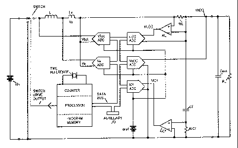
[0088] Fig. 1 illustrates a flyback-type converter comprising a synchronous
regulator of the
present invention, which operates as follows:
[0089] As in prior-art flyback regulators, one pole of an inductive reactor
(L) is connected
through sampling resistor RIL to one terminal of an input voltage source
(Vin). A switch '
cyclically and alternately connects a remaining pole of said inductive
reactance to a remaining
pole of said voltage source and through sampling resistor RIld to an output
filtration capacitance
and a load, which are in turn returned to said input voltage source. The duty-
cycle of this
switching relates an output voltage minus said input voltage to said input
voltage.
[0090] At this point we begin to depart from prior-art regulation techniques.
Whilst an
inductor L, comprising the sum of Lmain and Ls is connected between the poles
of said voltage
source Vin, its current, IL, rises. As IL rises, so does the kinetic energy
contained in the inductive
CA 02626360 2008-04-17
WO 2007/056314 PCT/US2006/043238
field. IL, passing through RIL drops a voltage proportional thereto. Amplifier
AIL generates a
voltage signal VIL(t) that represents the instantaneous value of IL.
[0091] Now we sharply depart from the prior art. VIL(t) is applied to both
inputs of multiplier
ILtSQ, which generates a signal VIL(t)~2 that represents the square of the
instantaneous value of
IL.
[0092] Since it usually is not practical or desirable to operate a flyback
converter at a low
frequency, there may be a limit set on the period of the cyclic switching of
the regulator. To begin
charging the inductor as just cited, a timing generator TIMEGEN sets a flip-
flop BISTABLE
which in turn connects said inductor L across Vin. At the same time, the
timing generator issues a
descending ramp waveform, VdT, that represents the time remaining in the
present chopping
cycle.
[0093] Since infinite time is not available to discharge the inductor L, and
neither is infinite
voltage available to discharge it in infinitesimal time, it may become
impossible to extract all of
the energy in its field in a given cycle. The remaining cycle time may cause
the discharged value
of IL, ILd, to be greater than zero current.
[0094] Since, upon switching to a discharging state, the inductor L will be
connected between
any voltage at the regulator output and the positive terminal of Vin, the
dominating voltage across
the inductor during discharge Vd will be the output voltage Vo(t), plus any
drop, Vdi, across
SWITCH in its "disc" position, minus VIN (-VIN). Summer VdSUM processes said
three
?0 quantities to produce a discharge voltage signal, Vd. If a synchronous
rectifier is used for the
"disc" pole of SWITCH, the term Vdi will likely be negligible, but if a diode
is used Vdi may be
important. In the latter case, a fixed value may represent diode drop, a
lookup table may return a
21
CA 02626360 2008-04-17
WO 2007/056314 PCT/US2006/043238
Vdi based on load current, or a similar diode driven by a load-related current
may be used to
produce Vdi.
[0095] Inductor L will be discharged from its present current IL(t) to ILd
according to the
equation ILd=IL(t)-V(d)*Tdisc/L).
[0096] Inductor L may discharge to zero current by the end of the present
chopping cycle. If
L is predicted fully to discharge, the quantity to be used for Tdisc is the
flyback time Tfb. To
produce a signal representing Tfb, VTfly, VIL, and a voltage representing
inductance, VL, are
applied to multiplier FLYMULT. Divider FLYDIV divides the output of FLYMULT by
Vd to
produce a signal VTfly in accordance with the equation dT=L*dI/E.
[0097] Said signal VL represents the value of the summed inductance of Lmain
and Ls. Ls is
an auxiliary inductor that comprises a standard for the ratiometric
measurement of Lmain. If the
value of Lmain is adequately known and stable, Ls may be omitted along with
inductance meter
ratiometer RATIOL, and a constant signal VL may represent L in the
calculations according to
this invention.
[0098] If VTfly exceeds VdT, insufficient time remains within the present
cycle fully to
discharge inductor L, in which case VTF is not the appropriate signal to use
to predict the
discharge of L. In this latter case, VdT is the appropriate signal to use to
predict the discharge of
inductor L.
[0099] A Tdisc selector selects the lesser of VTfly or VdT to produce a
discharge time signal,
VTdisc, representing discharge time.
[0100] To obtain a signal VILd predicting the current in L at the end of the
present cycle, V(d)
and VTdisc are applied to the inputs of inductor discharge multiplier LdMULT.
Inductor
22
CA 02626360 2008-04-17
WO 2007/056314 PCT/US2006/043238
discharge divider LdDIV divides the output of LdMULT by VL to produce a signal
predicting the
change of current in L were discharge to commence immediately and continue
until the end of the
selected discharge time. Subtractor LdSUBT subtracts the latter signal from
VIL(t) to produce a
signal VILd predicting the current in L were discharge to commence immediately
and continue
until the end of the selected discharge time.
[0101] VILd is applied to both inputs of multiplier ILdSQ which generates a
signal VILd~2
that represents the square of the predicted discharged value of IL.
[0102] Subtractor LSUBT generates a signal representing the difference of
VIL(t)~2 and
VILd~2 which is applied to one input of multiplier MULTL. VL is applied to the
other input
thereof, to yield a product, V2dKEL, which, when divided by 2, becomes a
signal VdKEL,
representing the kinetic energy predicted to be available from inductor L were
inductive discharge
to commence immediately and continue until the end of the selected discharge
time.
[0103] As L discharges, IL passes through VIN, through L and into both a load
RL and into an
internal filter capacitor Cf and any external capacitance Cext associate with
RL. Thus, during
discharge time, VIN is in series with the voltage generated by the flyback of
L, and thus VIN
contributes energy to the output. This energy is the product of VIN, the
average current in L
during discharge, and the time of discharge. Alternatively, load current and
the period of the
present cycle may replace the two latter terms to practice this invention. To
generate a signal
VKEINdisc predicting said energy from VIN, VIL(t) is multiplied by VTdisc by
multiplier
I*TMULT, and resulting product is then multiplied by VIN in multiplier
KEINMULT. The
output of I*TMULT is also passed to multiplier VKEdidiscMULT.
23
CA 02626360 2008-04-17
WO 2007/056314 PCT/US2006/043238
[0104] Summer SUPSUM adds VdKEL and VKEINdisc to predict the supply of energy
were
inductive discharge to commence inunediately and continue until the end of the
selected discharge
time, producing an energy supply signal, VKESUP.
[0105] Vo(t) has some instantaneous value that may be above, below, or equal
to
correspondence with a desired voltage, Vref, and an object of the present
invention is to cause
Vo(t) to correspond with said desired voltage at some time in the switching
cycle. This arbitrarily
chosen time is at the end of the cycle after the inductor has been charged and
discharged.
[0106] To this end it is desirable to predict how much energy the capacitance
will require to
be charged to a desired voltage were inductive discharge to commence
immediately and continue
until the end of the selected discharge time.
[0107] To this end, Vo(t) is applied to both inputs of multiplier VOtSQ to
generate a signal
[0108] Vo(t)~2 representing the square thereof. Vref is likewise applied to
both inputs of
multiplier VrefSQ to generate a signal VrefA2 representing the square thereof.
.[0109] Subtractor CSUBT generates a signal representing the difference of
Vo(t)~2 and
Vref~2 which is applied to one input of multiplier CMULT. A signal VC,
representing the sum of
regulator internal capacitance plus any external capacitance is applied to the
other input thereof, to
yield a product V2dKEC, which when divided by 2 becomes a signal VdKEC,
representing the
kinetic energy predicted to be required to charge total capacitance to said
desired voltage were
inductive discharge to commence inunediately and continue until the end of the
selected discharge
time.
[0110] If the value of Cf and any additional capacitance applied to the
terminals of the
regulator of this invention is adequately known and stable, a constant signal
VC may represent C
24
CA 02626360 2008-04-17
WO 2007/056314 PCT/US2006/043238
in the calculations according to this invention. If not, circuitry for
determining that total
capacitance will be discussed hereinbelow.
[0111] If a diode is used for discharging inductor L, a loss will be incurred
that consumes
energy. A signal VKEdidisc predicting this lost energy, were inductive
discharge to commence
immediately and continue until the end of the selected discharge time, is
produced by multiplier
VKEdidiscMULT. Where a synchronous rectifier is employed rather than a diode,
the signal
VKEdidisc, and the apparatus that produces it, may be omitted to practice the
present invention.
[0112] During discharge, as VIN and L are contributing energy, any load on the
regulator
output is simultaneously consuming energy. This load energy is predicted by
the equation:
i
KElddisc=Vo(t)*Iload*Tdisc (Equation 6)
where: Iload=load current.
[0113] If the load is substantially resistive, one may choose to obtain VIload
a signal
representing Iload, from a sampling resistor in series with the regulator
output, along with suitable
amplification, and thus practice the present invention. To address the likely
situation wherein the
load is reactive or that it is undesirable to apply a sampling resistor,
circuitry for implicitly
determining load current will be discussed hereinbelow.
[0114] Load current may be determined according to the equation
Ild=Ctot*Vrip/Tsag (Equation 7)
where:
Ild=load current
Ctot=total capacitance at the regulator output
Vrip=peak-to-peak output ripple voltage
Tsag=time of the cycle minus the discharge time of L
CA 02626360 2008-04-17
WO 2007/056314 PCT/US2006/043238
[0115] Combining the two equations above:
KElddisc=Vo(t) *Tdisc *Ctot*Vrip/Tsag (Equation 8)
[0116] Ripple P-P CONVERTER of conventional structure, comprising SWripa,
SWripb,Cripa, and Cripb converts Vo(t) to provide Vrip. This converter is
driven by a signal
VFBsw which is generated by a conventional comparator, FBCOMP, when Vfb, the
flyback
voltage of L exceeds a predetermined threshold voltage, VthFB.
[0117] To generate VKElddisc, a signal predicting the aforementioned energy to
be consumed
during discharge time, VC, Vo(t), Vrip, and VTdisc are applied to multiplier
KElddiscMULT, the
output of which is applied to divider KElddiscDIV, the quotient thereof being
the signal
VKElddisc.
[0118] Just as summer SUPSUM predicts the supply of energy, in like manner
summer
DEMSUM adds VdKEC, VKElddisc, and VKEdidisc to predict the demand for energy
were
inductive discharge to commence immediately and continue until the end of the
selected discharge
time, producing an energy demand signal, VKEDEM.
[0119] Balance comparator BALCOMP compares said predicted energy supply
signal,
VKESUP, with said predicted energy demand signal, VKEDEM. When the former
exceeds the
latter, BALCOMP generates a logical 1 at the input of OR gate ORRESET, which
in turn resets
BISTABLE, which in turn switches SWITCH to cominence the discharge of inductor
L.
[0120] In principle, there exists another energy loss term that is not
explicitly addressed in this
embodiment, that being the energy dissipated by any resistor of any snubber
network that may be
associated with inductor L. In practice, this energy has been found to be so
small as not to merit
26
CA 02626360 2008-04-17
WO 2007/056314 PCT/US2006/043238
explicit attention, and thus it exists as an insubstantial error in the
aforementioned energy terms
that are explicitly addressed.
[0121] TIMEGEN will set BISTABLE anew to begin a new cycle at the end of the
present
cycle. If flyback time equals or exceeds the remaining time of the present
cycle, this will occur
upon completion of the predicted and chosen discharge time. If however,
flyback time is less than
the remainder of the present time, the inductor L will conduct substantially
zero current until
charging commences in a new cycle.
[0122] Were energy balance the only reset term of the regulator of this
invention, this
regulator would share with prior-art regulators a propensity for destructive
runaway. The root of
this propensity is the fact that an inductor cannot instantaneously be
discharged without infinite
voltage or infinite time. At the commencement of inductive charge, additional
charging time
increases available inductive energy. However, if one persists in time to
charge the inductor until
the vol,tage-time product available for its discharge becomes insufficient to
discharge it, its
available energy begins to decrease with increased charging time. The energy
from VIN during
discharge time is also limited by discharge time. In this figure illustrating
the present invention,
the energy supply signal, VKESUP, is also fed to a slope detector comprising
differentiator CTA
and RTA along with comparator TACOMP. When the slope of VKESUP versus time
reverses, or
"turns-around", a signal VTA from COMPTA is applied to ORRESET, which in turn
resets
BISTABLE, which in turn switches SWITCH, terminating the inductor charging
cycle. The
turnaround aspect of the present invention contrasts with prior art in which a
certain slope of
feedback must prevail lest positive feedback incur destruction of the
regulator. Prior art usually
avoids turnaround by arbitrary limitation of duty-cycle or averts destruction
by limiting overall
current draw should turnaround occur, both of which approaches can incur
undesirable
27
CA 02626360 2008-04-17
WO 2007/056314 PCT/US2006/043238
inefficiency of operation. The turnaround aspect of this invention may be
practiced using
turnaround responsive either to VKESUP or VdKEL.
[0123] A method of generating VL as a function of inductance follows. Lmain
and Ls
together comprise a total inductance, L. Whilst the value of Lmain may be
modulated by
nonlinearities of the B-H curv.e of its core, Ls may be chosen to have smaller
inductance than
Lmain, perhaps 1% or 10% thereof, and thus it may drop but a small AC voltage.
If Ls be
suitably chosen, it will preferably rerirnain in a linear portion of its own B-
H curve at the current
where Lmain is approaching saturation. Ls may also be chosen to be as accurate
as desired.
Since 11 flows through both Lmain and Ls, a AC voltage Vtot is dropped across
their series
combination whilst a smaller voltage Vs is dropped across Ls. The ratio of
Vtot to Vs, provided
by divider LRATIOMETER, suitably scaled, provides a source of VL responsive to
the actual
value of Lmain plus Ls which may be used both for energy calculations
according to this -
invention and to warn that Lmain is either inadvertently of wrong value or is
approaching
saturation. Inductance may be determined by ratiometry using voltage ratios of
series-connected
inductors as shown, using current ratios of parallel-connected inductors or by
implicit
determination from volt-time product divided by current change as is shown in
another figure of
this invention. Whilst ratiometric determination of inductance is well-known,
its application to
energy calculation of energy in the control loop of a switching regulator is
an aspect of this
invention illustrated in this figure. Other circuitry for generating VL are
shown in more detail
hereinbelow in subsequent figures.
[0124] - Any of the embodiments described throughout this disclosure may need
to determine
11, the current in the inductive reactor, in order to determine the value of
the inductor reactor or the
flux stored therein. One method of so doing may be to employ a current mirror.
Current mirrors
28
CA 02626360 2008-04-17
WO 2007/056314 PCT/US2006/043238
are well known in the art, including the use of commercially available devices
such as
SENSFETs, HEXSENS, or mirrorFETs. Any other method of sensing current, whether
now
known or hereinafter invented is meant to be within the scope of the
invention. Similar
techniques and methods to any of those described herein may be used to
determine other currents
within the embodied circuits including current in the load or in the output
filter capacitor.
[0125] A method of generating VC as a function of capacitance follows. The
capacitance
capable of storing energy for prediction according to the present invention
comprises internal
regulator filter capacitance plus any capacitance connected to the regulator
output teiminals. The
switching cycle causes the AC current portion of IL which is divided between
internal and
external capacitance according to their respective susceptances. In this
figure, the discharge
current of L passing through a sampling resistor RIld, drops a voltage which,
amplified by AIld
and passing though high-pass filter HPF produces a signal VIld, which
represents the AC portion
of the load and filter currents, i.e., all the current flowing in the total
output capacitance. The
current if Cf passing through sampling resistor RICf drops a voltage that is
amplified by amplifier
AICf to provide a signal VICf, which is in turn applied to the divisor input
of divider
CRATIOMETER. Thus, by ratiometry, the AC portion of IL divided by the current
in Cf, if Cf be
accurately known, and the ratiometric output be suitably scaled, provides a
source of VC
responsive to the actual value of C, which voltage may be used for energy
calculations according
to this invention. Suitable dividend and divisor may be obtained using
sampling resistors,
amplifiers, and filters, as shown in this figure or by using current
transformers as shown below in
detail in another figure. Whilst ratiometric determination of capacitance is
well-known, its
application to energy calculation of energy in the control loop of a switching
regulator is an aspect
29
CA 02626360 2008-04-17
WO 2007/056314 PCT/US2006/043238
of this invention illustrated in this figure. Other circuitry for generating
VC are shown in more
detail hereinbelow in subsequent figures.
[0126] The reset signal of TIMEGEN may not always be vital to proper
operation, but may be
useful when the frequency of regulator output must be known, for example when
synchronous
operation of several regulators is desired.
[0127] In this embodiment, the computational functions shown are performed
using well-
known analog techniques. Addition and subtraction may be performed using some
of thousands
of species of well-known operational amplifiers. Multiplication and division
may be performed
using Gilbert-cell devices such as the Analog Devices AD734
multiplier/divider. Multiplication
and division may also be performed using well-known techniques exploiting the
predictable
logarithmic I/V behavior of BJT's. Alternatively, well known pulse-width
modulation techniques
may be used to perform the slower multiply/divide functions of this embodiment
such as
calculation of inductance and capacitance. All of these techniques may be
implemented using a
wide range of degrees of monolithic integration, from discrete components to
monolithic
integrated circuits. It is best to use fast techniques for calculation of
energy terms in the
computational paths responsive to VIL and Vo(t), inasmuch as delay generates
energy-balance
error. In the calculation of the energy terms of this synchronous embodiment
of this invention
"time is of the essence." Likewise, if excellent load transient response is
desired, fast techniques
are needed for predicting the load energy term of this embodiment.
[0128] Figure 2 shows waveforms of the regulator of Fig. 1 when it is
exercised with a ramp
load change between about 1mA and 40mA, and by a switched capacitance of 70 F
at its output
terminals, causing, with its internal 10 ,uF capacitor a total capacitance
change between 10 F and
80 ,uF. Ripple amplitude of output waveform Vo(t) is substantially inversely
proportional to total
CA 02626360 2008-04-17
WO 2007/056314 PCT/US2006/043238
capacitance. Since the desired voltage, in this case 5V, occurs in this
embodiment at the peak of
Vo(t) ripple, the top of Vo(T) remains substantially at 5V. The spikes
thereupon occur when
capacitance drops abruptly leaving, momentarily, an internal report of
capacitance far in excess of
the new true value. Moving down in the record is shown VC, the output of a
capacitance meter
comprised by this einbodiment of the present invention. Only the peaks of VC
are used to report
capacitance. Almost hidden below the ripples of VC is shown VL, the output of
an inductance
meter comprised by this embodiment of the present invention. VL is accurately
reporting an
internal inductance of 22 H. The waveform below is a separate report of Iload
because, despite
the internal existence of a term representing load energy during discharge
time, which contains
information about load current, there is no explicit term for Iload available
in the embodiment.
[0129] Figure 2, as well as all other graphs showing results of the invention,
are generated
using SPICE, a well known computer simulation tool for electrical circuits.
[0130] Figure 3 is both a SPICE and actual tested hardware schematic diagram
of a flyback
converter employing regulation according to a simplified form the present
invention. This
converter operates at an input voltage of 1.1 to 1.6 volts from VBat and
produces an output of 5V
with a power of 100mW into load Il. Ll, Q15, C4, C5, and R22 form an L-C
oscillator of
conventional character with a frequency of about 67 KHz. The output thereof is
AC coupled by
capacitor C7 to a sharpening and duty-cycle modifying circuit comprising Q14,
R14, R15, and
R17, all buffered by Ulb to provide a chopping signal. Ula provides for
enablement or
disablement of the converter. R18, Cl, and Ulc delay the rising edge of the
chopping signal to
prevent it from being confounded with and CLeaR signals to bistable U2a,b. To
increase output
drive, Bistable U2a,b is actually a single bistable made compound, of latches
that occur two per
package.
31
CA 02626360 2008-04-17
WO 2007/056314 PCT/US2006/043238
[0131] As the converter starts up and pumps up its output, the regulator is
restrained from
operation and the chopping signal passes at full duty cycle through bistable
U2a,b. The output
thereof drives a conventional flyback converter comprised of Q16, L2, R26, C8,
and D4, the latter
replenishing filter capacitor C6. C2 is a reservoir capacitor to supply local
energy to the flyback
converter and to provide a short AC return between L2 and ground. It should be
noted that D4
may be replaced by a well-known synchronous rectifier to practice this
invention. R25, Q17,
Q23, Q11, Q19, Q18, Q22, R32, R31, R29, R28, C13, C9, R23, R24, R10 and C10
form a current
monitor with a current sink output that is a replica of the current in Q16,
and of L2 during
inductor charge. Q3, Q6, Q5, Q7, Q9, Q10, Q8, and Q12, along with resistors
R5, R9, R11, R12,
R7, and form a voltage amplifier. D71eve1 shifts the 5V output to 2.5V with
ripple
superimposed. D8 is a 2.5-volt reference which is fed to the non-inverting
input of the amplifier
at the base of Q3. The shifted ripple on the - (that is, the negative) end of
V4 is fed though input
resistor R4 and speedup capacitor C11 to the base of Q6 which is the inverting
input of the same
amplifier. D6 prevents excess negative excursions of the amplifier output. R3,
R20, R21, Dl, D2,
and D3 form a curve-fitting feedback network to bend the replica of the ripple
to an
approximately square-root function. C2 adjusts the transient response of the
amplifier. Since the
amplifier is inverting, and referred to 2.5 volts, its output is a positive-
going bent, sawtooth wave
representing in the positive direction the square-root of the negative going
output ripple below 5
volts. The replica of inductor current sunk by Q22 develops a negative going
voltage drop across
R2. When that drop suffices bring the base of Q2 below 2.5 volts, the
comparator comprising Q1,
Q2, Q4, and R1 sources current to R8, producing a voltage which, passing
through nor gate Uld,
resets the bistable U2a,b, turning off Q16, thus terminating the charging of
L2 and initiating the
transfer of its energy to C6. Q13 clamps negative excursions at its emitter.
Q20, Q21, and Q24,
32
CA 02626360 2008-04-17
WO 2007/056314 PCT/US2006/043238
R27, R30, R33, and R34 illuminate LED D5 when the battery voltage falls below
1.1 volts, to
indicate the need to replace the battery.
[0132] Figure 4 shows the transient response of the converter and regulator of
Fig. 3 when its
load is abruptly changed from 1 mA to 19mA, and back to 1 mA.
[0133] Figure 5 shows the ripple of the converter and regulator of Fig. 3
whilst its load is
ramped from 0 mA to 20 mA. At full load, the theoretically minimum ripple' is
27.2 mV and the
ripple of the circuit of Fig. 2 is 27.4 mV.
[0134] Figure 6 illustrates a method of fitting a flyback-type converter
according to this
invention with components to provide a galvanic isolation barrier between its
input terminals and
its output terminals.
[0135] For this adaptation let it be assumed that the computation circuitry
shown in fig. 1 will
reside on the output side of said isolation barrier. The circuitry of Fig. 1
for predicting the signal
KEin should be removed or disabled, because in the isolated flyback converter
energy from the
input cannot cross the isolation barrier during flyback to appear at the
output. VIL(t) must be
adjusted to accommodate any turns-ratio applied, and VL must be adjusted to
accord with the
square of that ratio.
[0136] The isolation of Lmain is a simple matter, it simply gets another
winding to become a
transformer. If Ls is large relative to Lmain one may choose to make it also a
transformer of
turns-ratio equal to or properly related to the turns-ratio of Lmain and its
new winding. In this
case one may move the LRATIOMETER to the output side of the isolation barrier
as shown by
dashed lines.
33
CA 02626360 2008-04-17
WO 2007/056314 PCT/US2006/043238
[0137] Alternatively, if Ls be relatively small, one may retain the ratiometer
on input side and
pass VL across the isolation barrier using an isolation amplifier well known
in the art such as is
described in US Patent No's 4,395,647 and 4,383,222 or their more recent
counterparts, ADC's
and DAC's with optical or magnetic links, V-F and F-V con.verters with such
links, or one of a
plethora of other well-known isolation techniques.
[0138] VIN may be passed across the barrier using the same techniques as for
VL.
[0139] The passing of VIL(t) across the barrier is slightly more complex. The
chosen
isolation amplifier or other circuitry may not possess sufficient bandwidth to
pass this signal with
adequate fidelity. A current transfoimer might be used, but the latter is
implicitly a high-pass
filter, not passing DC information. A solution is to use both an isolation
amplifier or other
circuitry and a current transformer. In this figure current transformer TIL
with burden resistor
RILb can pass AC components of IL from about 1KHz to several hundred MHz. The
corner
frequency of TIL can be set by setting the time constant of its own inductance
divided by RILb.
The current IL also passes through RILa dropping a proportional voltage which
is fed to isolation
amplifier AISOIL that brings the DC information of IL across the isolation
barrier. The signs and
gains of the AC portion passing through TIL and the DC portion passing through
AISOIL should
be made properly to correspond, perhaps having equal gains and signs. The AC
and DC portions
of the IL information may be summed as shown or by many other well-known
circuits. If there
is overlap of the passbands of TIL and AISOIL, a low-pass filter ILLPF may be
used to remove
said overlapping response. Alternatively, if the corner frequencies of the two
paths be set equal,
ILLPF may be eliminated. Equalizing said corner frequencies produces a smooth
crossover
resulting an a substantially flat response from DC to a very high frequency.
[0140] An amplifier AIL may be needed properly to scale VIL(t).
34
CA 02626360 2008-04-17
WO 2007/056314 PCT/US2006/043238
[0141] Such a technique for conditioning VIL is also useful in non-isolated
converters where
relatively large voltages sometimes make galvanically-connected sampling of
the IL information
undesirable.
[0142] Figure 7 illustrates a flyback-type converter comprising a asynchronous
regulator of
the present invention, which operates as follows:
[0143] As in prior-art flyback regulators, one pole of an inductive reactor is
connected
through any sampling resistor, to one terminal of an input voltage source.
Switches, one of which
may be a diode, cyclically and alternately connects a remaining pole of said
inductive reactance to
a remaining pole of said voltage source and to an output filtration
capacitance and a load, which
are in turn returned to said input voltage source. The duty-cycle of this
switching relates an
output voltage minus said input voltage, to said input voltage.
[0144] Whilst an inductor L is charged, its current, IL, rises. As IL rises,
so does the kinetic
energy contained in the inductive field. IL, passing through RIL drops a
voltage proportional
thereto. Amplifier AIL generates a voltage signal VIL(t) that represents the
instantaneous value
of IL.
[0145] Now we depart from the prior art. VIL(t) is applied to both inputs of
multiplier ILtSQ,
which generates a signal VIL(t)~2 that represents the square of the
instantaneous value of IL.
[0146] Said signal VIL(t)~2, which is proportional to energy in inductor L, is
applied to one
input of divider KELSCL, and a scaling signal VKKEL is applied to the other
input thereof, to
yield a product, VKEL, representing the kinetic energy predicted to be
available from inductor L.
[0147] Output voltage Vo(t) has some instantaneous value that may be above,
below, or equal
to correspondence with a desired voltage, Vref, and an object of the present
invention is to cause
CA 02626360 2008-04-17
WO 2007/056314 PCT/US2006/043238
Vo(t) to correspond with said desired voltage at some time in the switching
cycle. This arbitrarily
chosen time is at the end of the cycle after the inductor has been charged and
discharged. To this
end it is desirable to predict how much energy the capacitance will require to
be charged to a
desired voltage were inductive discharge to commence immediately.
[0148] Since the ripple of the regulator of this invention is small, Vo(t)
contains a good
piecewise-linear approximation of the energy required to charge total
capacitance, Cf plus Cext, to
a desired voltage Vref.
[0149] Regulators according to this invention robustly attempt to restore
Vo(t) as just
described. Moreover, said regulators tend correctly to maintain energy balance
even when their
internal reports of inductance and capacitance are incorrect, as long as these
energies are reported
in substantially correct ratio. Inasmuch as the primary function of said
regulators is to regulate,
these propensities can be exploited to simplify regulators according to this
invention, albeit with
the loss of correct reports of inductance and capacitance, as will be
described hereinbelow.
[0150] Should the instantaneous voltage at VC incorrectly report the ratio of
inductance to
capacitance, the L/C ratio, Vo(t) fails correctly to correspond to Vref.
Subtractor dVSUBT
generates a signal VdV that represents the sign and the amount of the failed
correspondence, or
error. VdV is fed to one input of multiplier, VdVMULT, and a scaling voltage,
VKdV, is applied
to the other input of said multiplier, to generate a signal, VERRFRAC,
representing a
predetermined fraction of said error. The polarity of VERRFRAC is made to tend
to correct
errors of VC as follows. Sample-hold S+H, comprising BUFl, Shl, Chl, BUF2,
Sh2, and Ch2, of
conventional structure, stores the present value of VC for at least one cycle,
producing a signal
VCs 1. Summer CLOOPSUM adds VERRFRAC to VCs 1 to produce a new and more
correct
36
CA 02626360 2008-04-17
WO 2007/056314 PCT/US2006/043238
value of VC, which is used in a subsequent cycle. Thus errors in this
regulator's L/C ratio are
decimated within a few cycles to produce a corrected value of VC.
[0151] Said correct value of VC is applied to one input of multiplier KECMULT
whilst to the
other input of said multiplier VdV is applied. VdV contains information
proportional to the
amount of energy that will be required correctly to restore Vo(t) to proper
correspondence with
Vref. The product of this multiplication is the signal VKEC, that is
proportional to energy needed
properly to replenish the total output capacitance of the regulator according
to this invention.
VKEL and VKEC are applied to the inputs of energy balance comparator, BALCOMP,
which
produces a reset signal VRES when the former exceeds the latter. This reset
signal, passing
through an OR gate, ORRESET, resets a flip-flop, BISTABLE, which in turn opens
a switch,
SWITCH, terminating the charging and commencing the discharging of inductor L.
[0152] The other input of ORRESET is responsive to excess current in inductor
L, being
driven by a comparator ILHICOMP, which generates a reset whenever VIL(t)
exceeds a
threshold voltage VILthHI. This excess current reset function protects the
regulator from excess
current in accordance with prior art. Since, in this asynchronous regulator,
the time to discharge
inductor L may be made as long as is desired, there is no energy turnaround
such as is manifested
by synchronous regulators. In an asynchronous regulator, a current limit
suffices both to protect
components and to prevent undesirably long chopping cycles.
[0153] When charging is terminated, the current in inductor L continues to
flow, turning on a
diode D, or a synchronous rectifier, and supplying load current and
replenishing regulator output
capacitance. Signal VIL(t)is applied to one input a comparator, ILLOCOMP,
which generates a
set signal, VSET, whenever VIL(t) falls below a threshold voltage, VILthLO.
Thus, when
37
CA 02626360 2008-04-17
WO 2007/056314 PCT/US2006/043238
inductor L has been sufficiently discharged, BISTABLE is set, which in turn
closes SWITCH,
commencing another cycle by charging inductor L.
[0154] In turning on diode D when it supplies current, inductor L generates
voltage in excess
of Vo(t), and in excess of VIN. The inductor is said to "fly back" as it
discharges. The voltage of
inductor L is connected to one input of a comparator FBCOMP, to the other
input of which is
connected a threshold voltage, VthFB. FBCOMP thus generates a signal VFBsw
during flyback
time, i.e. the discharge of inductor L. Said signal VFBsw drives the switches
of the sample-hold,
S+H.
[0155] If VKKEL be correctly scaled to the actual value of L, the propensity
for the control
loop of the regulator of this invention to seek the correct output voltage
will cause a correct report
of total capacitance by the signal VC. If, however, VKKEL be mismatched to L,
this regulator
will still regulate well, but it will wrongly report the value of total
capacitance. In this case, its
transient response may be slightly degraded.
[0156] The signal VKdVSCL determines the fraction of error correction per
cycle. For
instance, a high value of VKdVSCL would result in quicker response to an
abrupt change in
capacitance, but with more likelihood of overshoot, whilst a low value would
produce slower
coirection without overshoot. One slight disadvantage of this embodiment
relative to more
complex embodiments is that the fractional per-cycle correction of its
capacitive feedback loop
limits the rate at which capacitance corrections can be made. This presents a
problem only when
sudden changes of capacitance are made. A sudden addition of significant
capacitance produces a
temporary output voltage droop and a sudden removal of significant capacitance
produces a
temporary output voltage spike. If said spike presents an application problem,
it is a trivial matter
38
CA 02626360 2008-04-17
WO 2007/056314 PCT/US2006/043238
to add a reset signal to ORRESET when output voltage exceeds desired voltage
by a chosen
fraction.
[0157] The propensity of the energy balance feedback loop of this invention to
seek correct
output voltage, regardless of line or load variations and regardless of total
capacitance, is so strong
that in this simplified embodiment many smaller terms that are addressed
explicitly in other
figures of this invention are simply obliterated by the action of the
capacitance feedback loop
described above.
[0158] Figure 8 illustrates the output waveform as the regulator of Fig. 7 is
exercised by a
ramp load change from 1mA to 50mA, and by a capacitance change from 40 F to
80 F. It
should first be noted that ripple is substantially inversely proportional to
capacitance. Secondly it
should be noted that for this figure the regulator of Fig. 7 was exercised by
an external capacitor
of 40 F having alternately been switched to connect to, and not to connect
to, the output
terminals of said regulator. No adjustment was applied to said regulator to
adapt it to said
capacitance change, but said regulator automatically adapted to said
capacitance change. The
slight droop of the peaks of Vo(t) at about 9.7mS of this record result from
less than immediate
adaptation. The absence of a similar droop between 12mS and 14mS show that by
this time said
regulator had adapted to said capacitive change.
[0159] The spike at about 17.5mS results from an abrupt change of capacitance
at full load.
The computation circuitry puts enough energy to charge a relatively large
capacitor into a small
one, resulting in a temporary small over-voltage condition which is
immediately followed by a
sudden load removal. Now charge is trapped in the filter capacitor and, save
implementing
additional circuitry to discharge the latter, the only way for that charge to
be dissipated is to allow
39
CA 02626360 2008-04-17
WO 2007/056314 PCT/US2006/043238
the load to drain it away, as it does during the ramp from 17.6mS to 18.5mS.
When Vo(t) has just
about recovered at 18.5mS, a new load ramp commences to exercise said
regulator at minimum
capacitance. The hump of the peaks of Vo(t) between 18.5mS and 20.9mS result
from less than
immediate adaptation to the latest capacitance change, and is analogous but of
opposite polarity to
the droop between 12 and 14 mS. As with the aforementioned droop, the
regulator adapts by the
next load cycle, producing substantially no hump between 22.2mS and 24.5mS.
[0160] Figure 9 illustrates a flyback-type converter comprising a asynchronous
regulator of
the present invention, which operates similarly to that of Fig. 7, but is
slightly simpler.
[0161] The inductive energy portion of this embodiment operates identically to
that of Fig. 7.
The propensity of this embodiment to seek correct output voltage is similarly
robust.
[0162] Vo(t) is fed to both inputs of multiplier Vo(t)SQ which produces a
signal, Vo(t)~2,
representing the square of Vo(t). Similarly Vref is fed to both inputs of
multiplier Vref~2 which
produces a signal, VrefA2, representing the square of Vref. These two signals
representing
squares are fed to subtractor dSQSUBT, which generates a signal, VdSQ,
representing Vref~2-
Vo(t)~2 and proportional to capacitive energy, which is, in turn, fed to one
input of multiplier
KECMULT. VdSQ is also fed to summer ERRORSUM, the output of which produces a
feedback
signal VFB. An averaging hold circuit, of conventional structure, comprising
SWFB, RFB, and
CFB stores the present value of VFB for at least one-half cycle, producing a
signal VFBst. The
time constant of RFB and CFB is preferably roughly five times the period of a
chopping cycle
with the regulator fully loaded. VFBst is fed back to the remaining input of
ERRORSUM. By
the circuitry just described, errors of Vo(t) cause said signal VFBst, when
applied to the another
input of KECMULT, to tend to annihilate the Vo(t) error that was its genesis.
A scaling signal
VKKEC correctly scales the capacitive energy VKEC so that the size of VFBst
will be
CA 02626360 2008-04-17
WO 2007/056314 PCT/US2006/043238
manageable. No signal directly representing total capacitance is generated,
but that is of little
importance unless one is making a capacitance meter. The output of KECMULT
still represents
capacitive energy, which is still balanced against inductive energy, causing
good regulation with
good transient response. The adaptability of the servo loop comprising the
aforementioned hold
circuit endows this embodiment with ability to adjust itself to various
inductances and total
capacitances as in several of the previously described embodiments of this
invention.
[0163] The signal VdSQ is also applied to an AC coupling circuit comprising
CdSQ and
RdSQ, the time constant of which is preferably roughly 20 times the period of
a chopping cycle
with the regulator fully loaded. This high pass filter produces the AC coupled
signal VdSQac.
This AC coupling is not vital to the operation of this embodiment, since it
merely centers the
output ripple on the desired voltage. Omission of this AC coupler will cause
the peak, rather than
the center, of output ripple to be near the desired voltage.
[0164] Signal VdSQac is fed to absolute value circuit (precision full-wave
rectifier)
DSQAVA, the output of which is compared by comparator dSQCOMP with threshold
voltage
VdSQth to cause a signal that is fed to one input of AND gate FBAND. The
output of
BISTABLE drives a switch SWMP that discharges a capacitor CMP that is
constantly being fed a
current from a current source, IMP. As long as BISTABLE is toggling, CMP is
prevented from
charging to a significant voltage. However, should the regulator be
temporarily out of regulation,
for instance in the event of a sudden capacitance change, BISTABLE may stop
toggling. If that
happens, CMP may become sufficiently charged to reach the voltage of a
threshold signal,
VMPth. Thus SWMP, CMP, IMP, and MPCOMP form a missing-pulse detector of
conventional
character. The output of MPCOMP feeds the remaining input of FBAND. The output
of FBAND
drives the hold circuit switch SWFB. Thus error corrections of the value of
capacitive energy
41
CA 02626360 2008-04-17
WO 2007/056314 PCT/US2006/043238
occur at the centers of output of ripple waves, unless they are interrupted by
an out-of-regulation
signal from said missing pulse detector acting though FBAND.
[0165] It is possible, at low loads, for this einbodiment to toggle so quickly
that significant
switching losses might be incurred in its main switch, SWITCH. A small delay,
SETDLY,
perhaps 500nS for a regulator running in the 100KHz region, is added in the
set path of
BISTABLE to limit the maximum toggling rate of this regulator.
[0166] The behavior of the embodiment of this invention shown in this figure
(Fig. 9) differs
in one detail from those previously described. Whereas other embodiments tend
to regulate the
upper peak of output ripple to accord with desired reference voltage, this
embodiment causes the
average of output ripple so to correspond. Thus, having both small ripple and
a desired average
value, this embodiment is particularly advantageous for precision applications
and those where
slight post-filtration to achieve vanishingly-small ripple would be
advantageous. In such
applications, for instance supplanting linear regulators, this embodiment
offers more than low
noise inasmuch as its transient response to line, load, and capacitance is not
only superior to prior
art switched regulators but also surpasses the dynamics of many prior art
linear regulators whilst
maintaining the efficiency of a switched regulator.
[0167] Figure 10 shows the output waveform of Fig. 9 as the latter is
exercised by load current
changes between 1mA and 80mA and total capacitance changes between 80 F and
160 F.
[0168] Figure 11 illustrates a flyback-type converter comprising a
asynchronous regulator of
the present invention, which operates as follows:
[0169] The inductive energy portion of this embodiment operates identically to
that of Fig. 7,
and its propensity to seek correct output voltage is similarly robust.
42
CA 02626360 2008-04-17
WO 2007/056314 PCT/US2006/043238
[0170] Vo(t) has some instantaneous value that may be above, below, or equal
to
correspondence with a desired voltage, Vref, and an object of the present
invention is to cause
Vo(t) to correspond with said desired voltage at some time in the switching
cycle. This arbitrarily
chosen time is at the end of the cycle after the inductor has been charged and
discharged. To this
end it is desirable to predict how much energy the capacitance will require to
be charged to a
desired voltage were inductive discharge to commence immediately.
[0171] Since the ripple of the regulator of this invention is small, Vo(t)
contains a good
piecewise-linear approximation of the energy required to charge total
capacitance, Cf plus Cext, to
a desired voltage Vref.
[0172] In this embodiment, it is assumed that one knows the L/C ratio, and Vc
is represented
by a constant signal or by a signal from other circuits for determining L/C
ratio.
[0173] The signal VC is applied to one input of multiplier KECMULT, whilst to
another
input of said multiplier VdV is applied, and to yet another input of said
multiplier Vref is applied.
VdV contains information proportional to the amount of energy that will be
required correctly to
restore Vo(t) to proper correspondence with Vref. The product of this
multiplication is the signal
VKEC, that is proportional to energy needed properly to replenish the total
output capacitance of
the regulator according to this invention. VKEL and VKEC are applied to the
inputs of energy
balance comparator, BALCOMP, which produces a reset signal VRES when the
former exceeds
the latter. This reset signal, passing through an OR gate, ORRESET, resets a
flip-flop,
BISTABLE, which in turn opens a switch, SWITCH, terminating the charging and
commencing
the discharging of inductor L.
[0174] Another input of ORRESET is responsive to excess current in inductor L,
being driven
by a comparator ILHICOMP, which generates a reset whenever VIL(t) exceeds a
threshold
43
CA 02626360 2008-04-17
WO 2007/056314 PCT/US2006/043238
voltage VILthHI. This excess current reset function protects the regulator
from excess current in
accordance with prior art.
[0175] Yet another input of ORRESET prevents excess output voltage. Should a
desired
fraction, set by ROVa and ROVb, of the output voltage Vo(t), exceed Vref,
ORRESET will reset
BISTABLE, which in turn opens a switch, SWITCH, terminating the charging and
commencing
the discharging of inductor L.
[0176] When charging is terminated, the current in inductor L continues to
flow, turning on a
diode D and supplying load current and replenishing regulator output
capacitance. Signal VIL(t)is
applied to one input a comparator, ILLOCOMP, which generates a set signal,
VSET, whenever
VIL(t) fall below a threshold voltage, VILthLO. Thus, when inductor L has been
sufficiently
discharged, BISTABLE is set, which in ttirn closes SWITCH, commencing another
cycle by
charging inductor L.
[0177] The simplified regulator of this figure has a slight tendency for
output voltage to rise
with load. This tendency may be compensated by adding a small, about 2%,
additional term
responsive to inductor current to the inductive energy term. Accordingly, the
energy term KEL of
fig. 7 be P*IL~2, KEL for this figure might be made P*(IL~2+IL/50), the
fraction of IL thus
applied being non-critical.
[0178] In this embodiment, inductive energy is balanced against the energy of
a known
capacitor. This embodiment is particularly well-suited for digital
implementation of its
computation circuitry inasmuch as point of correspondence of the its ripple
voltage can be set
responsively to the timing of its error comparison.
44
CA 02626360 2008-04-17
WO 2007/056314 PCT/US2006/043238
[0179] Figure 12 shows the output waveform of the regulator of Fig. 11 when
the latter is
exercised with the ramp load current, Iload, as shown. Note that, in this
einbodiment, since
correspondence with a desired voltage is arbitrarily chosen to occur at the
end of the discharge of
inductor L, and that time is associated with the peak of output ripple, the
top of the ripple of Vo(t)
is corresponding with the desired voltage, in this case, 5V. The excellent
transient response at
3.OmS results from the lack of any need for this regulator to adapt to changes
of its reactive
components. It is merely responding to load changes.
[0180] Figure 13 is like Fig. 12 but also shows the effect of a varying input
voltage, VIN,
upon the regulator of fig. 11. The bottom of the loaded ripple of Vo(t) is
changing as this regulator
responds to changes of VIN. As VIN varies, its ratio to the sum of Vo(t) plus
itself varies. This
variation of ratio, to equalize the positive and negative volt-time products
applied to inductor L
during charge and discharge respectively, requires variation of duty-cycle as
part of the regulation
function. This variation of duty cycle, together with frequency variation,
since this is an
asynchronous regulator, produces the variation of the ripple of Vo(t) shown in
this figure.
[0181] Figure 14 illustrates a buck-type converter into which the regulator of
the present
invention has been included.
[0182] The buck converter according to the present invention, illustrated in
Figure 14,
operates as follows:
[0183] As in prior-art buck regulators, a switch cyclically and alternately
connects an
inductive reactance to the two terminals of an input voltage source. To begin
a chopping cycle, a
timing generator sets a flip-flop which connects said inductive reactance to a
positive terminal of
said source. The remaining pole of said inductive reactance is connected,
through current
sampling resistor, RIL, to output filtration capacitance and a load which are
in turn returned to
CA 02626360 2008-04-17
WO 2007/056314 PCT/US2006/043238
said input voltage source. The duty-cycle of this switching activity
determines regulator average
output voltage, which when filtered yields a substantially DC output voltage.
[0184] At this point we begin to depart from prior-art regulation techniques.
Whilst an
inductor comprising the sum of L and Ls is connected to the positive pole of
voltage source Vin,
its current, IL, rises. As IL rises, so does the kinetic energy contained in
the inductive field. IL,
passing through RIL drops a voltage proportional thereto. Amplifier AIL
generates a voltage
signal VIL(t) that represents the instantaneous value of IL.
[0185] Now we sharply depart from the prior art. VIL(t) is applied to both
inputs of multiplier
SQINST which generates a signal VIL(t)~2 that represents the square of the
instantaneous value
of IL.
[0186] Since is usually is not practical or desirable to operate a buck
converter at a low
frequency, there may be a limit set on the period of the cyclic switching of
the regulator. To begin
charging the inductor a timing generator TIMEGEN sets a flip-flop BISTABLE
which in turn
connects said inductor to the positive terminal of Vin. At the same time, the
timing generator
issues a descending ramp waveform VdT that represents the time remaining in
the present
switching cycle.
[0187] Since infinite time is not available to discharge the inductor, and
neither is infinite
voltage available to discharge it in infinitesimal time, it may become
impossible to extract all of
the energy in its field in a given cycle. The available time may limit the
discharged value of IL,
ILd.
[0188] Since, upon switching to a discharging state, the inductor will be
connected between
any voltage at the regulator output and the negative terminal of Vin, the
dominating voltage across
46
CA 02626360 2008-04-17
WO 2007/056314 PCT/US2006/043238
the inductor during discharge will be the output voltage Vo(t). Therefore ILd
will accord with the
equation ILd=IL(t)-(Vo(t)*dT/L). To obtain a signal representing ILd, VO(t)
and VdT are applied
to the input of discharge multiplier DISCMULT. Their product Vo(t)*VdT becomes
the dividend
of discharge divider DISCDIV. A signal VL represents the value of the summed
inductance of L
and Ls. Ls is an auxiliary inductor that comprises a standard for a
ratiometric measurement of L.
If the value of L is adequately known and stable, Ls may be oinitted along
with inductance meter
ratiometer RATIOL, and a constant signal VL may represent L in the
calculations according to
this invention.
[0189] VL is the divisor input to DISCDIV, which in turn outputs a signal
Vo(t)*dT/L
representing the change of IL during discharge. Subtractor SUBTDISC subtracts
the latter from
VIL(t) to provide the signal VILd, representing the predicted IL at the end of
the present cycle,
were discharge to commence at present instant. VILd is applied to, both inputs
of multiplier
SQDISC which generates a signal VILd~2 that represents the square of the
discharged value of IL.
[0190] Subtractor SUBTL generates a signal representing the difference of
VIL(t)~2 and
VILd~2 which is applied to one input of multiplier MULTL. VL is applied to the
other input
thereof, to yield a product V2dKEL, which when divided by 2 becomes a signal
VdKEL,
representing the kinetic energy predicted to be available from the inductor
were inductive
discharge to commence immediately and continue until the end of the present
cycle.
[0191] As L charges, IL passes both into a load RL and into an internal filter
capacitor Cf and
any external capacitance Cext associate with RL. Vo(t) has some instantaneous
value that may be
above, below, or equal to correspondence with a desired voltage, Vref, and an
object of the
present invention is to cause Vo(t) to correspond with said desired voltage at
some time in the
47
CA 02626360 2008-04-17
WO 2007/056314 PCT/US2006/043238
switching cycle. This arbitrarily chosen time is at the end of the cycle after
the inductor has been
charged and discharged.
[0192] To this end it is desirable to predict how much positive or negative
energy the
capacitance would yield were inductive discharge to commence immediately and
continue until
the end of the present cycle.
[0193] To this end, Vo(t) is applied to both inputs of multiplier SQVo to
generate a signal
Vo(t)~2 representing the square thereof. Vref is likewise applied to both
inputs of multiplier
SQVref to generate a signal Vref~2 representing the square thereof.
[0194] Subtractor SUBTC generates a signal representing the difference of
Vo(t)~2 and
VrefA2 which is applied to one input of multiplier MULTC. VC is applied to the
other input
thereof, to yield a product V2dKEC, which when divided by 2 becomes a signal
VdKEC,
representing the kinetic energy predicted to be available from the capacitance
were inductive
discharge to commence immediately and continue until the end of the present
cycle.
[0195] If the value of Cf and any additional capacitance applied to the
terminals of the
regulator of this invention be adequately known and stable, a constant signal
VC may represent C
in the calculations according to this invention. If not, circuitry for
determining that capacitance
will be discussed hereinbelow.
[0196] Summer SUMSUP sums VdKEL and VdKEC to predict the amount of energy that
both would supply were inductive discharge to commence immediately and
continue until the end
of the present cycle.
48
CA 02626360 2008-04-17
WO 2007/056314 PCT/US2006/043238
[0197] It is, however, also necessary to predict how much energy would be
consumed by the
load were inductive discharge to commence immediately and continue until the
end of the present
cycle.
[0198] To determine the load energy there are applied to the inputs of
multiplier MULTIload
the signals Vo(t), VdT, and Vlload, the latter representing the load current.
If the load is
substantially resistive, one may choose to derive Vlload from a sampling
resistor in series with the
regulator output, along with suitable amplification, and thus practice the
present invention. To
address the likely situation wherein the load is reactive or wherein it is
undesirable to apply a
sampling resistor, circuitry for implicitly determining load current will be
discussed hereinbelow.
[0199] Balance comparator COMPBAL compares the predicted available energy
VdKEL+VdKEC with the predicted energy to be consumed VKEload, and when the
former
exceeds the latter it generates a logical 1 at the input of OR gate ORRESET,
which in turn resets
BISTABLE, which in turn switches SWITCH to commence the discharging of L until
the end of
the present cycle when TIMEGEN will set BISTABLE anew to begin a new cycle.
[0200] Were energy balance the only reset term of the regulator of this
invention, this
regulator would share with prior-art regulators a propensity for destructive
runaway. The root of
this propensity is the fact that an inductor cannot instantaneously be
discharged without infinite
voltage. At the commencement of inductive charge, additional charging time
increases available
inductive energy. However, if one persists in time to charge the inductor
until the voltage-time
product available for its discharge becomes insufficient to discharge it, its
available energy begins
to decrease with increased charging time. In this figure illustrating the
present invention,
V2dKEL is fed to a slope detector comprising differentiator CTA and RTA along
with comparator
COMPTA. When the slope of VdKEL reverses in time, or "turns-around", a signal
VTA from
49
CA 02626360 2008-04-17
WO 2007/056314 PCT/US2006/043238
COMPTA is applied to ORRESET, which in turn resets BISTABLE, which in turn
switches
SWITCH, terminating the inductor charging cycle. The turnaround aspect of the
present
invention contrasts with prior art in which a certain slope of feedback must
prevail lest positive
feedback engender destruction of the regulator. Prior art usually avoids
turnaround by arbitrary
limitation of duty-cycle or averts destruction by limiting overall current
draw should turnaround
occur, both of which approaches can incur undesirable inefficiency of
operation. The turnaround
aspect of this invention may be practiced using VdKEL or a related signal as
indicated by dotted
lines. The turnaround aspect of this invention may be practiced using either
analog slope
detection as shown or an equivalent digital method such as observing the sign
of the difference
between successive sainples of a value representing available inductive
energy.
[0201] VL and VC may be generated using techniques similar to those described
above for the
flyback converter in Fig. 1.
[0202] A method of generating of VL as a function of inductance follows. L and
Ls together
comprise a total inductance. Whilst the value of L may be modulated by
nonlinearities of the B-H
curve of its core, Ls may chosen to have smaller inductance than L, perhaps 1%
OR 10% thereof,
and thus it may drop but a small AC voltage. If Ls be suitably chosen, it will
preferably remain in
a linear portion of its own B-H curve at the current where L is approaching
saturation. Ls may
also be chosen to be as accurate as desired. Since Il flows through both L and
Ls, a AC voltage
Vtot is dropped across their series coinbination whilst a smaller voltage Vs
is dropped across Ls.
The ratio of Vtot to Vs, provided by divider RATIOL, suitably scaled, provides
a source of VL
responsive to the actual value of L which may be used both for energy
calculations according to
this invention and to warn that L is either inadvertently of wrong value or is
approaching
saturation. Inductance may be determined by ratiometry using voltage ratios of
series-connected
CA 02626360 2008-04-17
WO 2007/056314 PCT/US2006/043238
inductors as shown, using current ratios of parallel-connected inductors, by
implicit determination
from volt-time product divided by current change as is shown in another figure
of this invention.
Whilst ratiometric determination of inductance is well-known, its application
to energy
calculation of energy in the control loop of a switching regulator is an
aspect of this invention
illustrated in this figure.
[0203] A method of generating of VC as a function of capacitance follows. The
capacitance
capable of storing energy for prediction according to the present invention
comprises internal
regulator filter capacitance plus any capacitance connected to the regulator
output terminals. The
switching cycle causes the AC current portion of IL, which is divided between
internal and
external capacitance according to their respective susceptances. In this
figure, the current in Cf
passing through sampling resistor RICf drops a voltage that is amplified by
amplifier AICf to
provide a signal VICf, which is in turn applied to the divisor input of
ratiometer RATIOC. High-
pass filter HPF substantially removes the DC component of IL, yielding a
signal representing the
AC portion of IL to be applied to the dividend input of RATIOC. Thus, by
ratiometry, the AC
portion of IL divided by the current in Cf, if Cf be accurately known, and the
ratiometric output be
suitably scaled, provides a source of VC responsive to the actual value of C
which may be used
for energy calculations according to this invention. Suitable dividend and
divisor may be obtained
using sampling resistors, amplifiers, and filters, as shown in this figure or
by using current
transformers as shown below in detail in another figure. Whilst ratiometric
determination of
capacitance is well-known, its application to energy calculation of energy in
the control loop of a
switching regulator is an aspect of this invention illustrated in this figure.
[0204] A method of generating VIload follows. In principle, simple low-pass
filtration of IL
yields a DC signal proportion to load current. However, in practice the slow
response of a low-
51
CA 02626360 2008-04-17
WO 2007/056314 PCT/US2006/043238
pass filter would deleteriously affect the transient response of a regulator
control loop according
to this invention. One might use a sampling resistor and amplifier at the
regulator output to
obtain Vlload, but it is often undesirable to incur the power loss of another
sampling resistor, and
if the applied load be reactive, such a VIload generator will yield not a DC
representation of load
but one with an AC component related to the switching cycle. With reasonable
output ripple,
substantially all of the AC portion of IL flows not in the resistive load but
in the sum of filter
capacitance. With total capacitance measured and the current in Cf measured,
one can multiply
VICf by Ctot/Cf to reconstruct the AC portion of IL. Thus the multiplier
MULTriptot generates a
signal VIRIPtot. Subtractor SUBTrip subtracts VIRIPtot from VIL to yield
VIload, which signal
responds quickly to load changes but is relatively unresponsive to AC
components of IL related to
the switching cycle. This implicit and substantially instantaneous method for
determining non-
reactive load , even in the presence of load reactance, is an aspect of this
invention illustrated in
this figure.
[0205] In the buck converter, inductance and capacitance are continuously
connected, forming
a lumped-element transmission line section, which may exhibit disturbing
resonances and
reflections if not properly terminated. Ct of this figure couples terminating
resistor Rt to the
transmission line fonned by other regulator components. Though it may
contribute to filtration,
Ct is not a filter capacitor. Though this regulator operates properly
according to this invention
with Ct and Rt present, calculation according to this invention addresses the
energy of L and Ctot,
the latter comprising said transmission-line section, making the regulation
method of this
invention an implicit tenninator of resonances and reflections, thus rendering
explicit termination
redundant.
52
CA 02626360 2008-04-17
WO 2007/056314 PCT/US2006/043238
[0206] The reset signal of TIMEGEN may not always be vital to proper
operation, but may be
useful when the frequency of regulator output must be known, for example when
synchronous
operation of several regulators is desired.
[0207] In this embodiment, the computational functions shown are performed
using well
known analog techniques. Addition and subtraction may be performed using some
of thousands
of species of well-known operational amplifiers. Multiplication and division
may be performed
using Gilbert- cell devices as the Analog Devices AD734 multiplier/divider.
Multiplication and
division may also be performed using well-known techniques exploiting the
predictable
logarithmic I/V behavior of BJT's. Alternatively, well known pulse-width
modulation techniques
may be used to perform the slower multiply/divide functions of this embodiment
such as
calculation of inductance and capacitance. All of these techniques may be
implemented using a
wide range of degrees of monolithic integration, from discrete components to
monolithic
integrated circuits. It is best to use fast techniques for calculation of
energy terms in the
computational paths responsive to IL and Vo(t), inasmuch as delay generates
energy-balance
error. In the calculation of the energy terms "time is of the essence."
Likewise, if excellent load
transient response is desired, fast techniques are needed for predicting the
load energy term of this
embodiment.
[0208] Figure 15 illustrates waveforms generated by the buck converter of Fig.
14 as it is
exercised by a load varying from about 1mA to about 280mA, and by an external
switched
capacitance of 10 F being switched across it terminals to parallel its
internal 10 F filter
capacitor. The ripple amplitude of output Vo(t) can be seen to vary in
substantially inversely
proportion to total output capacitance. In this embodiment, the time of
correspondence between
Vo(t) and a desired voltage, in this case 7.5 volts, occurs at the end of
discharge of inductor L, but
53
CA 02626360 2008-04-17
WO 2007/056314 PCT/US2006/043238
that time and voltage do not correspond with a peak of ripple, thus placing
the point of
correspondence near the center of ripple, as can be seen in this figure. The
transient at about 200
S, and those of both polarities occurring every 500 S thereafter result from
sudden changes of
load between about 1 mA and about 280 mA, These load changes are reported by a
load
computation circuitry comprised by this buck regulator to generate the signal
Iload. The spikes on
I load at about 500 S, and occurring every 1.5 inS thereafter, result from
the inability of a
capacitance meter, also comprised by this buck regulator, to respond
instantaneously to sudden
capacitance changes. Below Iload is a record of VL, a signal produced by an
inductance meter
also comprised by this buck regulator. At the bottom of this record is VC, a
signal produced by
capacitance meter also comprised by this buck regulator. The less-than-
immediate response of
said capacitance meter, which occasions the aforementioned spikes on Iload, is
evident in this
record.
[0209] Figure 15 illustrates the Vo(t) waveform generated by the buck
converter of Fig. 14 as
it is exercised by a time-varying load reported by Iload and a time-varying
capacitance reported
by VC. A steady 100 tiH inductance is reported by VL. Vo(t) is substantially
steady despite these
exercises and ripple is substantially inversely proportional to total output
capacitance.
[0210] Figure 16 illustrates the Vo(t) waveform generated by the buck
converter of Fig. 14 as
it is exercised by a time-varying input voltage. All of the exercises, load
and capacitance, of Fig.
15 are also continuing as may be seen by careful examination of Vo(t). Vo(t)
is substantially
insensitive to input voltage variations, as shown.
[0211] Figure 17 illustrates a buck converter equivalent to that of Fig.14,
but embodied using
digital rather than analog techniques. The same computational steps described
in Fig. 5 are
performed, but the signals described that are handled by a processor are
digital numbers rather
54
CA 02626360 2008-04-17
WO 2007/056314 PCT/US2006/043238
than being represented by analog voltages or currents. Both analog and digital
signals represent
the same mathematical quantities.
[0212] The input source, switch, inductor, filter capacitance, desired voltage
reference, and
load illustrated remain identical with those of Fig. 5 and, save splitting up
of inductance and
capacitance, with prior art.
[0213] Since the power conversion waveforms in the reactive components of this
regulator
inherently appear as analog quantities, it is necessary to convert these
analog signals to digital
representations that can be manipulated by a digital processor. To this end,
inductor current IL is
conditioned as in Fig. 5, but then converted to digital form by the IL(T)
(A)nalog-to-(D)igital-
(C)onverter. The digital nuinerical value representing IL traverses a data bus
and is presented to
the processor. Likewise a Vo(t) ADC presents the processor with a signal
representing
instantaneous regulator output voltage, Vo(t). Similarly, an ICf ADC presents
to the processor
digital data representing the ripple current flowing in Cf. Vtot and Vs ADC's
present digital data
to be used as dividend and divisor respectively in the determination of
inductance. All ADC's
may share a voltage reference that relates all voltage quantities in the
calculation according to this
invention. If one or more of these ADC's is already equipped with a suitable
internal voltage
reference, a constant stored in program memory may replace the explicit
voltage reference shown.
[0214] Since time is part of the energy-balance equations according to this
invention, a time
reference is provided. The time reference may take the form of a crystal, a
ceramic resonator, an
R-C circuit, an L-C circuit, a SAW device, or other well known timing device.
Unless the
execution of the processor's program is tightly related to time, it is usually
convenient to use a
digital divider, or counter, to provide to the processor a digital word
representing time. Said
CA 02626360 2008-04-17
WO 2007/056314 PCT/US2006/043238
counter may be separately embodied, but is often provided as part of the
processor itself, and
often includes oscillator circuitry needed to make the time reference device
operate.
[0215] The processor is useless without a program to execute. Said program,
embodying the
mathematical relationships described in Fig. 5, resides in a program memory.
This prograin
memory may be separately embodied, but is often provided as part of the
processor itself. The
processor may also include, or be separately provided with, random access
memory for temporary
data storage.
[0216] The processor of this invention may be implemented as a
microcontroller,
microprocessor, digital signal processor, or as a programmable logic device
with or without a
well-known "embedded" processor residing in its hardware, firmware, or
software. It may or may
not also comprise the aforecited program memory, random access memory and
counter.
[0217] It should be noted, that given the paucity of absolutely vital
processor outputs, i.e. the
single line driving the switch, the entire processor may be replaced with a
memory having some
addresses driven by a counter and the balance of its addresses driven by the
outputs of the
aforementioned ADC's. In this case, each memory address points to a
predetermined 1 or 0 in
program memory, said memory having been programmed by another computer, the
latter having
performed in advance, and obtained the results of, the mathematical operations
explained relating
to Fig. 5.
[0218] With a processor it is often convenient to communicate with another
processor such
data as may be contained in or derived from the mathematical operations
performed, and to allow
the regulator of this invention to obey instructions from another processor.
To this end an
auxiliary I/O port is provided.
56
CA 02626360 2008-04-17
WO 2007/056314 PCT/US2006/043238
[0219] Figure 18 illustrates AC peak-to-peak to DC voltage converters for use
in the
inductance meters of the buck regulators of Fig. 14 or Fig. 17, and with the
inductance meter of
flyback regulator Fig. 1.
[0220] Inasmuch as it is more difficult to build a bipolar AC ratiometer than
a DC ratiometer,
it may be desirable to convert the voltages Vtot and Vs across their
respective inductances to DC
prior to their division by RATIOL. The converter of Fig. 10 performs this
conversion function as
follows:
[0221] Let us first address the simpler case of Vs, the ratiometer divisor, or
denominator, in
which explanation the suffix "D" will be used for the converter components.
When SWITCH is
connected to the top of Vin, a positive voltage is applied to L, and a sample
of that voltage
appears at the node L, Ls, CSD. The same signal that drives SWITCH is holding
open switch
SSD, said node voltage in sum with any charge across CSD appears at the input
of buffer BUFSD,
and is passed to its output. Said drive signal is holding closed SHD, charging
CHD to a voltage
that passes through buffer BUFHD to its output DIVISOR.
[0222] When said drive signal switches SWITCH, it also toggles both SSD and
SHD, causing
the voltage at DIVISOR there to abide. The toggling of SWITCH now causes a
relatively
negative voltage to appear on node L, Ls, CSD, and switch SSD is now closed.
CSD becomes
charged positively on its SSD-connected pole. When SWITCH is again toggled,
node L, Ls, CSD
again rises, again charging CHD, causing DIVISOR to rise to the peak-to-peak
value of the
excursion of node L, Ls, CSD.
[0223] Generating the signal DIVIDEND is entirely analogous, with one
exception. In this
part of the circuit the suffix "N", for numerator, replaces the suffix "D."
The voltage swing at
SWITCH is likely to be large compared to that at node L, Ls, CSD, which may
cause two
57
CA 02626360 2008-04-17
WO 2007/056314 PCT/US2006/043238
problems. One problem is that the dynainic range of the switches SSN and SHN
and of the
buffers BUFSN and BUFHN may be exceeded. Secondly, if the ratio L/Ls is large,
RATIOL,
which follows as shown in figure 5, may not operate optimally. If however the
ratio of the
capacitive reactances XCSNa/XCSNb be made equal to L/Ls, ratiometer RATIOL
will operate at
unity with the nominal L, and large voltages on the switches may be avoided.
Any convenient
ratio will serve with correct scaling.
[0224] RATIOL can be any convenient analog divider, based on the Gilbert-cell,
logarithmic
BJT behavior, PWM's, multiple slope conversion, or other well-known technique.
There is little
need for fast response from RATIOL unless intra-cycle dynamic data about the
value of L is
desired.
[0225] The peak-to-peak converters just described can also be used to
facilitate digital
processing. Again, it is easier to process unipolar DC signals, but there is
another advantage.
During inductive charging the processor is occupied with predicting energy
balance, and any time
stolen from this vital activity is likely to delay it, producing energy
balance error. However,
during inductive discharge the processor is scarcely occupied. The converter
operation just
described shows the P-P voltage abiding at both DIVIDEND and DIVISOR while
SWITCH is
discharging L. A stable voltage at these points during the entirety of
discharge facilitates
sequential analog-to-digital conversions of DIVIDEND and DIVISOR by a single
ADC during a
time when both the Vo(t) and IL(t) ADC's and the processor are relatively
idle. Since with many
ADC's unity ratio equals full scale, a different ratio of XCSNa/XCSNb than
that best for analog
computation may be advantageous.
[0226] The peak-to-peak conversion just described may also be implemented by
using a
separate processor and ADC or ADC's. Some inexpensive processors suitable for
this task now
58
CA 02626360 2008-04-17
WO 2007/056314 PCT/US2006/043238
include not only both program and random-access memory, but also include
ADC's. For such an
integrated processor with ADC's can perform inductance measurement and also
place the
numerical value of inductance on the data bus for the energy predictions of
the main processor
according to this invention.
[0227] Figure 19 illustrates AC peak-to-peak to DC voltage converters for use
in capacitance
meters of the buck regulators of Fig. 14 and/or Fig. 17, and of the flyback
regulator of Fig. 1.
[0228] The operation of the capacitance meter P-P to DC converters is similar
to the operation
of those of the.inductance meter illustrated in Fig. 18. The suffices "N" and
"D" pertain to the
dividend and divisor respectively as in Fig. 18.
[0229] Though the signals representing total charging current ripple and that
portion thereof
flowing in Cf may be obtained from sampling resistors and amplifiers, using a
high-pass filter to
remove low-frequency components of IL, often resistors that are too large for
efficient operation
or amplifiers of high-gain bandwidth are required to obtain these signals.
Since there is usually
more than adequate current for signal available in these ripples, the use of
current transformers, as
shown in this figure, passively to obtain voltage gain whilst minimizing
sampling resistance can
be advantageous. Moreover, a current transformer provides high-pass
filtration. In one
embodiment operating with a 20 S period, a current-transformer L/R time-
constant of 200 S
with a turns ratio of 1:100 proved satisfactory.
[0230] Since the information in the ripple in Cf is time offset from inductive
information, the
extra set of sample-hold stages shown, as compared to the inductive P-P
converter, is needed to
provide a steady capacitive dividend and divisor for an entire switching
cycle.
59
CA 02626360 2008-04-17
WO 2007/056314 PCT/US2006/043238
[0231] Let us first address the ratiometer divisor, or denominator. A current
transformer CTD
operating with a burden RBD reflects into its primary a dropping resistance
RBD/N~2, where N is
the transformer turns ratio. The voltage dropped across said invisible but
very real resistance is
multiplied by N and appears across RBD. BUFIND buffers said multiplied
voltage. The AC P-P
to DC conversion of the divisor converter is identical to that of its
inductive converter counterpart,
but polarity of signal depends on both switching phase and current transformer
poling. The
additional sample-hold comprising SHHD, CHHD, and BUFHHD holds steady the
capacitive
divisor for an entire switching period instead of a half-period as in the
inductive converter. In this
converter, dividend operation is identical to divisor operation.
[0232] RATIOC can be any convenient analog divider, based on the Gilbert-cell,
logarithmic
BJT behavior, PWM's, multiple slope conversion, or other well-known technique
if sudden
changes of capacitance due to such applications as "hot-swapping" are not
likely. If quick
response to sudden capacitance changes is needed, RATIOC must be a fast enough
divider to
enable the energy computation quickly to restore energy balance after a sudden
change of
capacitance. For this purpose a Gilbert-cell divider or a logarithm.ic divider
best serve analog
applications, and a digital processor must be sufficiently agile to perform
required digital
calculations at adequate speed.
[0233] The advantages of using a P-P to DC converter for capacitive
determination to free up
the main processor, and of using an auxiliary processor to perform capacitance
determi.nation, are
similar to the advantages described for such conversion and auxiliary
processing in the inductive
case.
[0234] The operation of the AC P-P to DC converters of this figure, when
applied to a flyback
regulator, is substantially the same as described above. The slight difference
is that the capacitive
CA 02626360 2008-04-17
WO 2007/056314 PCT/US2006/043238
currents of the flyback converter may rise nearly instantaneously from zero to
a peak value, and
then descend toward zero with a substantially linear slope. The converters of
this figure, if
configured for the buck regulator, would store the ends of these descending
sawtooth waves, and
exquisite timing might be required to acquire the peaks of these waves.
Therefore, for the flyback
converter application, voltage controlled current sources feeding shunt
capacitors replace the
buffers connected to the current transformers. Thus the voltages stored and
converted represent
the current-time products of said descending sawtooth waves. For the flyback
application the
flyback time signal of that regulator drives the switches of the converters,
rather than SWITCH
drive as in the buck application. Since both sawtooth waves share the same
duration, their ratio is
proportional to the ratio of total output capacitance to internal output
capacitance which, properly
scaled, yields VC, just as with the capacitance meter of the buck converter.
[0235] Figure 20 illustrates a loadmeter for use in the buck regulators of
Fig. 14 or Fig. 17.
This loadmeter extracts from VIL, a signal representing both AC and DC current
coinponents in
the inductor, a signal representing instantaneous load current. Since load
current may change
abruptly, necessitating immediate adaptation by the energy predicting
computation of this
invention, simple filtration of VIL is woefully inadequate for this task. This
loadmeter exploits
the paths taken when the various components of IL split, to isolate the non-
capacitive load current
component, thus yielding an instantaneous representation of the DC component
thereof.
[0236] Loadmeter operation is as follows. The buffered output of CTD, already
used for other
purposes, is amplified by AICf to provide a ripple signal properly scaled to
represent the charging
current ripple in Cf in relation to that in IL. If no external capacitance be
present, the output of
AICf might equal the ripple present in VIL(t). However, if, for example, an
external capacitance
be present that equals Cf, the ripple in IL splits equally between Cf and said
external capacitance.
61
CA 02626360 2008-04-17
WO 2007/056314 PCT/US2006/043238
The output of AICf must in this case be doubled to equal the ripple in IL. VC,
appropriately
scaled by AVC, which may have a gain greater than, equal to, or less than
unity, depending on Cf
value and VC scaling, provides, in this case, the value 2 to multiplier
MULTriptot to make a
ripple signal equal to that in IL, i.e., a signal representing total charging
ripple. Subtractor
SUBTrip subtracts said total ripple from VIL(t) yielding an instantaneous
representation of load
current. Since the ripple in the external capacitance represented by the
portion of the output of
MULTriptot that is in excess of the output of AICf is also subtracted from
VIL(t), that current
does not appear in Vload. The effect of this load meter is to do implicitly
that which will usually
be impractical to do explicitly, that is to measure separately load current
within the load, splitting
for exclusion from otlier current within the load itself the current in the
load's own capacitance.
[0237] It might at first glance appear that the output of CTN, which contains
total ripple,
might more directly yield Vload, obviating the need for MULTriptot. However,
the current in the
primary of CTN, unlike that in the primary P of CTD, contains the
instantaneous value of load
current. The frequency response of the inductance of CTN with RBN does not
provide sufficient
filtration to remove said load current component. Therefore the use CTN for
this purpose would
require a relatively complex and costly filter, which could be einployed to
practice this invention.
However exploiting paths by using CTD to derive Vload as shown is simpler, and
is presently the
preferred method.
[0238] Figure 21 illustrates a synchronous flyback switching current-source
regulator
according to this invention. The generation of the energy signal, VKEL, of its
switched inductor
is substantially the same as that of Fig. 1, explained above. As in Fig. 1,
there is a signal, VKEin,
representing the energy from VIN during flyback time. Comparator FBCOMP
produces a pulse
representing flyback time which, filtered by R2 and C3 produces a signal,
VFBDC, representing
62
CA 02626360 2008-04-17
WO 2007/056314 PCT/US2006/043238
the flyback time. Divider FBDCDIV divides VFBDC by Vt, the latter DC signal
representing the
time of the chopping cycle to produce a correctly scaled time signal relating
to the flyback duty-
cycle. Multiplier KEinMULT multiplies the output of FBDCDIVby VIN and by Iref
to estimate
VKEin. Summer SUPSUM adds VKEL to VKEin to produce the signal VSUP,
representing total
per-cycle supply energy, just as in figure 1.
[0239] Just as in Fig. 1, part of the energy that must be supplied is that
consumed by the load,
which is the product of chopping period time, Vt, output voltage Vo(t), and
output current, Iref.
Accordingly KEIdMULT multiplies these signals to produce the signal VKE1d.
Just as the filter
capacitance of a voltage regulator can store much energy, so also can the
filter inductor Lf of this
embodiment. This energy is analogous to the KEC energy of Fig. 1, and
similarly computed.
IrefSQ squares VIref to provide a signal representing Iref~2. A voltage drop
across RILf
represents the instantaneous current in Lf, which when amplified by AILf and
squared by ILfSQ
represents the square of the Lf current. Subtractor KELfSUBT, subtracts the
latter from the
former to produce a signal proportion to the energy that must be supplied to
charge Lf to the
desired current in the present chopping cycle. KELfMULT and VLf/2 correctly
scale this signal
to produce VKELf, representing energy required to charge Lf. Summer DEMSUM
adds VKEin
and VKELf to predict total per cycle energy demand. Signals for diode losses,
if appropriate, may
be added as in Fig. 1. When per-cycle energy supply equals or exceeds demand,
comparator
BALCOMP resets BISTABLE, tern-iinating charging of L, just as in Fig. 1.
[0240] At the appropriate time, VSET then sets BISTABLE to commence the next
chopping
cycle.
[0241] The load shown includes a coinpliance exercising signal Vcomp to
exercise the
compliance of the current source aspect of this embodiment.
63
CA 02626360 2008-04-17
WO 2007/056314 PCT/US2006/043238
[0242] Figure 22, shows the current output waveform of the embodiment of Fig.
21 as it is
exercised by a square wave of 4V P-P. The ripple of Io(t) is analogous to the
ripple of Vo(t) of
Figure 1. This embodiment displays the excellent transient response
characteristic of regulators
according to this invention.
[0243] In the embodiments described thus far the inductive reactor for storing
energy has been,
an inductor or a transformer, however any inductive reactor, such as flywheels
or motors may be
used, whether now known or later invented, and are included within the scope
of this invention.
[0244] It is understood that the invention is not limited to the disclosed
embodiments, but on
the contrary, is intended to cover various modifications and equivalent
arrangements included
within the spirit and scope of the appended claims. Without further
elaboration, the foregoing will
so fully illustrate the invention, that others may by current or future
knowledge, readily adapt the
same for use under the various conditions of service.
64