Language selection

Search

Patent 2626582 Summary

Third-party information liability

Some of the information on this Web page has been provided by external sources. The Government of Canada is not responsible for the accuracy, reliability or currency of the information supplied by external sources. Users wishing to rely upon this information should consult directly with the source of the information. Content provided by external sources is not subject to official languages, privacy and accessibility requirements.

Claims and Abstract availability

Any discrepancies in the text and image of the Claims and Abstract are due to differing posting times. Text of the Claims and Abstract are posted:

  • At the time the application is open to public inspection;
  • At the time of issue of the patent (grant).
(12) Patent Application: (11) CA 2626582
(54) English Title: ANTENNA ARRANGEMENT
(54) French Title: AGENCEMENT D'ANTENNE
Status: Deemed Abandoned and Beyond the Period of Reinstatement - Pending Response to Notice of Disregarded Communication
Bibliographic Data
(51) International Patent Classification (IPC):
  • H01Q 1/40 (2006.01)
  • H01Q 1/24 (2006.01)
  • H01Q 1/27 (2006.01)
(72) Inventors :
  • SAVOLAINEN, RISTO KALEVI (France)
(73) Owners :
  • BLUESKY POSITIONING IPCO S.A.R.L.
(71) Applicants :
  • BLUESKY POSITIONING IPCO S.A.R.L. (Luxembourg)
(74) Agent: MBM INTELLECTUAL PROPERTY AGENCY
(74) Associate agent:
(45) Issued:
(86) PCT Filing Date: 2006-10-18
(87) Open to Public Inspection: 2007-04-26
Examination requested: 2010-09-07
Availability of licence: N/A
Dedicated to the Public: N/A
(25) Language of filing: English

Patent Cooperation Treaty (PCT): Yes
(86) PCT Filing Number: PCT/FI2006/050448
(87) International Publication Number: WO 2007045725
(85) National Entry: 2008-04-18

(30) Application Priority Data:
Application No. Country/Territory Date
05109729.3 (European Patent Office (EPO)) 2005-10-19

Abstracts

English Abstract


The invention relates to an antenna (2-10) for use in a mobile device (1 -1).
The antenna (2-10) comprises means for receiving (2-5, 3-1 , 4-1 , 5-1 , 6-5)
a signal from a satellite positioning system; a first layer of dielectric
material (2-4a, 2-4b, 3-2, 3-3, 4-2, 4-3, 5-2, 5-3, 6-4, 6-15) an a second
layer of dielectric material (2-4a, 2-4b, 3-2, 3-3, 4-2, 4-3, 5-2, 5-3, 6-4, 6-
15), wherein the means for receiving (2-5, 3-1, 4-1, 5-1, 6-5, 7-6) the signal
is at least partly between the first dielectric layer (2-4a, 2-4b, 3-2, 3-3, 4-
2, 4-3, 5-2, 5-3, 6-4, 6-15) and the second dielectric layer (2-4a, 2-4b, 3-2,
3-3, 4-2, 4-3, 5-2, 5-3, 6-4, 6-15).


French Abstract

La présente invention se rapporte à une antenne (2-20) destinée à être utilisée dans un dispositif mobile (1-1). L'antenne (2-10) selon l'invention comprend : un moyen (2-5, 3-1, 4-1, 5-1, 6-5) permettant de recevoir un signal émis par un système de positionnement par satellite ; une première couche d'une matière diélectrique (2-4a, 2-4b, 3-2, 3-3, 5-2, 4-3, 5-2, 5-3, 6-4, 6-15) ; et une seconde couche d'une matière diélectrique (2-4a, 2-4b, 3-2, 3-3, 5- 2, 4-3, 5-2, 5-3, 6-4, 6-15). Ledit moyen (2-5, 3-1, 4-1, 5-1, 6-5, 7-6) permettant de recevoir le signal est placé au moins partiellement signal entre la première couche diélectrique (2-4a, 2-4b, 3-2, 3-3, 5-2, 4-3, 5-2, 5-3, 6-4, 6-15) et la seconde couche diélectrique (2- 4a, 2-4b, 3-2, 3-3, 5-2, 4-3, 5-2, 5-3, 6-4, 6-15).

Claims

Note: Claims are shown in the official language in which they were submitted.

13
Claims
1 . An antenna (2-10, 6-10) for use in a mobile device (1-1), char-
acterized in that the antenna (2-10) comprises
- receiving means adapted to receive (2-5, 3-1, 4-1, 5-1,
6-5, 7-6) a signal from a satellite positioning system;
- a first layer of dielectric material (2-4a, 2-4b, 3-2, 3-3, 5-
2, 4-3, 5-2, 5-3, 6-4, 6-15); and
- a second layer of dielectric material (2-4a, 2-4b, 3-2, 3-
3, 5-2, 4-3, 5-2, 5-3, 6-4, 6-15), wherein the receiving
means (2-5, 3-1, 4-1, 5-1, 6-5, 7-6) is at least partly be-
tween the first dielectric layer (2-4a, 2-4b, 3-2, 3-3, 5-2,
4-3, 5-2, 5-3, 6-4, 6-15) and the second dielectric layer
(2-4a, 2-4b, 3-2, 3-3, 5-2, 4-3, 5-2, 5-3, 6-4, 6-15).
2. An antenna (2-10) according to claim 1, characterized in
that the first dielectric layer (2-4a, 2-4b, 3-2, 3-3, 5-2, 4-3, 5-2, 5-3, 6-
4, 6-15)
and the second dielectric layer (2-4a, 2-4b, 3-2, 3-3, 5-2, 4-3, 5-2, 5-3, 6-
4, 6-
15) have the same dielectric constants.
3. An antenna (2-10) according to claim 1, characterized in
that the first dielectric layer (2-4a, 2-4b, 3-2, 3-3, 5-2, 4-3, 5-2, 5-3, 6-
4, 6-15)
and the second dielectric layer (2-4a, 2-4b, 3-2, 3-3, 5-2, 4-3, 5-2, 5-3, 6-
4, 6-
15) have different dielectric constants.
4. An antenna (2-10) according to any one of the previous claims 1
to 3, characterized in that at least one of the dielectric layers (2-4a, 2-
4b, 3-2, 3-3, 5-2, 4-3, 5-2, 5-3, 6-4, 6-15) is adapted to the frequency of
the
signal.
5. An antenna (2-10) according to any one of the previous claims 1
to 4, characterized in that the dielectric constant and/or the dielectric
loss and/or the thickness of at least one of the dielectric layers (2-4a, 2-
4b, 3-2,
3-3, 5-2, 4-3, 5-2, 5-3, 6-4, 6-15) is adapted to the frequency of the signal.
6. An antenna (2-10) according to any one of the previous claims 1
to 5, characterized in that the thickness of the first dielectric layer (2-4a,
2-4b, 3-2, 3-3, 5-2, 4-3, 5-2, 5-3, 6-4, 6-15) substantially equals to the
thick-
ness of the second dielectric layer (2-4a, 2-4b, 3-2, 3-3, 5-2, 4-3, 5-2, 5-3,
6-4,
6-15).
7. An antenna (2-10) according to any one of the previous claims 1

14
to 6, characterized in that the thickness of the dielectric layers (2-4a,
2-4b, 3-2, 3-3, 5-2, 4-3, 5-2, 5-3, 6-4, 6-15) is one quarter or one half of
the
wavelength of the received signal.
8. An antenna (2-10) according to any one of the previous claims I
to 5, characterized in that the first dielectric layer (2-4a, 2-4b, 3-2, 3-3,
5-2, 4-3, 5-2, 5-3, 6-4, 6-15) is substantially two times thicker than the
second
dielectric layer (2-4a, 2-4b, 3-2, 3-3, 5-2, 4-3, 5-2, 5-3, 6-4, 6-15).
9. An antenna (2-10) according to claim 8, characterized in
that the thickness of the first dielectric layer (2-4a, 2-4b, 3-2, 3-3, 5-2, 4-
3, 5-2,
5-3, 6-4, 6-15) is substantially one half of the wavelength of the received
signal
and the thickness of the second dielectric layer (2-4a, 2-4b, 3-2, 3-3, 5-2, 4-
3,
5-2, 5-3, 6-4, 6-15) is substantially one quarter of the wavelength of the
received signal.
10. An antenna (2-10) according to any one of the previous claims 1
to 9, characterized in that means for receiving (2-5, 3-1, 4-1, 5-1, 6-5)
the signal comprises a wire (2-5, 3-1, 4-1, 5-1).
11. An antenna (2-10) according to any one of the previous claims 1
to 9, characterized in that means for receiving (2-5, 3-1, 4-1, 5-1, 6-5)
the signal comprises a first metal plane layer (6-5), which is at least partly
between the first dielectric layer (2-4a, 2-4b, 3-2, 3-3, 5-2, 4-3, 5-2, 5-3,
6-4, 6-
15) and/or the second dielectric layer (2-4a, 2-4b, 3-2, 3-3, 5-2, 4-3, 5-2, 5-
3,
6-4, 6-15), the first metal plane layer being adapted to be coupled with a sec-
ond metal plane layer, whereby a resonator (6-5, 6-6) is formed between the
first metal layer (6-5) and the second metal layer (6-6).
12. An antenna (2-10) according to claim 11, characterized
in that the resonator (6-5, 6-6) is capacitive, inductive, dielectric and/or
non-
radiating.
13. An antenna (2-10) according to claim 11 or 12, characteriz
ed in that the second metal plane layer (6-6) is a ground layer (1-3, 3-6, 4-
6,
5-6, 6-6) arranged to a mobile device (1-1).
14. A subscriber identity module (1-4, 2-1) comprising one or more
contacts for connecting to a mobile device, characterized in that it
comprises an antenna (2-10, 6-10) according to any one of the previous claims
1 to 13, the antenna further comprising a first metal plane layer (6-5) as the
re-
ceiving means, which is at least partly between the first dielectric layer (2-
4a,
2-4b, 3-2, 3-3, 5-2, 4-3, 5-2, 5-3, 6-4, 6-15) and the second dielectric layer
(2-

15
4a, 2-4b, 3-2, 3-3, 5-2, 4-3, 5-2, 5-3, 6-4, 6-15) the first metal plane layer
being
adapted to be coupled with a second metal plane layer (6-6) of the subscriber
identity module whereby a resonator (6-5, 6-6) is formed between the first
metal layer (6-5) and the second metal layer (6-6).
15. A module (2-1) according to claim 14, characterized in
that the resonator (6-5, 6-6) is capacitive, inductive, dielectric and/or non-
radiating.
16. A module (2-1) according to claim 14 or 15, characterize
d in that second metal plane layer (6-6) is a ground layer.
17. A module (2-1) according to claims 14 to 16, characterize
d in that the distance (6-9) between the metal plane layers (6-5, 6-6) is
adapted on the basis of the frequency to be received.
18. A subscriber identity module (2-1) according to claims 14 to 17,
characterized in that comprises means for determining positioning data
at least partly based on the signal.
19. A subscriber identity module (2-1) according to claims 14 to 18,
characterized in that it comprises means for conveying the signal from
a satellite positioning system and/or the positioning data via one or more con-
tacts (2-2).
20. An antenna arrangement (6-10) for receiving a signal from a
satellite positioning system, characterized in that it comprises an an-
tenna (2-10, 6-10) according to any one of the previous claims 1 to 7, the an-
tenna further comprising a first metal plane layer (6-5) as the receiving
means,
which is at least partly between the first dielectric layer (2-4a, 2-4b, 3-2,
3-3, 5-
2, 4-3, 5-2, 5-3, 6-4, 6-15) and/or the second dielectric layer (2-4a, 2-4b, 3-
2,
3-3, 5-2, 4-3, 5-2, 5-3, 6-4, 6-15) the first metal plane layer (6-5) being
adapted
to be coupled with a second metal plane layer (6-6) of a mobile device,
whereby a resonator (6-5, 6-6) is formed between the first metal plane layer
(6-
5) and the second metal plane layer (6-6) when the antenna arrangement is
installed in the mobile device.
21. An arrangement (2-10) according to claim 20, characteriz
ed in that the resonator (6-5, 6-6) is capacitive, inductive, dielectric
and/or
non-radiating.
22. An arrangement (2-10) according to claim 20 or 21, charact
erized in that second metal plane layer (6-6) is a ground layer.

16
23. An arrangement (2-10) according to claims 20 to 22, charact
erized in that the effect of the variation of the distance between the first
metal layer (6-5) and the second metal layer (6-6) is controlled on the basis
of
the dielectric constant of the dielectric material for minimizing the detuning
effect .
24. A mobile device (1-1) comprising a first antenna for receiving a
signal from a mobile communications system, characterized by further
comprising a second antenna (2-10, 6-10) according to any one of the claims 1
to 13, a subscriber identity module (6-1) according to any one of the claims
14
to 19 or an antenna arrangement (6-10) of the claims 20 to 23 for receiving a
signal from a satellite positioning system.
25. An antenna arrangement (6-10) for receiving a signal from a
satellite positioning system, characterized in that the antenna ar-
rangement comprises
- receiving means (7-1, 8-6) adapted to receive the signal
the receiving means (7-1, 8-6) being a ground (7-1) of
a mobile device;
- resonator means (7-4) being adapted to the frequency
of the signal; and
- filtering means (7-2) adapted to pass frequencies below
the frequency of the signal.
26. An antenna arrangement (6-10) according to claim 25, chara
cterized in that resonator means (7-4) and filtering means (7-2) are cou-
pled to the receiving means (7-1, 8-6).
27. An antenna arrangement (6-10) according to claims 25 or 26, c
haracterized in that resonator means (7-4) and filtering means (7-2) are
coupled together.
28. An antenna arrangement (6-10) according to any one of the
previous claims 25 or 27, characterized in that resonator means (7-4)
and filtering means (7-2) are coupled to a subscriber identity module.
29. An arrangement according to any one of the previous claims 25

17
or 28, characterized in that the resonator (7-4) comprises one or more
of a dielectric component and/or one or more of a resistor and/or one or more
of a capacitor and/or one or more of an inductor.
30. An arrangement according to any one of the previous claims 25
to 29, characterized in that the filtering means (7-2) comprises one or
more of a dielectric component and/or one or more of a resistor and/or one or
more of a capacitor and/or one or more of an inductor and/or one or more of a
transconductor.
31. An arrangement (2-10) according to any one of the previous
claims 20 to 23, characterized in that the distance between the
resonator (6-5, 7-4) and the ground plane (6-6, 7-1) is adapted on the basis
of
the frequency to be received.
32. A module according to any one of the previous claims 14 to 19,
characterized in that the effect of the variation of the distance (6-9) be-
tween the first metal layer (6-5) and the second metal layer (6-6) is
controlled
on the basis of the dielectric constant of the dielectric material (6-4) for
mini-
mizing the detuning effect.

Description

Note: Descriptions are shown in the official language in which they were submitted.


CA 02626582 2008-04-18
WO 2007/045725 PCT/F12006/050448
1
Antenna arrangement
Field of the invention
The present invention relates to communications systems and more
particularly to an antenna and a module for locating user equipment in a com-
munications system.
Background of the invention
The accurate location of user equipment, such as a GSM (Global
System for Mobile Communications) mobile device, cannot be determined us-
ing the information from a cellular network. The information enables the loca-
lo tion only of an accuracy of about 100-300 meters in rural areas and 50-100
meters in city areas. For example, in a case of an emergency call, it is vital
to
find out the exact location from which the call was made to be able to get
help
to the site as fast as possible.
For better accuracy, one possibility is the use of GPS (Global Posi-
tioning System) receivers, which offer better accuracy. However, they are ex-
pensive and not widely carried and used by public. In addition, GPS receivers
do not work reliably or at all indoors and in canyons, like in between high
build-
ings.
Another possibility is to add high accuracy satellite positioning sys-
tem functionality to the existing non-satellite positioning system user equip-
ment without any modifications to the equipment itself but only by inserting a
subscriber identity module, a SIM card comprising a satellite positioning sys-
tem receiver and an antenna.
However, the problem with the SIM card with such a receiver and
especially an antenna is the radio signal reception. One of the disadvantages
associated with the above arrangement is that the receiver and antenna are
inside the mobile device in proximity of a ground plane and other metallic
parts
and often covered with a battery. in this kind of circumstances traditional an-
tennas are too big and do not work.
so Brief disclosure of the invention
It is thus an object of the present invention to provide an apparatus
to solve the above problems. The objects of the invention are achieved by an
arrangement, which is characterized by what is stated in the independent
claims. The preferred embodiments of the invention are disclosed in the de-

CA 02626582 2008-04-18
WO 2007/045725 PCT/F12006/050448
2
pendent claims.
The invention is based on the idea of providing an antenna for use
in a mobile device, the antenna being characterized in that it comprises means
for receiving a signal from a satellite positioning system, a first layer of
dielec-
tric material and a second layer of dielectric material, wherein the means for
receiving the signal is at least partly between the first dielectric layer and
the
second dielectric layer.
It is an advantage of the arrangement of the invention that the GPS
receiver can be used in circumstances where traditional antennas would not
work.
Brief description of the drawings
In the foliowing the invention will be described in greater detail by
means of preferred embodiments with reference to the attached drawings, in
which
Figure 1 shows a cross section view of a mobile device;
Figure 2A shows a subscriber identity module according to the in-
vention and its embodiments;
Figure 2B shows a cross section view of the subscriber identity
module according to the invention and its embodiments;
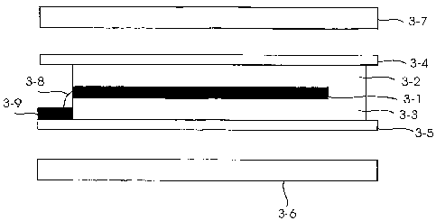
Figure 3 illustrates an antenna structure according to the invention
and its embodiments;
Figure 4 illustrates an antenna structure according to the invention
and its embodiments;
Figure 5 illustrates an antenna structure according to the invention
and its embodiments;
Figure 6A shows a subscriber identity module according to the in-
vention and its embodiments;
Figure 6B shows a cross section view of the subscriber identity
module according to the invention and its embodiments;
Figure 7 shows a non-radiating resonator antenna according to the
invention and its embodiments; and
Figure 8 shows a non-radiating resonator antenna according to the
invention and its embodiments.
Detailed description of the invention

CA 02626582 2008-04-18
WO 2007/045725 PCT/F12006/050448
3
According to the mirror image principle of the antenna theory, the
antenna should be 1/4 wavelength (in case of the GPS frequency of 1.575GHz
about 47.6 mm) distance away from a metal or a conducting ground level or
other metal part(s) to be efficient.
In one embodiment, by adding carefully measured dielectric material
layers on both sides of an antenna element, the element can be distanced
electronically from the metal parts, thus making the antenna efficient without
extending its physical dimensions, especially its thickness.
The mobile device of the invention and its embodiments can be any
mobile device like 2G (Generation), 2.5G, 3G or 4G mobile device. It can be
e.g. a mobile station, a cellular mobile station, a communicator or a
computer.
The detailed structure and operation of the mobile device and the communica-
tions systems are not relevant to the invention, and therefore they are de-
scribed only to the extent that helps understanding the invention.
Furthermore,
it should be noted that the invention can be applied to different kind of
position-
ing systems and satellite systems and to different kind of communications sys-
tems and networks like fixed networks and packet switched networks or com-
bination thereof and/or to wireless data transmission networks, such as Mobile-
f P(Intemet Protocol) networks and user equipment thereof.
For the invention and its embodiments a SIM (Subscriber Identity
Module) card can be defined to be a card removably insertable into the user
equipment containing data for subscriber identification and/or encipherment of
radio communication and/or other security related information. However, it is
to
be noted that the SIM card according to the invention and its embodiments can
but does not have be able to identify the subscriber. The card can be e.g. a
SIM card or a USIM (Universal Subscriber Identity Module) card. The structure,
the size, the physical dimensions, the weight and the layout of the card can
be
as described as follows, but they can also different ones.
A processor in the SIM card or working with the SIM card can con-
trol the access to a memory of the SIM card or to a memory working with the
SIM card used for the location of the user device e.g. in response to the iden-
tity of the location request initiator. The controf can mean e.g. the
prevention of
a location initiator from getting to the information of the memory. This means
that in one way of using the SIM card there is no direct access to the memory
of the SIM card although there can be one. The SIM card can also recognize
the location initiator being authorized to get the information directly from
the

CA 02626582 2008-04-18
WO 2007/045725 PCT/F12006/050448
4
memory of the SIM card without any authorization requests for locating the
user equipment. It is also possible that the user has given for some or all
per
sons and/or authorities preauthorization for the direct access to the memory.
The SIM card can also be a so-called tamper-proofed device offer-
ing enough protection in relation to the location of a single person.
The SIM card can also be adapted to fit to different kinds of user
equipment, to different kinds of mobile devices such that when inserted e.g.
into a conventional cellular mobile station it can adapt to the system of the
conventional mobile station and cause it to operate for locating the mobile
sta-
tion.
The SIM card can also comprise and/or be in cooperation with
logic(s) and/or software program(s) or application(s), which can control the
op-
eration of the invention and its embodiments. The logic(s), the program(s)
and/or the application(s) can be in the SIM card, in communication with the
SIM card and/or it/they can be loaded to the SIM card and/or to the user
equipment for carrying out the invention and its embodiments. The applications
comprise e.g. Java and Symbian applications.
In other words, the SIM card can comprise means e.g. a program,
for calculating the current location, like the coordinates, of the user
equipment.
2o Thus the whole processing of the positioning data and/or the current
location
can be done with the GPS chip and the SIM processor. The processor(s) of the
user equipment are not needed in the calculation but itlthey can also be used.
The SIM card can also comprise means e.g. a program, for sending
the temporary data, pseudo data to the server for the calculation of the
current
location of the user equipment.
The Java and Symbian applications can process the location infor-
mation received from the SIM card and/or from the server in many ways. The
Java application can get the location information over the GPRS (General
Packet Radio Service) network via the MSLC (Mobile Serving Location Center)
server.
The SIM card can be virtual or separate, stand-alone card. For the
invention and its embodiments the SIM card can be partly or wholly fixed to
the
user equipment or partly or wholly removably insertable into the user equip-
ment. It can thus comprise one or more parts. The SIM card can also have dif-
ferent sizes, thicknesses and volumes. Although in the following the name SIM
card will be used, it is to be understood that it also refers to different
kind of

CA 02626582 2008-04-18
WO 2007/045725 PCT/F12006/050448
smart cards like to an ICC card (Integrated Circuit Card) or to a chip card.
What is important for the invention and its embodiments is that it is a module
with embedded information receiver andlor antenna.
The antenna element and other functional blocks can receive infor-
5 mation for locating or for assisting the locationing of the equipment. Thus
they
can be in communication with e.g. a GPS (Global Positioning System) or an
AGPS (Assisted GPS) system or other satellite-positioning systems like
NAVSTAR (NAVigation System using Timing And Ranging), GLONAS (Global
Navigation Satellite Service) or GALILEO. It must be noted that the module
can comprise one or more receivers andlor antennas each of which is adapted
to e.g. different positioning systems andlor frequencies.
In other words, the accurate location of a mobile device can be de-
tected by using a satellite positioning system, such as GPS or other radio re-
ceiver or transmitter. The GPS receiver can be embedded in a SIM card.
The antenna, antenna element can be within the module or it can be
provided as a separate component. Also the antenna andlor a ground of the
user device can be used. If then the receiver unit is in the module, the
sensitiv-
ity of the system can be increased compared to the situation where both the
receiver and the antenna are in the module. This however can require the use
of new user device.
The invention and its embodiments are based on the idea of adding
a high accuracy satellite positioning system, like GPS, functionality to the
exist-
ing non-satellite positioning system, like non-GPS, user equipment without any
modifications to the device itself but only by inserting a new positioning
system
module, like AGPS enabled SIM card in it. It is also possible to insert the
high
accuracy satellite positioning system functionality to the existing satellite
posi-
tioning system user equipment.
It is possible that the user can locate his/hers position by his/hers
own initiative or the user can be located by the initiative of a third person
or a
service. However, before the third person or an external service can locate
the
user equipment, it is possible for the user to accept or reject the extemal
posi-
tioning initiative unless it is generated by emergency services with an
authority
to do so by law, or by an application or service, which is authorised by the
user. In these cases the remote location request sender can be authenticated
by a positioning application, like the AGPS application on the SIM card prior
to
requesting a positioning subsystem, like the AGPS subsystem to generate the

CA 02626582 2008-04-18
WO 2007/045725 PCT/F12006/050448
6
location data. The authentication can use digital signature (PKI) or other
avail-
able secure authentication methods to control the access to the AGPS subsys-
tem functionality. The authentication can also be used for controlling the ac-
cessing to the location information for applications running on the SIM or mo-
bile device.
The SIM module can also comprise means for controlling the ac-
cess to the positing data. When an inquiry for positioning data is received,
said
means can check the right to use andlor the right to get said positioning data
based on e.g. the identity of the sender of the inquiry. The SIM module can
transmit the positioning data or deny its transmission. The SIM module can
also calculate the location and transmit e.g. the coordinates to the initiator
of
the inquiry. The SIM card can also ask the user of the user device for the ac-
ceptance of the transmission of said data.
Figure 1 shows a cross section view, a side view of a mobile device
1-1. It comprises of a ground plane 1-2 of the mobile device, which plane can
be e.g. a metallic layer, plane or wire with different sizes and shapes in the
de-
vice andlor in the circuit board to be attached to the mobile device. It com-
prises an antenna 1-5 of the mobile device, and a battery 1-3. The Figure 1
also shows an element 1-4 according to the invention and its embodiments.
2o The element 1-4 can be e.g. the SIM card, and it can be used for receiving
RF
signals from different positioning systems like from the satellite positioning
sys-
tem for determining positioning data at least partly in response to said
signals.
The element can comprise RF receiverltransmitter that can be embedded in a
SIM card and/or in a USIM card (Universal Subscriber Identity Module). As
shown in the Figure 1, the element, subscriber module(s) is typically inserted
in
the mobile device in proximity of the ground plane 1-2 and potentially covered
by a battery 1-3.
The device chassis consists typically on printed circuit board (PCB),
electronics and a metal ground plane. The structure and measures can vary
depending on the device model. The SIM card including the antenna and being
0.76 mm think, may be located in close proximity (-1 mm) of the ground plane
and other parts containing metal, like battery.
Figure 2A shows the element 1-4 of Figure 1 and it is named as a
subscriber identity module, the SIM card, although, as stated above, it can
also
be another type of a card, a circuit board, electronics andlor software that
can
receive data from a positioning system andlor process said data for determin-

CA 02626582 2008-04-18
WO 2007/045725 PCT/F12006/050448
7
ing positioning data and/or conveying positioning data. The element 2-1 can
comprise of one or more modules, which can be separate modules or inte-
grated modules and which modules can process one or more independent or
interrelated functions. The element 2-1 comprises one or more contacts 2-2
and an RF receiver/transmitter, transceiver element 2-3. The element 2-3 can
be a circuit board with functions for receiving and/or transmifting signals.
The
element 2-3 can handle different types of signals, like RF (Radio Frequency)
signals, IF (intem7ediate Frequency) signals and baseband signals e.g. to and
from wireless transmissions, wireline transmissions and local area network.
lo One or more antenna elements are denoted as 2-5 and the element, which can
adapt to different frequencies is denoted as 2-4. This adapting means can
comprise one or more dielectric layers. One or more dielectric layers 2-4 can
surround the antenna element 2-5 wholly or partly. The layers can be such im-
plemented that on one side of the antenna element is arranged a first
dielectric
layer and on another side of the antenna element is arranged a second dielec-
tric layer. The dielectric layers can also be on top of each other. The first
di-
electric layer and/or the second dielectric layer can also be in contact with
an-
other dielectric material, with conducting material, with (semi)insulating
mate-
rial or other material with certain electromagnetic properties. The antenna 2-
10
can comprise antenna elements 2-5 and adapting means 2-4. The receiving
means can be adapted to receive the signal from a satellite positioning
system.
At least one of the dielectric layers can be adapted to the frequency of the
sig-
nal.
The ground layer of the RF transceiver relative to the antenna can
be connected to the electrical ground contact of a subscriber identity module.
Figure 2B shows a cross section view of the module according to
Figure 2A.
Figure 3 illustrates an antenna and the adapting means according to
the invention and its embodiments. The structure can be named as a Symmet-
ric Dielectric SIM Antenna. The structure can comprise of three layers: a bot-
tom dielectric layer 3-3, one or more antenna elements 3-1 and a top
dielectric
layer 3-2. Both the bottom dielectric layer and the top dielectric layer can
be
made of a thin ceramic or other material with high dielectric constant and/or
low dielectric loss. The dielectric layers can be made of same material or of
dif-
ferent materials. The thicknesses of the dielectric layers can be so designed
that they equal to 1/4 of the RF signal wavelength in the used dielectric mate-

CA 02626582 2008-04-18
WO 2007/045725 PCT/F12006/050448
8
rial, thus maximizing the signal gain. The structure 3-1, 3-2, 3-3 does not
have
form, build metallic or other ground plane, but it can alternatively use the
ground plane 3-6 of the mobile device as its own ground plane.
As a result, the structure, the antenna can be electronically large in
volume but physically thin and small in volume, and fulfilling the desired 1/4
wavelength distance frnm the metal parts for maximum gain. However, the di-
electric loss of the used material(s) 3-2 and 3-3 and small physical size of
the
antenna can cause some reduction of the performance of the antenna. The an-
tenna element can be fed 3-8 to the circuit board 3-9. The baftery 3-7 can
1 o cover the structure.
The structure of the antenna can be e.g. a monopole, a dipole, an
inverted-F, a PIFA, a fractal, a ceramic chip and a patch antenna providing
dif-
ferent radiation patterns and developed for and used with mobile devices.
Also one or more layer of plastic 3-4, 3-5 can cover said structure.
The plastic covering can be e.g. for packaging purposes and against wear.
The antenna and the RF transceiver can be integrated on the same
substrate of an integrated circuit or a circuit board or they can be separate
in-
tegrated circuits or components.
Figure 4 illustrates an antenna and the adapting means according to
the invention and its embodiments. The antenna element 4-1 and the circuit
board 4-9 can be one integral structure 4-8. The antenna element can have
the same length 4-10 within the dielectric material as the dielectric material
4-11. Alternatively the length of the antenna element can be longer or shorter
than the length of the dielectric material. The antenna element can be sur-
rounded by dielectric layer(s) 4-2, 4-3 and the whole structure can be covered
by thin layer of plastic, 4-4, 4-5. The subscriber identity module can be
covered
at least partially by at least one layer of plastic possibly excluding the
contacts.
The ground plane 4-6 can be the ground plane of the device or a
plane attached to the card.
Figure 5 illustrates an antenna 5-1 and the adapting means 5-2, 5-3
according to the invention and its embodiments. It can be named as an Asym-
metric Dielectric SIM Antenna. The structure has been adjusted such that the
top layer thickness and the bottom layer thickness of dielectric material are
dif-
ferent. The adjustment can be e.g. such that either the top layer thickness or
the bottom layer thickness is exactly or approximately 2 times thicker than
the
other layer. The thicker layer can be e.g. '/ of the wavelength in the
dielectric

CA 02626582 2008-04-18
WO 2007/045725 PCT/F12006/050448
9
material while the thickness of the other layer remains as '/ wavelength.
Based on the mirror image principle, this arrangement can substantially cancel
the RF radiation or reflections from one side of the antenna and make it im-
mune of near by metal parts on that side.
This structure can also be surrounded by plastic layers 5-4, 5-5. The
Figure also shows the baitery 5-7 and the ground plane 5-6.
Instead of a wire antenna element, a dielectric resonator and/or a
non-radiating resonator can be used to detect and receive the RF signal(s).
The resonator element can comprise a metallic layer, a plane 6-5. Figure 6
shows said subscriber identity module and a cross section view of the module.
The module 6-1 comprises of one or more contacts 6-2 and a RF re-
ceiver/transmitter element 6-3. The module also comprises of dielectric
layer(s)
6-4, a ground plane 6-6 and one or more contacts 6-7 from the SIM card to the
ground plane. By this structure a capacitive element can be implemented be-
tween the dielectric layer(s) and the ground plane. The antenna of Figure 6
can be named as a Non-radiating Resonator as a SIM antenna.
In this embodiment a resonator element 6-5 is used in the antenna
elements and/or in the SIM card in conjunction with the mobile devices ground
plane 6-6 and chassis, which can act as the other element of the resonator.
The resonator element in the SIM card can be capacitive, inductive or dielec-
tric. The connection to the resonator element in the SIM card can easily be ar-
ranged internally and the connection to the other element, i.e. the mobile de-
vice ground plane 6-6 via one or more SIM card contacts 6-2, 6-7.
The resonator element in the SIM card can form together with the
mobile device ground layer a resonator with sufficiently broad bandwidth to
work with mobile device models with different sizes of ground plates and when
located in different places in the phone.
The resonator element can form the capacitive or the inductive cou-
pling with the ground plane of the mobile device utilizing an electromagnetic
field 6-8 in between them. However, the distance 6-9 between the resonator
(the SIM card) and the ground plane may vary depending on the model and
mechanical structure of the used mobile device. The values of the distance are
typically about 0.5 mm - 5 mm. The distance 6-9 between the capacitive ele-
ments are affecting to the capacitance and consequently the impedance, the
bandwidth and the tuning frequency. To decrease the detuning effect there can
be arranged dielectric layers 6-4 on both sides of the resonant element in the

CA 02626582 2008-04-18
WO 2007/045725 PCT/F12006/050448
SIM card. In addition, by selecting material vvith high dielectric constant,
the ef-
fect of the variation of the distance between the SIM card and the ground
plane on the resonator performance can be reduced to acceptable level. In
other words, the second metal layer can be arranged to the SIM card, to the
5 mobile device and/or to the circuit board to be attached to the mobile
device.
The resonator can also be without coupling with the ground plane. It
can be for example a simple resonator circuit (RLC) connected in between the
antenna input of the receiver and the ground of the SIM card and/or a filter
to
isolate the receiver subsystem (including SIM processor) from the RF fre-
10 quency currents in the ground plane of the mobile device.
Figures 7 and 8 show a non-radiating resonator antenna according
to the invention and its embodiments. The non-radiating resonator antenna
can comprise a resonator circuit 7-4 tuned according to the receiver 7-6 fre-
quency within the bandwidth of the receiver, connected to the receiver antenna
input 7-5 and to the ground of the mobile device 7-1, which can be connected
via the SIM contacts 2-2, 8-7 to the mobile device's ground plane 1-2, 8-6.
The
resonator circuit can be e.g. an LC oscillator. The resonator circuit can also
be
implemented as a filtering means, e.g. band pass filter. The grounds of the re-
ceiver and other circuits in the SIM card can be connected to the filtered
ground, the SIM card ground 7-3, which can be connected to the ground 7-1
via the filter 7-2, which can allow DC current to pass, but is tuned to filter
at
least the frequency range of the receiver 7-6. A second or an alternative
filter
7-2 can be implemented to filter the SIM Supply Voltage 7-8. The input/output
(I/O) contact of the SIM card is shown by 7-7. 7-10 shows other possibly
blocks to be used e.g. for processing purposes. The ground 7-3 can also be
called as a virtual ground.
In other words, one or more filters 7-2 can be used to separate
those frequencies coming from the ground plate so that the frequency of inter-
est is passed trough to the receiver input. For DC and low frequency return
currents there can be a low pass filter in order to have noise free operation
of
the SIM card. The filter 7-2 can thus pass low frequencies and DC voltage, but
it can block the RF signal.
In Figure 7 the only antenna plate can be the ground layer of the
mobile device and the resonator can sense the signal from that layer.
In this arrangement the RF signal radiation 8-1 can cause high fre-
quency currents and subsequent voltages 8-2 into the ground plane 1-2, 8-6 of

CA 02626582 2008-04-18
WO 2007/045725 PCT/F12006/050448
'I 1
the mobile device, which can be connected to the ground 7-1 of the mobile de-
vice via the SIM contacts 2-2, 8-7. The ground 7-1 can thus by said to be
noisy
containing various radio frequency components. The filter 7-2 can remove high
frequency component and passes the DC current to the clean filtered ground
7-3. The difference of the noisy ground 7-1 and clean filtered ground 7-3 can
contain the received signal, which is passed to the receiver antenna input 7-5
via the resonator 7-4. The places of the filter 7-2 and the resonator 7-4 can
be
changed.
The resonator 7-4 can be implemented in several ways. It can com-
lo prise e.g. one or more of a dielectric component and/or one or more of a
resis-
tor and/or one or more of a capacitor and/or one or more of an inductor.
Also the filtering means 7-2 can be implemented in several ways. It
can comprise one or more of a dielectric component and/or one or more of a
resistor and/or one or more of a capacitor and/or one or more of an inductor
and/or one or more of a transconductor. It can be active or passive, digital
or
analog, symmetric or asymmetric and be implemented by many different tech-
niques, like gm-C technique.
The resonator, the receiving means and the filtering means can be
implemented by one or more functional blocks.
The SIM card is represented by 8-3, the circuit board of the mobile
device is represented by 8-4, the connection of mobile device ground plane 8-2
to the circuit board 8-4 is represented by 8-5 and the ground plane of the mo-
bile device is represented by 8-6.
The antenna or the antenna arrangement according to the invention
and its embodiments can be implemented in several ways. The first and the
second metal layers can alternatively or in addition be conductive or semi con-
ductive layers of other materials than metal, e.g. of plastic. The ground
level of
the SIM card can be connected to the ground level of the mobile device. The
antenna can comprise a first metal plane which is at least partly between the
first dielectric layer and/or the second dielectric layer, the first metal
plane layer
being adapted to be coupled with a second metal plane layer of the subscriber
identity module and/or the mobile device whereby a resonator is formed be-
tween the first metal layer (6-5) and the second metal layer. When the metal
layer of the mobile device is used, the resonator is formed when the antenna
arrangement is installed in the mobile device.

CA 02626582 2008-04-18
WO 2007/045725 PCT/F12006/050448
12
The antenna can be manufactured in several ways. For example, it
can be made as an ceramic component with the antenna element(s) built-in (3)
using a LTCC method, or as (flexible) Printed Circuit Board (PCB) (4) with ce-
ramic layers attached on both sides of it. Alternatively, the dielectric
material
can be sputtered on the surface of a ceramic chip antenna.
According to the invention and its embodiments many different
types of dielectric materials can be used. These materials comprise e.g.
SrTiO3 and BaxSri-xTiO3. The materials can have very high dielectric constant
(Er -300 or even more) and low dielectric loss.
If the dielectric material, such as SrTiO3 with dielectric constant Er -
300, is used for layers 3-2, 4-2 and 3-3, 4-3, the electromagnetic wavelength
in
this material is substantially 1/300 of the wavelength in free space. As an ex-
ample, GPS L9 system can use the frequency of 1.575 GHz with free space
wavelength about 190 mm. In said dielectric material the wavelength is 11300 x
190 mm = 0.633 mm and 1/4 wavelength is 0.158 mm, respectively.
The invention and its embodiments have many advantages. It is
cost efficient and easy to manufacture enabling thus the use of the GPS re-
ceiver in circumstances where traditional antennas would not work.
It will be obvious to a person skilled in the art that, as the technology
advances, the inventive concept can be implemented in various ways. The in-
vention and its embodiments are not limited to the examples described above
but may vary within the scope of the claims.

Representative Drawing
A single figure which represents the drawing illustrating the invention.
Administrative Status

2024-08-01:As part of the Next Generation Patents (NGP) transition, the Canadian Patents Database (CPD) now contains a more detailed Event History, which replicates the Event Log of our new back-office solution.

Please note that "Inactive:" events refers to events no longer in use in our new back-office solution.

For a clearer understanding of the status of the application/patent presented on this page, the site Disclaimer , as well as the definitions for Patent , Event History , Maintenance Fee  and Payment History  should be consulted.

Event History

Description Date
Time Limit for Reversal Expired 2012-10-18
Application Not Reinstated by Deadline 2012-10-18
Deemed Abandoned - Failure to Respond to Maintenance Fee Notice 2011-10-18
Letter Sent 2010-09-20
Request for Examination Requirements Determined Compliant 2010-09-07
All Requirements for Examination Determined Compliant 2010-09-07
Request for Examination Received 2010-09-07
Inactive: Office letter 2009-09-08
Inactive: Office letter 2009-08-25
Letter Sent 2009-08-25
Inactive: Single transfer 2009-07-14
Inactive: Cover page published 2008-08-21
Inactive: Notice - National entry - No RFE 2008-08-19
Inactive: First IPC assigned 2008-05-09
Application Received - PCT 2008-05-08
Inactive: Declaration of entitlement - Formalities 2008-04-30
National Entry Requirements Determined Compliant 2008-04-18
Application Published (Open to Public Inspection) 2007-04-26

Abandonment History

Abandonment Date Reason Reinstatement Date
2011-10-18

Maintenance Fee

The last payment was received on 2010-10-05

Note : If the full payment has not been received on or before the date indicated, a further fee may be required which may be one of the following

  • the reinstatement fee;
  • the late payment fee; or
  • additional fee to reverse deemed expiry.

Please refer to the CIPO Patent Fees web page to see all current fee amounts.

Fee History

Fee Type Anniversary Year Due Date Paid Date
MF (application, 2nd anniv.) - standard 02 2008-10-20 2008-04-18
Basic national fee - standard 2008-04-18
Registration of a document 2009-07-14
MF (application, 3rd anniv.) - standard 03 2009-10-19 2009-10-08
Request for examination - standard 2010-09-07
MF (application, 4th anniv.) - standard 04 2010-10-18 2010-10-05
Owners on Record

Note: Records showing the ownership history in alphabetical order.

Current Owners on Record
BLUESKY POSITIONING IPCO S.A.R.L.
Past Owners on Record
RISTO KALEVI SAVOLAINEN
Past Owners that do not appear in the "Owners on Record" listing will appear in other documentation within the application.
Documents

To view selected files, please enter reCAPTCHA code :


To view images, click a link in the Document Description column. To download the documents, select one or more checkboxes in the first column and then click the "Download Selected in PDF format (Zip Archive)" or the "Download Selected as Single PDF" button.

List of published and non-published patent-specific documents on the CPD .

If you have any difficulty accessing content, you can call the Client Service Centre at 1-866-997-1936 or send them an e-mail at CIPO Client Service Centre.


Document
Description 
Date
(yyyy-mm-dd) 
Number of pages   Size of Image (KB) 
Claims 2008-04-18 5 217
Drawings 2008-04-18 5 70
Abstract 2008-04-18 1 58
Description 2008-04-18 12 657
Representative drawing 2008-08-20 1 4
Cover Page 2008-08-21 1 34
Notice of National Entry 2008-08-19 1 194
Courtesy - Certificate of registration (related document(s)) 2009-08-25 1 121
Courtesy - Certificate of registration (related document(s)) 2009-08-25 1 102
Acknowledgement of Request for Examination 2010-09-20 1 177
Courtesy - Abandonment Letter (Maintenance Fee) 2011-12-13 1 173
PCT 2008-04-18 5 190
PCT 2008-05-13 1 47
Correspondence 2008-04-30 2 74
Correspondence 2009-08-25 1 18
Correspondence 2009-09-08 1 16