Note: Descriptions are shown in the official language in which they were submitted.
CA 02627064 2009-03-06
MULTIPLEXING VIDEO USING A DSP
TECHNICAL FIELD
[0001] The invention is related to the field of video processing.
TECHNICAL BACKGROUND
[0002] Video processing consumes large amounts of compute resources.
Because each image, or frame, of a video is a large multi-dimensional array,
and a
new image or field may arrive every 1/60t' of a second (or faster), large
volumes of
data are involved in video processing. An even larger volume of data is
processed
when a video processing system manipulates multiple video streams
simultaneously.
Because of the large volumes of data, custom and semi-custom integrated
circuits are
often used to process video.
SUMMARY
[0003] A method of operating a video processing system is disclosed. A
plurality of video streams, each comprising a sequence of frames, that were
produced
by a plurality of video Analog to Digital Converters (ADCs) are received into
a
Digital Signal Processor (DSP). The plurality of video streams are multiplexed
frame
by frame in the DSP into an unencoded multiplexed video stream. The unencoded
multiplexed video stream is transferred from the DSP to a video encoder.
[0003.1] According to another aspect of the present invention there is
provided
a video processing system, comprising: a plurality of video Analog to Digital
Converters (ADCs) converting a plurality of analog video signals into a
plurality of
digital video streams, wherein each video stream of said plurality of digital
video
1
CA 02627064 2009-03-06
streams comprises a sequence of frames; a Digital Signal Processor (DSP) that
receives said plurality of digital video streams and frame by frame generates
a
multiplexed video stream from said plurality of digital video streams; wherein
said
DSP communicates the multiplexed video stream to a video encoder in an
unencoded
format.
la
CA 02627064 2008-04-30
BRIEF DESCRIPTION OF THE DRAWINGS
[0004] Many aspects of the disclosure can be better understood with
reference to the following drawings. The components in the drawings are not
necessarily to scale, emphasis instead being placed upon clearly illustrating
the
principles of the present disclosure. Moreover, in the drawings, like
reference
numerals designate corresponding parts throughout the several views. While
several
embodiments are described in connection with these drawings, there is no
intent to
limit the disclosure to the embodiment or embodiments disclosed herein. On the
contrary, the intent is to cover all alternatives, modifications, and
equivalents.
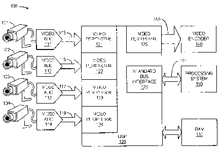
[0005] Figure 1 is a block diagram illustrating a video multiplexing system.
[0006] Figure 2 is a flowchart illustrating a method of multiplexing videos.
[0007] Figure 3 is a flowchart illustrating a method of receiving,
transferring,
and multiplexing videos.
[0008] Figure 4 is a block diagram illustrating a computer system.
DETAILED DESCRIPTION
[0009] Figures 1-4 and the following description depict specific embodiments
of the invention to teach those skilled in the art how to make and use the
best mode of
the invention. For the purpose of teaching inventive principles, some
conventional
aspects have been simplified or omitted. Those skilled in the art will
appreciate
variations from these embodiments that fall within the scope of the invention.
Those
skilled in the art will appreciate that the features described below can be
combined in
2
CA 02627064 2008-04-30
various ways to form multiple embodiments of the invention. As a result, the
invention is not limited to the specific embodiments described below, but only
by the
claims and their equivalents.
100101 Figure 1 is a block diagram illustrating a video multiplexing system.
In
Figure 1, video multiplexing system 100 comprises: analog video sources 101-
104;
video ADCs 111-114; video data streams 115-118; DSP 120; Random Access
Memory (RAM) 130; video encoder 140; processing system 150; video bus 160;
and,
standard bus 161. DSP 120 includes video peripherals 121-125 and standard bus
interface 126.
[0011] Standard bus 161 may be a Peripheral Component Interconnect (PCI) or
other parallel-specified bus. Accordingly, standard bus interface 126 may be
configured to comply with the standard specifying standard bus 161. In another
example, standard bus 161 may be a Universal Serial Bus (USB) or other serial
format specified bus.
[0012] DSP 120 may be a TMS320DM647 or TMS320DM648 digital media
processor available from Texas InstrumentsTM that may be configured to receive
multiple video data streams 115-118. Video encoder 140 may be an MG3500
available from MobilygenTM. Processing system 150 may be a computer system
based on the PowerPCTM microprocessor architecture available from
International
Business Machines (IBM).
[0013) Analog video source 101 is operatively coupled to video ADC 111.
Video ADC 11 I is operatively coupled to video peripheral 121. Analog video
source
102 is operatively coupled to video ADC 112. Video ADC 112 is operatively
coupled
to video peripheral 122. Analog video source 103 is operatively coupled to
video
3
CA 02627064 2008-04-30
ADC 113. Video ADC 113 is operatively coupled to video peripheral 123. Analog
video source 104 is operativelv coupled to video ADC 114. Video ADC 114 is
operatively coupled to video peripheral 124. Video peripherals 121-124 receive
video
data streams 115-118 from video ADCs 111-114, respectively.
[0014] Video peripheral 125 is operatively coupled to video encoder 140 via
video bus 160. Standard bus interface 126 is operatively coupled to processing
system 150 via standard bus 161. RAM 130 is operatively coupled to DSP 120.
Thus, because video peripherals 121-125 and standard bus interface 126 are all
part of
DSP 120, video peripherals 121-125 and standard bus interface 126 are all
operatively
coupled to RAM 130, video encoder 140, and processing system 150.
[0015] Analog video sources 101-104 each produce an analog video signal.
These analog video signals are converted to a digital format by video ADCs 111-
114.
The analog video signal produced by analog video source 101 is converted to a
digital
format by video ADC I 11. The analog video signal produced by analog video
source
102 is converted to a digital format by video ADC 112, and so on.
[0016] In an example, the digital format produced by ADCs 111-114 may be
specified by the International Telecommunication Union Radioconununication
Sector
(ITU-R) BT.656. A BT.656 digital video data stream is a sequence of 8-bit or
10-bit
bytes, typically transmitted at a rate of 27 Mbyte/s. The BT.656 video data
streams
115-118 produced by ADCs 111-114 are received by video peripherals 121-124,
respectively. To receive video data streams 115-118, the interfaces of video
peripherals 121-124 may be clocked at 27 MHz to match the BT.656 data rate.
[0017] DSP 120 processes and stores data from video data streams 115-118 in
RAM 130. In an example, DSP 120 processes data from video data streams 115-118
4
CA 02627064 2008-04-30
by removing blanking data from video data streams 115-118 before storing in
RAM
130. In another example, DSP 120 processes data from video data streams 115-
118
by storing each video data stream 115-118 in a different area of RAM 130.
[0018] DSP 120 alternately transfers an unencoded frame each of video data
streams 115-118 from RAM 130 to video peripheral 125. In other words, one
unencoded frame of video data stream 115 is transferred from RAM 130 to video
peripheral 125. Then, one unencoded frame of video data stream 116 is
transferred
from RAM 130 to video peripheral 125, and so on for frames of video streams
117
and 118. After a frame of video data stream 118 is transferred from RAM 130 to
video peripheral 125, the process starts again by transferring the next frame
of video
data stream 116. In this manner, video peripheral 125 receives an unencoded
multiplexed video data stream comprised of an alternating sequence of the
frames
from video data streams 115-118. In another embodiment, DSP 120 alternately
transfers an unencoded field of each frame of video data streams 115-118 from
RAM
130 to video peripheral 125.
[0019] In another embodiment, DSP 120 alternately transfers one or more
unencoded lines of a frame each of video data streams 115-118 from RAM 130 to
video peripheral 125. In other words, one or more unencoded lines of a frame
of
video data stream 115 is transferred from RAM 130 to video peripheral 125.
Then,
one or more unencoded lines of a frame of video data stream 116 is transferred
from
RAM 130 to video peripheral 125, and so on for lines of video data streams 117
and
118. After the line or lines of video data stream 118 is transferred from RAM
130 to
video peripheral 125, the process starts again by transferring the next line
or lines of
video data stream 116. In this manner, video peripheral 125 receives an
unencoded
CA 02627064 2008-04-30
multiplexed video data stream comprised of an alternating sequence of lines
from
video data streams 115-118. In an embodiment, the line or lines of the video
data
streams each 115-118 comprise a field of an interlaced frame.
100201 Video peripheral 125 transfers the unencoded multiplexed video data
stream to video encoder 140 via video bus 160. In an example, video peripheral
125
transfers the unencoded multiplexed video data stream to video encoder 140 in
BT.656 format at a rate of 108 Mbytes/s. To transfer the unencoded multiplexed
video data stream at that rate, the interface of video peripheral 125 may be
clocked at
108 MHz to match the data rate.
[0021) DSP 120 may also encode or otherwise process one or more of video
data streams 115-118 while they are stored in RAM 130. DSP 120 may encode one
or more of video data streams 115-118 and store the encoded version in RAM
130.
For example, video data stream 115-118 may be encoded or compressed into a
Moving Picture Experts Group (MPEG) specified format such as MPEG-4.
100221 In another example, DSP 120 processes one or more of video data
streams 115-118 to perform video analytics. Video Analytics is a technology
that is
used to analyze video for specific data, behavior, objects or attitude.
Examples of
video analytics applications include: counting the number of pedestrians
entering a
door or geographic region, determining the location, speed and direction of
travel,
identifying suspicious movement of people or assets, license plate
identification, face
recognition, or evaluating how long a package has been left in an area.
[0023] DSP 120 may transfer an encoded version of video data stream 115-118
to processing system 150 via standard bus interface 126 and standard bus 161.
DSP
6
CA 02627064 2008-04-30
120 may also transfer other information, such as the results of video
analytics, to
processing system 150 standard bus interface 126 and standard bus 161.
[0024] Figure 2 is a flowchart illustrating a method of multiplexing videos.
The method of Figure 2 may be performed by video multiplexing system 100.
Multiple analog videos are digitized in parallel into multiple digital video
streams
(202). These digital video streams are received in a DSP (204).
[0025] The multiple digital video streams received in the DSP are multiplexed
in the DSP into an unencoded multiplexed video stream (206). For example, DSP
120
may alternately transfer an unencoded frame each of video data streams 115-118
from
RAM 130 to video peripheral 125. In other words, one unencoded frame of video
data stream 115 may be transferred from RAM 130 to video peripheral 125. Then,
one unencoded frame of video data stream 116 may be transferred from RAM 130
to
video peripheral 125, and so on for frames of video data streams 117 and 118.
After a
frame of video data stream 118 is transferred from RAM 130 to video peripheral
125,
the process may start again by transferring the next frame of video data
stream 116.
In this manner, an unencoded multiplexed video data stream comprised of an
alternating sequence of the frames from video data streams 115-118 is
produced.
[0026] In another example, DSP 120 may alternately transfers one or more
unencoded lines of a frame each of video data streams 115-118 from RAM 130 to
video peripheral 125. In other words, one or more unencoded lines of a frame
of
video data stream 115 may be transferred from RAM 130 to video peripheral 125.
Then, one or more unencoded lines of a frame of video data stream 116 may be
transferred from RAM 130 to video peripheral 125, and so on for lines of video
data
streams 117 and 118. After the line or lines of video data stream 118 is
transferred
7
CA 02627064 2008-04-30
from RAM 130 to video peripheral 125, the process may start again by
transferring
the next line or lines of video data stream 116. In this manner, an unencoded
multiplexed video data stream comprised of an alternating sequence of lines
from
video data streams 115-118 is produced.
[0027] The unencoded multiplexed video data stream is transferred to an
encoder (208). For example, DSP 120 may transfer the unencoded multiplexed
video
data stream to video encoder 140 via video bus 160.
[0028] A digital video data stream is encoded into a first format in the DSP
(210). For example, DSP 120 may encode one or more of video data streams 115-
118
while they are stored in RAM 130. DSP 120 may encode one or more of video data
streams 115-118 and store the encoded version in RAM 130. In an example, video
data stream 115-118 may be encoded or compressed into a format such as MPEG-4.
[0029] The encoded digital video data stream may be transferred in the first
format to a processing system (212). For example, DSP 120 may transfer an
encoded
version of video data stream 115-118 to processing system 150 via standard bus
interface 126 and standard bus 161.
[0030] Figure 3 is a flowchart illustrating a method of receiving,
transferring,
and multiplexing videos. The method of Figure 3 may be performed by video
multiplexing system 100. Multiple input video peripherals are configured to
receive
input videos at a first clock frequency. For example, video peripherals 121-
124 may
be configured to receive BT.656 formatted digital video at a clock rate of 27
MHz.
8
CA 02627064 2008-04-30
[0031] An output video peripheral is configured to send video at a second
clock frequency (304). For example, video peripheral 125 may be configured to
send
video at a clock rate of 108 MHz.
[0032] The input videos are multiplexed (306). The multiplexed video is
transferred to the output video peripheral (308). For example, DSP 120 may
alternately transfer unencoded frames that correspond to each of video data
streams
115-118 to video peripheral 125.
[0033] The methods, systems, devices, DSP, video peripherals, bus interfaces,
interfaces, processing system, video encoder, ADCs, described above may be
implemented with, contain, or be executed by one or more computer systems. The
methods described above may also be stored on a computer readable medium. Many
of the elements of video multiplexing system 100 may be, comprise, or include
computers systems. This includes, but is not limited to: analog video sources
101-
104; video ADCs 111-114; DSP 120; video encoder 140; processing system 150;
DSP
120; and, video peripherals 121-125. These computer systems are illustrated,
by way
of example, in Figure 4.
[0034] Figure 4 illustrates a block diagram of a computer system. Computer
system 400 includes communication interface 420, processing system 430, and
user
interface 460. Processing system 430 includes storage system 440. Storage
system
440 stores software 450. Processing system 430 is linked to communication
interface
420 and user interface 460. Computer system 400 could be comprised of a
programmed general-purpose computer, although those skilled in the art will
appreciate that programmable or special purpose circuitry and equipment may be
9
CA 02627064 2008-04-30
used. Computer system 400 may be distributed among multiple devices that
together
comprise elements 420-460.
[0035] Communication interface 420 could comprise a network interface,
modem, port, transceiver, or some other communication device. Communication
interface 420 may be distributed among multiple communication devices.
Processing
system 430 could comprise a computer microprocessor, logic circuit, or some
other
processing device. Processing system 430 may be distributed among multiple
processing devices. User interface 460 could comprise a keyboard, mouse, voice
recognition interface, microphone and speakers, graphical display, touch
screen, or
some other type of user device. User interface 460 may be distributed among
multiple user devices. Storage system 440 could comprise a disk, tape,
integrated
circuit, server, or some other memory device. Storage system 440 may be
distributed
among multiple memory devices.
[0036] Processing system 430 retrieves and executes software 450 from
storage system 440. Software 450 may comprise an operating system, utilities,
drivers, networking software, and other software typically loaded onto a
computer
system. Software 450 could comprise an application program, firmware, or some
other form of machine-readable processing instructions. When executed by
processing system 430, software 450 directs processing system 430 to operate
as
described herein.
[0037] The above description and associated figures teach the best mode of the
invention. The following claims specify the scope of the invention. Note that
some
aspects of the best mode may not fall within the scope of the invention as
specified by
the claims. Those skilled in the art will appreciate that the features
described above
CA 02627064 2008-04-30
can be combined in various ways to form multiple variations of the invention.
As a
result, the invention is not limited to the specific embodiments described
above, but
onlv by the following claims and their equivalents.
11