Note: Descriptions are shown in the official language in which they were submitted.
CA 02627311 2008-04-21
WO 2008/033149 PCT/US2006/041548
-1-
SEQUENTIALLY PULSED TRAVELING WAVE ACCELERATOR
[0001] The United States Government has rights in this invention pursuant to
Contract No. W-7405-ENG-48 between the United States Department of Energy
and the University of California for the operation of Lawrence Livermore
National Laboratory.
I. REFERENCE TO PRIOR APPLICATIONS
[0002] This application is a continuation-in-part of prior Application No.
11/036,431, filed January 14, 2005, which claims the benefit of Provisional
Application No. 60/536,943, filed Januaiy 15, 2004; and this application also
claims the benefit of U.S. Provisional Application Nos. 60/730,128,
60/730,129,
and 60/730,161, filed October 24, 2005, and U.S. Provisional Application No.
60/798016, filed May 4, 2006, all of which are incorporated by reference
herein.
II. = FIELD OF THE INVENTION
[0003] The present invention relates to linear accelerators and more
particularly
to a sequentially pulsed traveling wave accelerator capable of sequentially
triggering switches to differentially propagate electric wavefronts through
pulse-
forming lines of a linear accelerator to produce a traveling axial electrical
field
along a beam tube of the accelerator in synchronism with an axially traversing
pulsed beam of charged particles to serially impart energy to the particle
beam.
III. BACKGROUND OF THE INVENTION
[0004] Particle accelerators are used to increase the energy of electrically-
charged
atomic particles, e.g., electrons, protons, or charged atomic nuclei, so that
they
can be studied by nuclear and particle physicists. High energy electrically-
charged atomic particles are accelerated to collide with target atoms, and the
resulting products are observed with a detector. At very high energies the
charged
particles can break up the nuclei of the target atoms and interact with other
CA 02627311 2008-04-21
WO 2008/033149 PCT/US2006/041548
-2-
fundamental units of matter. Particle accelerators are also important tools in
the
effort to develop nuclear fusion devices, as well as for medical applications
such
as cancer therapy.
[0005] One type of particle accelerator is disclosed in U.S. Pat. No.
5,757,146 to
Carder, incorporated by reference herein, for providing a method to generate a
fast electrical pulse for the acceleration of charged particles. In Carder, a
dielectric wall accelerator (DWA) system is shown consisting of a series of
stacked circular modules which generate a high voltage when switched. Each of
these modules is called an asymmetric Blumlein, which is described in U.S.
Pat.
No. 2,465,840 incorporated by reference herein. As can be best seen in Figures
4A-4B of the Carder patent, the Blumlein is composed of two different
dielectric
layers. On each surface and between the dielectric layers are conductors which
form two parallel plate radial transmission lines. One side of the structure
is
referred to as the slow line, the other is the fast line. The center electrode
between
the fast and slow line is initially charged to a high potential. Because the
two
lines have opposite polarities there is no net voltage across the inner
diameter (ID)
of the Blumlein. Upon applying a short circuit across the outside of the
structure
by a surface flashover or similar switch, two reverse polarity waves are
initiated
which propagate radially inward towards the ID of the Blumlein. The wave in
the
fast line reaches the ID of the structure prior to the arrival of the wave in
the slow
line. When the fast wave arrives at the ID of the structure, the polarity
there is
reversed in that line only, resulting in a net voltage across the ID of the
asymmetric Blumlein. This high voltage will persist until the wave in the slow
line finally reaches the ID. In the case of an accelerator, a charged particle
beam
can be injected and accelerated during this time. In this manner, the DWA
accelerator in the Carder patent provides an axial accelerating field that
continues
over the entire structure in order to achieve high acceleration gradients.
[0006] The existing dielectric wall accelerators, such as the Carder DWA,
however, have certain inherent problems which can affect beam quality and
performance. In particular, several problems exist in the disc-shaped geometry
of
the Carder DWA which make the overall device less than optimum for the
CA 02627311 2008-04-21
WO 2008/033149 PCT/US2006/041548
-3-
intended use of accelerating charged particles. The flat planar conductor with
a
central hole forces the propagating wavefront to radially converge to that
central
hole. In such a geometry, the wavefront sees a varying iinpedance which can
distort the output pulse, and prevent a defined time dependent energy gain
from
being imparted to a charged particle beam traversing the electric field.
Instead, a
charged particle beam traversing the electric field created by such a
structure will
receive a time varying energy gain, which can prevent an accelerator system
from
properly transporting such beam, and making such beams of limited use.
[0007] Additionally, the impedance of such a structure may be far lower than
required. For instance, it is often highly desirable to generate a beam on the
order
of milliamps or less while maintaining the required acceleration gradients.
The
disc-shaped Blumlein structure of Carder can cause excessive levels of
electrical
energy to be stored in the system. Beyond the obvious electrical
inefficiencies,
any energy which is not delivered to the beam when the system is initiated can
remain in the structure. Such excess energy can have a detrimental effect on
the
performance and reliability of the overall device, which can lead to premature
failure of the system.
[0008] And inherent in a flat planar conductor with a central hole (e.g. disc-
shaped) is the greatly extended circumference of the exterior of that
electrode. As
a result, the number of parallel switches to initiate the structure is
determined by
that circumference. For example, in a 6" diameter device used for producing
less
than a I Ons pulse typically requires, at a minimum, 10 switch sites per disc-
shaped asymmetric Blumlein layer. This problem is further compounded when
long acceleration pulses are required since the output pulse length of this
disc-
shaped Blumlein structure is directly related to the radial extent from the
central
hole. Thus, as long pulse widths are required, a corresponding increase in
switch
sites is also required. As the preferred embodiment of initiating the switch
is the
use of a laser or other similar device, a highly complex distribution system
is
required. Moreover, a long pulse structure requires large dielectric sheets
for
which fabrication is difficult. This can also increase the weight of such a
structure. For instance, in the present configuration, a device delivering 50
ns
CA 02627311 2008-04-21
WO 2008/033149 PCT/US2006/041548
-4-
pulse can weigh as much as several tons per meter. While some of the long
pulse
disadvantages can be alleviated by the use of spiral grooves in all three of
the
conductors in the asymmetric Blumlein, this can result in a destructive
interference layer-to-layer coupling which can inhibit the operation. That is,
a
sigiiificantly reduced pulse amplitude (and therefore energy) per stage can
appear
on the output of the structure.
[0009] Additionally, various types of accelerators have been developed for
particular use in medical therapy applications, such as cancer therapy using
proton
beams. For example, U.S. Pat. No. 4,879,287 to Cole et al discloses a multi-
station proton beam therapy system used for the Loma Linda University Proton
Accelerator Facility in Loma Linda, California. In this system, particle
source
generation is performed at one location of the facility, acceleration is
performed at
another location of the facility, while patients are located at still other
locations of
the facility. Due to the remoteness of the source, acceleration, and target
from
each other particle transport is accomplished using a complex gantry system
with
large, bulky bending magnets. And other representative systems known for
medical therapy are disclosed in U.S. Pat. No. 6,407,505 to Bertsche and U.S.
Pat.
No. 4,507,616 to Blosser et al. In Berstche, a standing wave RF linac is shown
and in Blosser a superconducting cyclotron rotatably mounted on a support
structure is shown.
[0010] Furthermore, ion sources are known which create a plasma discharge from
a low pressure gas within a volume. From this voluine, ions are extracted and
collimated for acceleration into an accelerator. These systems are generally
limited to extracted current densities of below 0.25 A/cm2. This low current
density is partially due to the intensity of the plasma discharge at the
extraction
interface. One example of an ion source lcnown in the art is disclosed in U.S.
Pat.
No. 6,985,553 to Leung et al having an extraction system configured to produce
ultra-short ion pulses. Another example is shown in U.S. Pat. No. 6,759,807 to
Wahlin disclosing a multi-grid ion beam source having an extraction grid, an
acceleration grid, a focus grid, and a shield grid to produce a highly
collimated
ion beam.
CA 02627311 2008-04-21
WO 2008/033149 PCT/US2006/041548
-5-
IV. SUMMARY OF THE INVENTION
[0011] One aspect of the present invention includes a short pulse dielectric
wall
accelerator comprising: a dielectric beam tube of length L surrounding an
acceleration axis; at least two pulse-forming lines transversely connected to
the
beam tube, each pulse-forming line having a switch connectable to a high
voltage
potential for propagating at least one electrical wavefront(s) therethrough
independent of other pulse-forming lines to produce a short acceleration pulse
of
pulse width ti along a corresponding short axial length 8L of the beam tube;
and
means for sequentially controlling the switches so that a traveling axial
electric
field is produced along the beam tube in synchronism with an axially
traversing
pulsed beam of charged particles to serially impart energy to said particles.
[0012] Another aspect of the present invention includes a sequentially pulsed
traveling wave linear accelerator comprising: a plurality of pulse-forming
lines
extending to a transverse acceleration axis, each pulse-forming line having a
switch connectable to a high voltage potential for propagating at least one
electrical wavefront(s) therethrough independent of other pulse-forming lines
to
produce a short acceleration pulse adjacent a corresponding short axial length
of
the acceleration axis; and a trigger operably connected to sequentially
control the
switches so that a traveling axial electric field is produced along the
acceleration
axis in synchronism with an axially traversing pulsed beam of charged
particles to
serially impart energy to said particles.
[0013] Ariother aspect of the present invention includes a sequentially pulsed
traveling wave linear accelerator comprising: a dielectric beam tube of length
L
surrounding an acceleration axis; at least two Blumlein modules, each forming
a
pulse-forming line transverse to the acceleration axis and comprising: a first
conductor having a first end, and a second end connected to the beam tube; a
second conductor adjacent to the first conductor, said second conductor having
a
first end switchable to the high voltage potential, and a second end connected
to
the beam tube; a third conductor adjacent to the second conductor, said third
conductor having a first end, and a second end connected to the beam tube; a
first
CA 02627311 2008-04-21
WO 2008/033149 PCT/US2006/041548
-6-
dielectric material with a first dielectric constant that fills the space
between the
first and second conductors; and a second dielectric material with a second
dielectric constant that fills the space between the second and third
conductors,
with the first and second dielectric constants less than the dielectric
constant of
the beam tube; each Blumlein module having at least one switch connectable to
a
high voltage potential for propagating at least one electrical wavefront(s)
therethrough independent of other Blumlein modules to produce a short
acceleration pulse of pulse width i along a corresponding short axial length
8L of
the beam tube; and a controller operably connected to sequentially trigger the
switches so that a traveling axial electric field is produced along the beam
tube in
synchronism with an axially traversing pulsed beain of charged particles to
serially impart energy to said particles.
V. BRIEF DESCRIPTION OF THE DRAWINGS
[0014] The accompanying drawings, which are incorporated into and form a part
of the disclosure, are as follows:
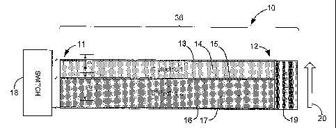
[0015] Figure 1 is a side view of a first exemplary embodiment of a single
Blumlein module of the compact accelerator of the present invention.
[0016] Figure 2 is top view of the single Blumlein module of Figure 1.
[0017] Figure 3 is a side view of a second exemplary embodiment of the compact
accelerator having two Blumlein modules stacked together.
[0018] Figure 4 is a top view of a third exemplary embodiment of a single
Blumlein module of the present invention having a middle conductor strip with
a
smaller width than other layers of the module.
[0019] Figure 5 is an enlarged cross-sectional view taken along line 4 of
Figure 4.
[0020] Figure 6 is a plan view of another exemplary embodiment of the compact
accelerator shown with two Blumlein modules perimetrically surrounding and
radially extending towards a central acceleration region.
[0021] Figure 7 is a cross-sectional view taken along line 7 of Figure 6.
[0022] Figure 8 is a plan view of another exemplary embodiment of the compact
accelerator shown with two Blumlein modules perimetrically surrounding and
CA 02627311 2008-04-21
WO 2008/033149 PCT/US2006/041548
-7-
radially extending towards a central acceleration region, with planar
conductor
strips of one module connected by ring electrodes to corresponding planar
conductor strips of the other module.
[0023] Figure 9 is a cross-sectional view taken along line 9 of Figure 8.
[0024] Figure 10 is a plan view of another exemplary embodiment of the present
invention having four non-linear Blumlein modules each connected to an
associated switch.
[0025] Figure 11 is a plan view of another exemplary embodiment of the present
invention similar to Figure 10, and including a ring electrode connecting each
of
the four non-linear Blumlein modules at respective second ends thereof.
[0026] Figure 12 is a side view of another exemplary embodiment of the present
invention similar to Figure 1, and having the first dielectric strip and the
second
dielectric strip having the same dielectric constants and the same
thicknesses, for
symmetric Blumlein operation.
[0027] Figure 13 is schematic view of an exemplary embodiment of the charged
particle generator of the present invention.
[0028] Figure 14 is an enlarged schematic view taken along circle 14 of Figure
13, showing an exemplary embodiment of the pulsed ion source of the present
invention.
[0029] Figure 15 shows a progression of pulsed ion generation by the pulsed
ion
source of Figure 14.
[0030] Figure 16 shows multiple screen shots of final spot sizes on the target
for
various gate electrode voltages.
[0031] Figure 17 shows a graph of extracted proton beam current as a function
of
the gate electrode voltage on a high-gradient proton beain accelerator.
[0032] Figure 18 shows two graphs showing potential contours in the charged
particle generator of the present invention.
[0033] Figure 19 is a comparative view of beam transport in a magnet-free 250
MeV high-gradient proton accelerator with various focus electrode voltage
settings.
CA 02627311 2008-04-21
WO 2008/033149 PCT/US2006/041548
-8-
[0034] Figure 20 is a comparative view of four graphs of the edge beam radii
(upper curves) and the core radii (lower curves) on the target versus the
focus
electrode voltage for 250 MeV, 150 MeV, 100 MeV, and 70 MeV proton beams.
[0035] Figure 21 is a schematic view of the actuable compact accelerator
system
of the present invention having an integrated unitary charged particle
generator
and linear accelerator.
[0036] Figure 22 is a side view of an exemplary mounting arrangement of the
unitary compact accelerator/charged particle source of the present invention,
illustrating a medical therapy application.
[0037] Figure 23 is a perspective view of an exemplary vertical mounting
arrangement of the unitary compact accelerator/charged particle source of the
present invention.
[0038] Figure 24 is a perspective view of an exemplary hub-spoke mounting
arrangement of the unitary compact accelerator/charged particle source of the
present invention.
[0039] Figure 25 is a schematic view of a sequentially pulsed traveling wave
accelerator of the present invention.
[0040] Figure 26 is a schematic view illustrating a short pulse traveling wave
operation of the sequentially pulsed traveling wave accelerator of Figure 25.
[0041] Figure 27 is a schematic view illustrating a long pulse operation of a
typical cell of a conventional dielectric wall accelerator.
VI. DETAILED DESCRIPTION
A. Compact Accelerator with Strip-shaped Blumlein
[0042] Turning now to the drawings, Figures 1-12 show a compact linear
accelerator used in the present invention, having at least one strip-shaped
Blumlein module which guides a propagating wavefront between first and second
ends and controls the output pulse at the second end. Each Blumlein module has
first, second, and third planar conductor strips, with a first dielectric
strip between
the first and second conductor strips, and a second dielectric strip between
the
second and third conductor strips. Additionally, the compact linear
accelerator
CA 02627311 2008-04-21
WO 2008/033149 PCT/US2006/041548
-9-
includes a high voltage power supply connected to charge the second conductor
strip to a high potential, and a switch for switching the high potential in
the
second conductor strip to at least one of the first and third conductor strips
so as to
initiate a propagating reverse polarity wavefront(s) in the corresponding
dielectric
strip(s).
[0043] The compact linear accelerator has at least one strip-shaped Blumlein
module which guides a propagating wavefront between first and second ends and
controls the output pulse at the second end. Each Blumlein module has first,
second, and third planar conductor strips, with a first dielectric strip
between the
first and second conductor strips, and a second dielectric strip between the
second
and third conductor strips. Additionally, the compact linear accelerator
includes a
high voltage power supply connected to charge the second conductor strip to a
high potential, and a switch for switching the high potential in the second
conductor strip to at least one of the first and third conductor strips so as
to initiate
a propagating reverse polarity wavefront(s) in the corresponding dielectric
strip(s).
[0044] Figures 1-2 show a first exemplary embodiment of the compact linear
accelerator, generally indicated at reference character 10, and comprising a
single
Blumlein module 36 connected to a switch 18. The compact accelerator also
includes a suitable high voltage supply (not shown) providing a high voltage
potential to the Blumlein module 36 via the switch 18. Generally, the Blumlein
module has a strip configuration, i.e. a long narrow geometry, typically of
unifonn width but not necessarily so. The particular Blumlein module 11 shown
in Figures 1 and 2 has an elongated beam or plank-like linear configuration
extending between a first end 11 and a second end 12, and having a relatively
narrow width, w7z (Figs. 2, 4) compared to the length, 1. This strip-shaped
configuration of the Blumlein module operates to guide a propagating
electrical
signal wave from the first end 11 to the second end 12, and thereby control
the
output pulse at the second end. In particular, the shape of the wavefront may
be
controlled by suitably configuring the width of the module, e.g. by tapering
the
width as shown in Figure 6. The strip-shaped configuration enables the compact
CA 02627311 2008-04-21
WO 2008/033149 PCT/US2006/041548
-10-
accelerator to overcome the varying impedance of propagating wavefronts which
can occur when radially directed to converge upon a central hole as discussed
in
the Background regarding disc-shaped module of Carder. And in this manner, a
flat output (voltage) pulse can be produced by the strip or beam-like
configuration
of the module 10 without distorting the pulse, and thereby prevent a particle
beam
from receiving a time varying energy gain. As used herein and in the claims,
the
first end 11 is characterized as that end which is connected to a switch, e.g.
switch
18, and the second end 12 is that end adjacent a load region, such as an
output
pulse region for particle acceleration.
[0045] As shown in Figures 1 and 2, the narrow beam-like structure of the
basic
Blumlein module 10 includes three planar conductors shaped into thin strips
and
separated by dielectric material also shown as elongated but thicker strips.
In
particular, a first planar conductor strip 13 and a middle second planar
conductor
strip 15 are separated by a first dielectric material 14 which fills the space
therebetween. And the second planar conductor strip 15 and a third planar
conductor strip 16 are separated by a second dielectric material 17 which
fills the
space therebetween. Preferably, the separation produced by the dielectric
materials positions the planar conductor strips 13, 15 and 16 to be parallel
with
each other as shown. A third dielectric material 19 is also shown connected to
and capping the planar conductor strips and dielectric strips 13-17. The third
dielectric material 19 serves to combine the waves and allow only a pulsed
voltage to be across the vacuum wall, thus reducing the time the stress is
applied
to that wall and enabling even higher gradients. It can also be used as a
region to
transform the wave, i.e., step up the voltage, change the impedance, etc.
prior to
applying it to the accelerator. As such, the third dielectric material 19 and
the
second end 12 generally, are shown adjacent a load region indicated by arrow
20.
In particular, arrow 20 represents an acceleration axis of a particle
accelerator and
pointing in the direction of particle acceleration. It is appreciated that the
direction of acceleration is dependent on the paths of the fast and slow
transmission lines, through the two dielectric strips, as discussed in the
Background.
CA 02627311 2008-04-21
WO 2008/033149 PCT/US2006/041548
-11-
[0046] In Figure 1, the switch 18 is shown connected to the planar conductor
strips 13, 15, and 16 at the respective first ends, i.e. at first end 11 of
the module
36. The switch serves to initially connect the outer planar conductor strips
13, 16
to a ground potential and the middle conductor strip 15 to a high voltage
source
(not shown). The switch 18 is then operated to apply a short circuit at the
first
end so as to initiate a propagating voltage wavefront through the Blumlein
module
and produce an output pulse at the second end. In particular, the switch 18
can
initiate a propagating reverse polarity wavefront in at least one of the
dielectrics
from the first end to the second end, depending on whether the Blumlein module
is configured for symmetric or asymmetric operation. When configured for
asymmetric operation, as shown in Figures 1 and 2, the Blumlein module
comprises different dielectric constants and thicknesses (dl $ d2) for the
dielectric
layers 14, 17, in a manner similar to that described in Carder. The asymmetric
operation of the Blumlein generates different propagating wave velocities
through
the dielectric layers. However, when the Blumlein module is configured for
symmetric operation as shown in Figure 12, the dielectric strips 95, 98 are of
the
same dielectric constant, and the width and thiclcness (dl = d2) are also the
same.
In addition, as shown in Figure 12, a magnetic material is also placed in
close
proximity to the second dielectric strip 98 such that propagation of the
wavefront
is inhibited in that strip. In this manner, the switch is adapted to initiate
a
propagating reverse polarity wavefront in only the first dielectric strip 95.
It is
appreciated that the switch 18 is a suitable switch for asymmetric or
symmetric
Blumlein module operation, such as for example, gas discharge closing
switches,
surface flashover closing switches, solid state switches, photoconductive
switches, etc. And it is further appreciated that the choice of switch and
dielectric
material types/dimensions can be suitably chosen to enable the compact
accelerator to operate at various acceleration gradients, including for
example
gradients in excess of twenty megavolts per meter. However, lower gradients
would also be achievable as a matter of design.
[0047] In one preferred embodiment, the second planar conductor has a width,
wl
defined by characteristic impedance ZI = kigl(wl,dl) through the first
dielectric
CA 02627311 2008-04-21
WO 2008/033149 PCT/US2006/041548
-12-
strip. kl is the first electrical constant of the first dielectric strip
defined by the
square root of the ratio of permeability to permittivity of the first
dielectric
material, gi is the function defined by the geometry effects of the
neighboring
conductors, and dl is the thickness of the first dielectric strip. And the
second
dielectric strip has a thickness defuied by characteristic impedance Z2 =
k2g2(w2,
d2) through the second dielectric strip. In this case, k2 is the second
electrical
constant of the second dielectric material, g2 is the function defined by the
geometry effects of the neighboring conductors, and w2 is the width of the
second
planar conductor strip, and d2 is the thickness of the second dielectric
strip. In
this manner, as differing dielectrics required in the asymmetric Blumlein
module
result in differing impedances, the impedance can now be hold constant by
adjusting the width of the associated line. Thus greater energy transfer to
the load
will result.
[0048] Figures 4 and 5 show an exemplary embodiment of the Blumlein module
having a second planar conductor strip 42 with a width that is narrower than
those
of the first and second planar conductor strips 41, 42, as well as first and
second
dielectric strips 44, 45. In this particular configuration, the destructive
interference layer-to-layer coupling discussed in the Background is inhibited
by
the extension of electrodes 41 and 43 as electrode 42 can no longer easily
couple
energy to the previous or subsequent Blumlein. Furthermore, another exemplary
embodiment of the module preferably has a width which varies along the
lengthwise direction, 1, (see Figures 2, 4) so as to control and shape the
output
pulse shape. This is shown in Figure 6 showing a tapering of the width as the
module extends radially inward towards the central load region. And in another
preferred embodiment, dielectric materials and dimensions of the Blumlein
module are selected such that, ZI is substantially equal to Z2. As previously
discussed, match impedances prevent the formation of waves which would create
an oscillatory output.
[0049] And preferably, in the asymmetric Blumlein configuration, the second
dielectric strip 17 has a substantially lesser propagation velocity than the
first
dielectric strip 14, such as for example 3:1, where the propagation velocities
are
CA 02627311 2008-04-21
WO 2008/033149 PCT/US2006/041548
-13-
defined by v2, and vl, respectively, where v2 ( 282)- 5 and vl =(,ulsl)- =S;
the
permeability, ,ul, and the permittivity, EI, are the material constants of the
first
dielectric material; and the permeability, ,u2, and the permittivity, aZ, are
the
material constants of the second dielectric material. This can be achieved by
selecting for the second dielectric strip a material having a dielectric
constant, i.e.
p181 , which is greater than the dielectric constant of the first dielectric
strip, i.e.
,u2E2. As shown in Figure 1, for example, the thickness of the first
dielectric strip
is indicated as dl, and the thickness of the second dielectric strip is
indicated as d2,
with d2 shown as being greater than dl. By setting d2 greater than dl, the
combination of different spacing and the different dielectric constants
results in
the same characteristic impedance, Z, on both sides of the second planar
conductor strip 15. It is notable that although the characteristic impedance
may
be the same on both halves, the propagation velocity of signals through each
half
is not necessarily the same. While the dielectric constants and the
thicknesses of
the dielectric strips may be suitably chosen to effect different propagating
velocities, it is appreciated that the elongated strip-shaped structure and
configuration need not utilize the asymmetric Blumlein concept, i.e.
dielectrics
having different dielectric constants and thicknesses. Since the controlled
waveform advantages are made possible by the elongated beam-like geometry and
configuration of the Blumlein modules, and not by the particular method of
producing the high acceleration gradient, another exemplary embodiment can
employ alternative switching arrangements, such as that discussed for Figure
12
involving symmetric Blumlein operation.
[0050] The compact accelerator may alternatively be configured to have two or
more of the elongated Blumlein modules stacked in alignment with each other.
For example, Figure 3 shows a compact accelerator 21 having two Blumlein
modules stacked together in alignment with each other. The two Blumlein
modules form an alternating stack of planar conductor strips and dielectric
strips
24-32, with the planar conductor strip 32 common to both modules. And the
conductor strips are connected at a first end 22 of the stacked module to a
switch
33. A dielectric wall is also provided at 34 capping the second end 23 of the
CA 02627311 2008-04-21
WO 2008/033149 PCT/US2006/041548
-14-
stacked module, and adjacent a load region indicated by acceleration axis
arrow
35.
[0051] The compact accelerator may also be configured with at least two
Blumlein modules which are positioned to perimetrically surround a central
load
region. Furthermore, each perimetrically surrounding module may additionally
include one ore more additional Blumlein modules stacked to align with the
first
module. Figure 6, for example, shows an exemplary embodiment of a compact
accelerator 50 having two Blumlein module stacks 51 and 53, with the two
stacks
surrounding a central load region 56. Each module stack is shown as a stack of
four independently operated Bluinlein modules (Figure 7), and is separately
coimected to associated switches 52, 54. It is appreciated that the stacking
of
Blumlein modules in alignment with each other increases the coverage of
segments along the acceleration axis.
[0052] In Figures 8 and 9 another exemplary embodiment of a compact
accelerator is shown at reference character 60, having two or more conductor
strips, e.g. 61, 63, connected at their respective second ends by a ring
electrode
indicated at 65. The ring electrode configuration operates to overcome any
azimuthal averaging which may occur in the arrangement of such as Figures 6
and
7 where one or more perimetrically surrounding modules extend towards the
central load region without completely surrounding it. As best seen in Figure
9,
each module stack represented by 61 and 62'is connected to an associated
switch
62 and 64, respectively. Furthermore, Figures 8 and 9 show an insulator sleeve
68 placed along an interior diameter of the ring electrode. Alternatively,
separate
insulator material 69 is also shown placed between the ring electrodes 65. And
as
an alternative to the dielectric material used between the conductor strips,
alternating layers of conducting 66 and insulating 66' foils may be utilized.
The
alternative layers may be formed as a laminated structure in lieu of a
monolithic
dielectric strip.
[0053] And Figures 10 and 11 show two additional exemplary embodiments of
the compact accelerator, generally indicated at reference character 70 in
Figure
10, and reference character 80 in Figure 11, each having Blumlein modules with
CA 02627311 2008-04-21
WO 2008/033149 PCT/US2006/041548
-15-
non-linear strip-shaped configurations. In this case, the non-linear strip-
shaped
configuration is shown as a curvilinear or serpentine form. In Figure 10, the
accelerator 70 comprises four modules 71, 73, 75, and 77, shown perimetrically
surrounding and extending towards a central region. Each module 71, 73, 75,
and
77, is connected to an associated switch, 72, 74, 76, and 78, respectively. As
can
be seen from this arrangement, the direct radial distance between the first
and
second ends of each module is less than the total length of the non-linear
module,
which enables compactness of the accelerator while increasing the electrical
transmission path. Figure 11 shows a similar arrangement as in Figure 10, with
the accelerator 80 having four modules 81, 83, 85, and 87, shown
periunetrically
suiTounding and extending towards a central region. Each module 81, 83, 85,
and
87, is connected to an associated switch, 82, 84, 86, and 88, respectively.
Furthermore, the radially inner ends, i.e. the second ends, of the modules are
connected to each other by means of a ring electrode 89, providing the
advantages
discussed in Figure 8.
B. Sequentially Pulsed Traveling Wave Acceleration Mode
[0054] An Induction Linear Accelerator (LIAs), in the quiescent state is
shorted
along its entire length. Thus, the acceleration of a charged particle relies
on the
ability of the structure to create a transient electric field gradient and
isolate a
sequential series of applied acceleration pulse from the adjoining pulse-
forming
lines. In prior art LIAs, this method is implemented by causing the
pulseforming
lines to appear as a series of stacked voltage sources from the interior of
the
structure for a transient time, when preferably, the charge particle beam is
present.
Typical means for creating this acceleration gradient and providing the
required
isolation is through the use of magnetic cores within the accelerator and use
of the
transit time of the pulse-forming lines themselves. The latter includes the
added
length resulting from any connecting cables. After the acceleration transient
has
occurred, because of the saturation of the magnetic cores, the system once
again
appears as a short circuit along its length. The disadvantage of such prior
art
system is that the acceleration gradient is quite low (-0.2-0.5 MV/m) due to
the
CA 02627311 2008-04-21
WO 2008/033149 PCT/US2006/041548
-16-
limited spatial extent of the acceleration region and magnetic material is
expensive and bulky. Furthermore, even the best magnetic materials cannot
respond to a fast pulse without severe loss of electrical energy, thus if a
core is
required, to build a high gradient accelerator of this type can be impractical
at
best, and not technically feasible at worst.
[0055] Figure 25 shows a schematic view of the sequentially pulsed traveling
wave accelerator of the present invention, generally indicated at reference
character 160 having a length 1. Each of the transmission lines of the
accelerator
is shown having a length OR and a width 61, and the beam tube has a diameter
d.
A trigger controller 161 is provided which sequentially triggers a set of
switches
162 to sequentially excite a short axial length Sl of the beam tube with an
acceleration pulse having electrical length (i.e. pulse width) ti, to produce
a single
virtual traveling wave 164 along the length of the acceleration axis. In
particular,
the sequential trigger/controller is capable of sequentially triggering the
switches
so that a traveling axial electric field is produced along a beam tube
surrounding
the acceleration axis in synchronism with an axially traversing pulsed beam of
charged particles to serially impart energy to the particles. The trigger
controller
161 may trigger each of the switches individually. Alternatively, it is
capable of
simultaneously switching at least two adjacent transmission lines which form a
block and sequentially switching adjacent blocks, so that an acceleration
pulse is
formed through each block. In this manner, blocks of two or more
switches/transmission lines excite a short axial length nbl of the beam tube
wall.
61 is a short axial length of the beam tube wall correspond'uig to an excited
line,
and n is the number of adjacent excited lines at any instant of time, with n_
1.
[0056] Some example dimensions for illustration purposes: d = 8 cm, ti=several
nanoseconds (e.g. 1-5 nanoseconds for proton acceleration, 100 picoseconds to
few nanoseconds for electron acceleration), v= c/2 where c = speed of light.
It is
appreciated, however, that the present invention is scalable to virtually any
dimension. Preferably, the diameter d and length l of the beam tube satisfy
the
criteria 1>4d , so as to reduce fringe fields at the input and output ends of
the
dielectric beam tube. Furthermore, the beam tube preferably satisfies the
criteria:
CA 02627311 2008-04-21
WO 2008/033149 PCT/US2006/041548
-17-
,yzv > d/0. 6, where v is the velocity of the wave on the beam tube wall, d is
the
diameter of the beam tube, i is the pulse width where z 2AR and y is
the Lorentz factor where y= . It is notatable that OR is the length of the
v2
1- 2
c
pulse-forming line, r is the relative permeability (usually = 1), and Er is
the
relative permitivity.) In this manner, the pulsed high gradient produced along
the
acceleration axis is at least about 30 MeV per meter and up to about 150 MeV
per
meter.
[00571 Unlike most accelerator systems of this type which require a core to
create
the acceleration gradient, the accelerator system of the present invention
operates
without a core because if the criteria nbl< l is satisfied, then the
electrical
activation of the beam tube occurs along a small section of the beam tube at a
given time is kept from shorting out. By not using a core, the present
invention
avoids the various problems associated with the use of a core, such as the
limitation of acceleration since the achievable voltage is limited by AB,
where Vt
= AAB, where A is cross-sectional area of core. Use of a core also operates to
limit repetition rate of the accelerator because a pulse power source is
needed to
reset the core. The acceleration pulsed in a given nSl is isolated from the
conductive housing due to the transient isolation properties of the un-
energized
transmission lines neighboring the given axial seginent. It is appreciated
that a
parasitic wave arises from incomplete transient isolation properties of the un-
energized transmission lines since some of the switch current is shunted to
the
unenergized transmission lines. This occurs of course without magnetic core
isolation to prevent this shunt from flowing. Under certain conditions, the
parasitic wave may be used advantageously, such as illustrated in the
following
example. In a configuration of an open circuited Blumlein stack consisting of
asymmetric strip Blumleins where only the fast/high impedance (low dielectric
constant) line is switched, the parasitic wave generated in the un-energized
transmission lines will generate a higher voltage on the un-energized lines
CA 02627311 2008-04-21
WO 2008/033149 PCT/US2006/041548
-18-
boosting its voltage over the initial charged state while boosting the voltage
on the
slow line by a lesser amount. This is because the two lines appear in series
as a
voltage divider subjected to the same injected current. The wave appearing at
the
accelerator wall is now boosted to a larger value than initially charged,
making a
higher acceleration gradient achievable.
[0058] Figures 26 and 27 illustrate the different in the gradient generated in
the
beam tube of length L. Figure 26 shows the single pulse traveling wave having
a
width vti less than the length L. In contrast, Figure 27 shows a typical
operation
of stacked Blumlein modules where all the transmission lines are
simultaneously
triggered to produce a gradient across the entire length L of the accelerator.
In
this case, vi is greater than or equal to length L.
C. Charged Particle Generator: Integrated Pulsed Ion Source and Injector
[0059] Figure 13 shows an exemplary embodiment of a charged particle generator
110 of the present invention, having a pulsed ion source 112 and an injector
113
integrated into a single uiiit. In order to produce an intense pulsed ion beam
modulation of the extracted beam and subsequent bunching is required. First,
the
particle generator operates to create an intense pulsed ion beam by using a
pulsed
ion source 112 using a surface flashover discharge to produces a very dense
plasma. Estimates of the plasma density are in excess of 7 atmospheres, and
such
discharges are prompt so as to allow creation of extremely short pulses.
Conventional ion sources create a plasma discharge from a low pressure gas
within a volume. From this volume, ions are extracted and collimated for
acceleration into an accelerator. These systems are generally limited to
extracted
current densities of below 0.25 A/cm2. This low current density is partially
due
to the intensity of the plasma discharge at the extraction interface.
[0060] The pulsed ion source of the present invention has at least two
electrodes
which are bridged with an insulator. The gas species of interest is either
dissolved
within the metal electrodes or in a solid form between two electrodes. This
geometry causes the spark created over the insulator to received that
substance
into the discharge and become ionized for extraction into a beam. Preferably
the
CA 02627311 2008-04-21
WO 2008/033149 PCT/US2006/041548
-19-
at least two electrodes are bridged with an insulating, semi-insulating, or
semi-
conductive material by which a spark discharge is formed between these two
electrodes. The material containing the desired ion species in atomic or
molecular
form in or in the vicinity of the electrodes. Preferably the material
containing the
desired ion species is an isotope of hydrogen, e.g. H2, or carbon.
Furthennore,
preferably at least one of the electrodes is semi-porous and a reservoir
containing
the desired ion species in atomic or molecular form is beneath that electrode.
Figures 14 and 15 shows an exemplary embodiment of the pulsed ion source,
generally indicated at reference character 112. A ceramic 121 is shown having
a
cathode 124 and an anode 123 on a surface of the ceramic. The cathode is shown
surrounding a palladiuin centerpiece 124 which caps an H2 reservoir 114 below
it. It is appreciated that the cathode and anode may be reversed. And an
aperture
plate, i.e. gated electrode 115 is positioned with the aperture aligned with
the
palladium top hat 124.
[0061] As shown in Figure 15, liigh voltage is applied between the cathode and
anode electrode to produce electron emissison. As these electrodes are in near
vacuum conditions initially, at a sufficiently high voltage, electrons are
field
emitted from the cathode. These electrons traverse the space to the anode and
upon impacting the anode cause localized heating. This heating releases
molecules that are subsequently impacted by the electrons, causing them to
become ionized. These molecules may or may not be of the desired species.
The ionized gas molecules (ions) accelerate back to the cathode and impact, in
this case, a Pd Top Hat and cause heating. Pd has the property, when heated,
will
allow gas, most notably hydrogen, to permeate through the material. Thus, as
the
heating by the ions is sufficient to cause the hydrogen gas to leak locally
into the
volume, those leaked molecules are ionized by the electrons and form a plasma.
And as the plasma builds up to sufficient density, a self-sustaining arc
forms.
Thus, a pulsed negatively charged electrode placed on the opposite of the
aperture
plate can be used to extract the ions and inject them into the accelerator. In
the
absence of an extractor electrode, an electric field of the proper polarity
can be
likewise used to extract the ions. And upon cessation of the arc, the gas
CA 02627311 2008-04-21
WO 2008/033149 PCT/US2006/041548
-20-
deionizes. If the electrodes are made of a gettering material, the gas is
absorbed
into the metal electrodes to be subsequently used for the next cycle. Gas
which is
not reabsorbed is pumped out by the vacuum system. The advantage of this type
of source is that the gas load on the vacuum system is minimized in pulsed
applications.
[0062] Charged particle extraction, focusing and transport from the pulsed ion
source 112 to the input of a linear accelerator is provided by an integrated
injector
section 113, shown in Figure 13. In particular, the injector section 113 of
the
charged particle generator serves to also focus the charged-ion beam onto the
target, which can be either a patient in a charged-particle therapy facility
or a
target for isotope generation or any other appropriate target for the charge-
particle
beam. Furthermore, the integrated injector of the present invention enables
the
charged particle generator to use only electric focusing fields for
transporting the
beam and focusing on the patient. There are no magnets in the system. The
system
can deliver a wide range of beam currents, energies and spot sizes
independently.
[0063] Figure 13 shows a schematic arrangement of the injector 113 in relation
to
the pulsed ion source 112, and Figure 21 shows a schematic of the combined
charged particle generator 132 integrated with a linear accelerator 131. The
entire
compact high-gradient accelerator's beam extraction, transport and focus are
controlled by the injector comprising a gate electrode 115, an extraction
electrode
116, a focus electrode 117, and a grid electrode 119, which locate between the
charge particle source and the high-gradient accelerator. It is notable,
however,
that the minimum transport system should consist of an extraction electrode, a
focusing electrode and the grid electrode. And more than one electrode for
each
function can be used if they are needed. All the electrodes can also be shaped
to
optimize the performance of the system, as shown in Figure 18. The gate
electrode 115 with a fast pulsing voltage is used to turn the charged particle
beam
on and off within a few nanoseconds. The simulated extracted beam current as a
function of the gate voltage in a high-gradient accelerator designed for
proton
therapy is presented in Figure 17, and the final beam spots for various gate
voltages are presented in Figure 16. In simulations performed by the
inventors,
CA 02627311 2008-04-21
WO 2008/033149 PCT/US2006/041548
-21-
the nominal gate electrode's voltage is 9 kV, the extraction electrode is at
980 kV,
the focus electrode is at 901cV, the grid electrode is at 980 kV, and the high-
gradient accelerator is acceleration gradient is 1001V1V/m. Since Figure 16
shows
that the fmal spot size is not sensitive to the gate electrode's voltage
setting, the
gate voltage provides an easy knob to turn on/off the beam current as
indicated by
Figure 17.
[0064] The high-gradient accelerator system's injector uses a gate electrode
and
an extraction electrode to extract and catch the space charge dominated beam,
whose current is determined by the voltage on the extraction electrode. The
accelerator system uses a set of at least one focus electrodes 117 to focus
the
beam onto the target. The potential contour plots shown in Figure 18,
illustrate
how the extraction electrodes and the focus electrodes function. The minimum
focusing/transport system, i.e., one extraction electrode and one focus
electrode,
is used in this case. The voltages on the extraction electrode, the focus
electrode
and the grid electrode at the high-gradient accelerator entrance are 980 kV,
90 kV
and 980 kV. Figure 18 shows that the shaped extraction electrode voltage sets
the
gap voltage between the gate electrode and the extraction electrode. Figure 18
also shows that the voltages on the shaped extraction electrode, the shaped
focusing electrode and the grid electrodes create an electrostatic focusing-
defocusing-focusing region, i.e., an Einzel lens, which provides a strong net
focusing force on the charge particle beam.
[0065] Although using Einzel lens to focus beam is not new, the accelerator
system of the present invention is totally free of focusing magnets.
Furthermore,
the present invention also combines Einzel lens with other electrodes to allow
the
beam spot size at the target tunable and independent of the beam's current and
energy. At the exit of the injector or the entrance of our high-gradient
accelerator,
there is the grid electrode 119. The extraction electrode and the grid
electrode will
be set at the same voltage. By having the grid electrode's voltage the same as
the
extraction electrode's voltage, the energy of the beam injected into the
accelerator
will stay the same regardless of the voltage setting on the shaped focus
electrode.
Hence, changing the voltage on the shaped focus electrode will only modify the
CA 02627311 2008-04-21
WO 2008/033149 PCT/US2006/041548
-22-
strength of the Einzel lens but not the beam energy. Since the beam current is
determined by the extraction electrode's voltage, the final spot can be tuned
freely
by adjusting the shaped focus electrode's voltage, which is independent of the
beam current and energy. In such a system, it is also appreciated that
additional
focusing results from a proper gradient (ie.. dEZ/dz) in the axial electric
field and
additionally as a result in the time rate of change of the electric field
(i.e. dE/dt at
z=zo).
[0066] Simulated beam envelopes for beam transport through a magnet-free 250-
MeV proton high-gradient accelerator with various focus electrode voltage
setting
is presented in Figure 19. With their corresponding focus electrode voltages
given
at the left, these plots clearly show that the spot size of the 250-MeV proton
beam
on the target can easily be tuned by adjusting the focus electrode voltage.
And
plots of spot sizes versus the focus electrode voltage for various proton beam
energies are shown in Figure 20. Two curves are plotted for each proton
energy.
The upper curves present the edge radii of the beam, and the lower curves
present
the core radii. These plots show that a wide range of spot sizes (2 mm - 2 cm
diameter) can be obtained for the 70 - 250 MeV, 100-mA proton beam by
adjusting the focus electrode voltage on a high-gradient proton therapy
accelerator
with an accelerating gradient of 100-MV.
[0067] The compact high-gradient accelerator system employing such an
integrated charged particle generator can deliver a wide range of beam
currents,
energies and spot sizes independently. The entire accelerator's beam
extraction,
transport and focus are controlled by a gate electrode, a shaped extraction
electrode, a shaped focus electrode and a grid electrode, which locate between
the
charge particle source and the high-gradient accelerator. The extraction
electrode
and the grid electrode have the same voltage setting. The shaped focus
electrode
between them is set at a lower voltage, which forms an Einzel lens and
provides
the tuning knob for the spot size. While the minimum transport system consists
of
an extraction electrode, a focusing electrode and the grid electrode, more
Einzel
lens with alternating voltages can be added between the shaped focus electrode
and the grid electrode if a system needs really strong focusing force.
CA 02627311 2008-04-21
WO 2008/033149 PCT/US2006/041548
-23-
D. Actuable Compact Accelerator System for Medical Thergp,y
[0068] Figure 21 shows a schematic view of an exemplary actuable compact
accelerator system 130 of the present invention having a charged particle
generator 132 integrally mounted or otherwise located at an input end of a
compact linear accelerator 131 to form a charged particle beam and to inject
the
beam into the compact accelerator along the acceleration axis. By integrating
the
charged particle generator to the acceleration in this manner, a relatively
compact
size with unit construction may be achieved capable of unitary actuation by an
actuator mechanism 134, as indicated by arrow 135, and beams 136-138. In
previous systems, because of their scale size, magnets were required to
transport a
beam from a remote location. In contrast, because the scale size is
significantly
reduced in the present invention, a beam such as a proton beam may be
generated,
controlled, and transported all in close proximity to the desired target
location,
and without the use of magnets. Such a compact system would be ideal for use
in
medical therapy accelerator applications, for example.
[0069] Such a unitary apparatus may be mounted on a support structure,
generally
shown at 133, which is configured to actuate the integrated particle generator-
linear accelerator to directly control the position of a charged particle beam
and
beam spot created thereby. Various configurations for mounting the unitary
combination of compact accelerator and charge particle source are shown in
Figures 22-24, but is not limited to such. In particular, Figures 22-24 show
exemplary embodiments of the present invention showing a combined compact
accelerator/charged particle source moLulted on various types of support
structure,
so as to be actuable for controlling beam pointing. The accelerator and
charged
particle source may be suspended and articulated from a fixed stand and
directed
to the patient (Figures 22 and 23). In Figure 22, unitary actuation is
possible by
rotating the unit apparatus about the center of gravity indicated at 143. As
shown
in Figure 22, the integrated compact generator-accelerator may be preferably
pivotally actuated about its center of gravity to reduce the energy required
to point
the accelerated beam. It is appreciated, however, that other mounting
CA 02627311 2008-04-21
WO 2008/033149 PCT/US2006/041548
-24-
configurations and support structures are possible within the scope of the
present
invention for actuating such a compact and unitary combination of compact
accelerator and charged particle source.
[0070] It is appreciated that various accelerator architectures may be used
for
integration with the charged particle generator which enables the compact
actuable structure. For example, accelerator architecture may employ two
transmission lines in a Blumlein module construction previously described.
Preferably the transmission lines are parallel plate transmission lines.
Furthermore, the transmission lines preferably have a strip-shaped
configuration
as shown in Figures 1-12. Also, various types of high-voltage switches with
fast
(nanosecond) close times may be used, such as for example, SiC photoconductive
switches, gas switches, or oil switches.
[0071] And various actuator mechanisms and system control methods known in
the art may be used for controlling actuation and operation of the accelerator
system. For example, simple ball screws, stepper motors, solenoids,
electrically
activated translators and/or pneumatics, etc. may be used to control
accelerator
beam positioning and motion. This allows programming of the beam path to be
very similar if not identical to programming language universally used in CNC
equipment. It is appreciated that the actuator mechanism functions to put the
integrated particle generator-accelerator into mechanical action or motion so
as to
control the accelerated beam direction and beamspot position. In this regard,
the
system has at least one degree of rotational freedom (e.g. for pivoting about
a
center of mass), but preferably has six degrees of freedom (DOF) which is the
set
of independent displacement that specify completely the displaced or deformed
position of the body or system, including three translations and three
rotations, as
known in the art. The translations represent the ability to move in each of
three
dimensions, while the rotations represent the ability to change angle around
the
three perpendicular axes.
[0072] Accuracy of the accelerated beam parameters can be controlled by an
active locating, monitoring, and feedback positioning system (e.g. a monitor
located on the patient 145) designed into the control and pointing system of
the
CA 02627311 2008-04-21
WO 2008/033149 PCT/US2006/041548
-25-
accelerator, as represented by measurement box 147 in Figure 22. And a system
controller 146 is shown controlling the accelerator system, which may be based
on at least one of the following parameters of beam direction, beamspot
position,
beamspot size, dose, beam intensity, and beam energy. Depth is controlled
relatively precisely by energy based on the Bragg peak. The system controller
preferably also includes a feedforward system for monitoring and providing
feedforward data on at least one of the parameters. And the beam created by
the
charged particle and accelerator may be configured to generate an oscillatory
projection on the patient. Preferably, in one embodiment, the oscillatory
projection is a circle with a continuously varying radius. In any case, the
application of the beam may be actively controlled based on one or a
combination
of the following: position, dose, spot-size, beam intensity, beam energy.
[00731 While particular operational sequences, materials, temperatures,
parameters, and particular embodiments have been described and or illustrated,
such are not intended to be limiting. Modifications and changes may become
apparent to those skilled in the art, and it is intended that the invention be
limited
only by the scope of the appended claims.