Note: Descriptions are shown in the official language in which they were submitted.
CA 02628772 2008-05-06
1
DESCRIPTION
Anisotropic conductive sheet, its production method, connection method and
inspection method
Technical Field
[0001]
The present invention relates to an anisotropic conductive sheet which
suits connection to a semiconductor wafer, a semiconductor chip, or a circuit
board. The semiconductor chips are, for example, a ball grid array (BGA), a
land grid array (LGA), a chip size package (CSP), and the like. The present
invention also relates to a connection method and an inspection method in
which such an anisotropic conductive sheet is used. Furthermore, the invention
relates to a production method for an anisotropic conductive sheet having heat
resistance and cold resistance and which is superior in productivity.
Background Art
[0002]
Semiconductor wafers for an IC or LSI are subject to an inspection for
electrical connection or the like after its manufacture. The inspection is
conducted under an atmosphere of high temperature, 150 C to 200 C, which is
higher than the usual operation temperature of the semiconductor wafer, so
that defective products may be removed in a short time by the accelerated
test.
Therefore, this test is called a burn-in test, and the material used in the
inspection equipment for the test must have heat resistance. On the other
hand,
in the case of a device for a motor vehicle or the like, an inspection is
conducted
CA 02628772 2008-05-06
2
at a temperature of -30 C or less because operation security under cryogenic
temperature is required of the device; therefore the material used in the
inspection equipment for such inspection must have cold resistance.
[0003]
The burn-in test of a semiconductor wafer is performed through electrodes
on the surface of the semiconductor wafer. In that case, since the height of
the
electrodes as well as the height of the electrodes of the inspection equipment
is
varied, it is necessary to eliminate a contact failure due to the variations
in the
height of the electrodes. Therefore, the inspection is done with a soft flat
conductive sheet put between the electrodes. This conductive sheet has
conductive parts which are arranged along the pattern of the electrodes on the
semiconductor wafer surface and which are insulated in the surface direction
such that conduction is achieved in the thickness direction at the conductive
parts while no conduction occurs between the electrodes. Therefore, this sheet
is called an anisotropic conductive sheet. The anisotropic conductive sheet is
used not only for the inspection of a semiconductor wafer but also for
eliminating a contact failure due to variation in the electrode height when a
packaged semiconductor wafer is mounted on a printed circuit board or the
like.
[0004]
Examples of packages housing semiconductor wafers include a surface
mounting-type package, such as BGA or LGA, and a through hole
mounting-type package such as a pin grid array (PGA). Of these packages, the
CA 02628772 2008-05-06
3
BGA is structured such that ball-shaped electrodes are arranged in array on
the rear surface of a package so that the ball-shaped electrodes are used
instead of a lead wire. Thus, when the package is used, it is pushed against
the
anisotropic conductive sheet so as to achieve sufficient connection.
[0005]
Figure 5 is a diagram showing a structure and mounting condition of a
conventional anisotropic conductive sheet. Figure 5 illustrates examples of
anisotropic conductive sheets used for a connection of bump electrodes such as
a BGA (see Japanese Patent Application Publication No. H 10-221375 (Patent
document 1)). Figure 5(a) is a sectional view of the anisotropic conductive
sheet
before mounting a semiconductor wafer, and Fig. 5(b) is a sectional view
showing a condition after the mounting of a semiconductor wafer 56. As shown
in Fig. 5 (a), this anisotropic conductive sheet 50 is constituted by an
insulative
part 51 consisting of a flexible film made of an insulative resin such as
polyimide, polyester, or the like, and a conductive part 52 made of copper,
gold,
or the like. In the insulative part 51, a connection hole 53 is formed in the
shape of a truncated cone at the same position as a bump electrode 57 of the
semiconductor wafer 56.
[00061
Once the semiconductor wafer 56 is mounted, as shown in Fig. 5(b), the
bump electrode 57 of the semiconductor wafer 56 is inserted into the
connection
hole 53 and touches the conductive part 52, which results in conduction. Also,
it
is stated that even if the semiconductor wafer 56 is pressed onto the sheet,
the
CA 02628772 2008-05-06
4
conductive part 52 will be prevented from being damaged because the pressing
force will disperse without concentrating onto the conductive part 52 since
the
bump electrode 57 is supported by touching with the wall face of the
connection
hole 53. It is also stated that the electrical connection can be ensured
further by
providing a protrusion 58 such as a metallic pin or the like on the conductive
part 52 at the bottom of the connection hole 53 as shown in Fig. 5(c).
[Patent document 11 Japanese Patent Application Publication No. H
10-221375
Disclosure of Invention
Problems to be solved by the invention
[0007]
However, the anisotropic conductive sheet shown in Fig. 5 cannot
sufficiently absorb variations in the height of the bump electrodes 57 since
the
sheet is structured to achieve conduction by the contact between the
inflexible
conductive part 52 and the bump electrodes 57, even if the insulative part 51
consisting of a synthetic resin film has some flexibility. Accordingly, some
of the
bump electrodes 57 may fail to achieve conduction, and if the pressing force
of
the semiconductor wafer 56 and the anisotropic conductive sheet 50 is
increased, it will lead to a damage of the bump electrodes 57 and the
conductive
part 52. Also, if the protrusion 58 such as a metallic pin is provided at the
bottom of the connection hole 53, it will damage the surface of the bump
electrode 57 every time the connection is done, which will result in contact
failure. On the other hand, since the anisotropic conductive sheet has a
CA 02628772 2008-05-06
two-layer structure of the conductive part 52 made of copper or the like and
the
insulative part 51 consisting of a synthetic resin f lm, exfoliation may
easily be
caused between the conductive part 52 and the insulative part 51, if a burn-in
test of 150 C to 200 C or cold resistant test of -30 C or lower is repeated.
[0008]
An object of the present invention is to provide an anisotropic conductive
sheet which has heat resistance and cold resistance and which suits connection
with electrodes, and its production method. Another object of the invention is
to
provide a connection method and an inspection method in which such
anisotropic conductive sheet is used.
Means for solving the problems to be solved
[00091
One embodiment of the present invention is an anisotropic conductive
sheet having conductivity in the thickness direction, wherein the base film
thereof is a film made of synthetic resin having an electrical insulation
property and the base film has a plurality of holes formed in the thickness
direction in a manner such that the holes are open to one main surface of the
base film and closed to the other main surface, wherein a metal is adhered to
the inner wall and the closed part of the holes so that the main surface on
the
side where the holes are open is electrically connected through the metal to
electrodes by contacting the electrodes respectively with the closed part from
the outside. The synthetic resin is preferably an expanded
polytetrafluoroethylene.
CA 02628772 2008-05-06
6
[ooiol
The anisotropic conductive sheet of the present invention can be made by
forming holes in a thickness direction with a drill or by means of laser beams
or
X-rays of synchrotron radiation. The connection method of the present
invention is characterized in that the connection is achieved by contacting
the
electrodes of a semiconductor chip or circuit board with the closed part of
the
holes of the anisotropic conductive sheet. Also, the inspection method of the
present invention is characterized in that the inspection is done by
contacting
electrodes of an inspection article with the closed parts of the holes of the
anisotropic conductive sheet in an electrical inspection of semiconductor
chips
or circuit boards.
Advantageous Effect of the Invention
[0011]
The anisotropic conductive sheet of the present invention, which is
suitable for connection of electrodes of a BGA or the like, can fully achieve
electrical conduction between electrodes pressed onto the sheet and the main
surface on the hole opening side of the sheet, flexibly coping with variations
in
the height of the electrodes and positional discrepancies at the time of the
connection. Also, the anisotropic conductive sheet of the present invention
can
be used repeatedly, regardless of difference in the width of the electrodes,
and
the connection reliability is high. Moreover, it has heat resistance and cold
resistance, and its down-sizing and thinning, as well as making a fine pitch
of
electrodes, can easily be accomplished.
CA 02628772 2008-05-06
7
Brief Description of the Drawings
[0012]
[Fig.1] Diagrams showing a structure and mounting condition of an
anisotropic conductive sheet of the present invention.
[Fig.2] Diagrams showing a structure and mounting condition of an
anisotropic conductive sheet having a through hole that is outside of the
present invention.
[Fig.3] Diagrams showing production processes of the present invention for
making an anisotropic conductive sheet.
[Fig.4] Diagrams showing production processes of the present invention for
making an anisotropic conductive sheet.
[Fig.5] Diagrams showing a structure and mounting condition of a
conventional anisotropic conductive sheet.
[Description of Referenced Numerals]
1, 21 base film, 2a closed part, 2b inner wall, 3 hole,
7, 27 electrode, 8, 28 anisotropic conductive sheet,
9, 29 semiconductor wafer
Best Mode for Carrying out the Invention
[0014]
(Anisotropic conductive sheet)
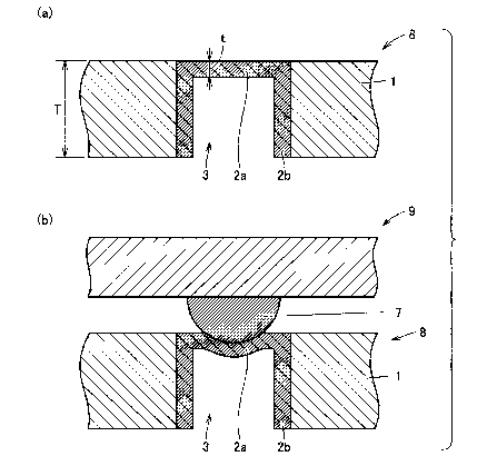
Figure 1 includes diagrams showing a structure and mounting condition of
an anisotropic conductive sheet of the present invention. As shown in Fig.
1(a),
the anisotropic conductive sheet of the present invention is an anisotropic
CA 02628772 2008-05-06
8
conductive sheet 8 having conductivity in the thickness direction, wherein the
base film thereof is a film 1 made of synthetic resin having electrical
insulation
property and the base film has a plurality of holes 3 formed in the thickness
direction. The hole 3 is open to one main surface of the base film and closed
to
the other main surface, wherein the closed part 2a and the inner wall 2b of
the
hole 3 are provided with a metal. Figure 1(b) shows a condition in which a
semiconductor wafer 9 is mounted onto the anisotropic conductive sheet 8. As
shown in Fig. 1(b), the main surface on the side where the hole 3 is open can
electrically be connected through the metal adhered to the inner wall 2b and
the closed part 2a of the hole 3 to the electrode 7 of the semiconductor wafer
9
by contacting the electrode 7 with the closed part 2a from the outside.
[0015]
The base film 1 is preferably a porous film, which is a flexible elastic
sheet;
hence the base film can softly connect with an electrode 7 of a semiconductor
wafer 9 in such a manner as to wrap the surface of the electrode 7 as the
closed
part of the hole 3 bends as shown in Fig. 1(b) when the film touches the
electrode. Thus, it is possible to achieve highly reliable connection by
flexibly
absorbing variations in the height of connecting electrodes. Also, highly
reliable
connection can be obtained, because connection can be made by absorbing a
variation in the position of the electrode 7 even if the semiconductor wafer 9
suffers from thermal expansion or contraction due to temperature variation,
resulting in displacement between the center of the hole 3 and the center of
the
electrode 7. Thus, the anisotropic conductive sheet of the present invention,
CA 02628772 2008-05-06
9
which has heat and cold resistance properties, can be used under a severe
environment such as a burn-in test performed under a high temperature
atmosphere of 150 C or higher, or a cold resistance test conducted at a low
temperature of -30 C or lower.
[0016]
Figure 2 includes diagrams showing a structure and mounting condition of
an anisotropic conductive sheet having a through hole that is outside of the
present invention. As shown in Fig. 2(a), when the diameter of an electrode 27
of a semiconductor wafer 29 is smaller than the diameter of a through hole 23,
there may be a case where electrical connection cannot be obtained even if the
electrode 27 is pressed onto an anisotropic conductive sheet 28. Also, when
the
diameter of the electrode 27 of the semiconductor wafer 29 is larger than the
diameter of the through hole 23 as shown in Fig. 2(b), the end 23a of the
through hole 23 spreads as a result of pressing by the electrode 27, and if
the
elasticity in the surface direction of a base film 21 is not sufficient, the
base
film 21 may fail to fully restore the spread, resulting in degradation of the
connection reliability, and hence inability of repeated use.
[0017]
The hole which is formed in the anisotropic conductive sheet of the present
invention is open to one main surface and closed to the other main surface. As
shown in Fig. 1(b), therefore,.when the electrode 7 is pressed onto the closed
part 2a, the closed part 2a connects flexibly to the electrode 7 in a wrapping
manner, and when the electrode is removed, the closed part 2a recovers its
CA 02628772 2008-05-06
original form. Therefore, regardless of the shape and size of the electrode 7,
a
highly reliable connection can be maintained even if such pressing is
repeated.
Particularly, it is useful in that sure connection is obtained even in the
case of
an electrode which has an inclined side face, such as a solder bump or a
solder
ball. Therefore, the connection method of the present invention, in which a
connection is made by contacting an electrode of a semiconductor chip or a
circuit board with the closed part of a hole of an anisotropic conductive
sheet
from the outside, is advantageous in that flexible and sure connection can be
achieved. Also, the inspection method of the present invention which is
performed in a similar manner is most suitable for the electrical inspection
of a
semiconductor chip or circuit board.
[0018]
The hole of an anisotropic conductive sheet of the present invention is open
to one main surface and closed to the other main surface. Such a structure is
advantageous in that electrical connection can be obtained by deformation with
lower pressure as compared with a hollow structure in which the main surfaces
are both closed. Therefore, according to the present invention, an inspection
can be accomplished without damage or with smaller damage to each electrode
of an inspection article. Also, in an actual inspection, it is possible to
achieve
electrical connection by compressing electrodes on the order of thousands or
tens of thousands of pieces altogether, and accordingly the total load can be
reduced, resulting in reduced damage of inspection articles as a whole, and
hence reduced occurrence of crack, or the like. Also, it is possible to
simplify
CA 02628772 2008-05-06
11
inspection equipment by making the structure suitable for lower load.
[0019]
The base film is a film consisting of synthetic resin and having electrical
insulation property. Thus, by using a material having electrical insulation
property, it is possible to afford the base film with insulation property in
the
surface direction to eliminate the mutual influence of adjacent electrodes.
The
base film is provided with a plurality of holes formed in the thickness
direction,
and a metal is adheres to the closed part and inner wall of the holes.
Therefore,
as shown in Fig. 1(b), by pressing the electrode 7 onto the closed part 2a of
the
hole 3 from the outside, the electrode 7 and the main surface where the hole 3
is
closed are electrically connected together through the metal of the closed
part
2a and the inner wall 2b. Therefore, the conductive sheet of the present
invention has conductivity only in the thickness direction.
[0020]
The synthetic resin for forming a base film is preferably polyester,
polyamide, polyolefin, polyurethane, or the like in view of electrical
insulation
and flexibility, and they can be used in a form of a film, woven fabric,
nonwoven
fabric, or the like. Also, a fluoro-substituted polymer is more preferable
from
the view point of superior heat resistance, chemical resistance,
processability,
mechanical characteristics, dielectric property (low dielectric constant),
etc.
Examples of fluoro-substituted polymers include polytetrafluoroethylene
(hereinafter, also called "PTFE"), tetrafluoroethylene / hexafluoropropylene
copolymer, tetrafluoroethylene / perfluoroalkylvinylether copolymer,
CA 02628772 2008-05-06
12
polyvinylidene fluoride, polyvinylidene fluoride copolymer, ethylene /
tetrafluoroethylene copolymer, etc.; from the view point of heat resistance,
cold
resistance, processability, and mechanical strength, expanded
polytetrafluoroethylene is particularly preferable, which is capable of
maintaining a stable connection without losing elasticity even at a high
temperature of 200 C or more as well as a low temperature of -30 C or less.
Also, it is possible to use engineering plastics such as polyimide,
polyamide-imide, modified polyphenylene ether, polyphenylene sulfide,
polyether ether ketone, polysulfone, polyethersulfone, liquid crystalline
polymer, etc.
[0021]
Since a base film has resiliency and flexibility, by using a porous material
for the base film, it is made possible to ease contact failure due to the
positional
discrepancy of an electrode when a semiconductor wafer is mounted, and hence
to achieve a sure and soft connection. From such a viewpoint, preferably the
mean pore size of the pores contained inside the porous material is 10 um or
less, and the bubble point is preferably 2 kPa or more. Also, from the
viewpoint
of achieving a fine pitch of conductive part, the mean pore size is more
preferably 1 gm or less, and the bubble point is more preferably 10 kPa or
more.
Thus, by making the mean pore size equal to or less than 10 pm, or making the
bubble point equal to or more than 2 kPa, the film strength can be enhanced to
facilitate the ease of its use.
CA 02628772 2008-05-06
13
[0022]
The porosity of the porous material is preferably 20% to 80 %. By making
the porosity equal to or more than 20 %, the resiliency and flexibility of the
porous material can be maintained. On the other hand, by making the porosity
equal to or less than 80 %, sufficient film strength can be secured. The term
"porosity" means a ratio (%) of the volume of pore portions to the whole
volume
of the porous material.
[0023]
As shown in Fig. 1(a), when the hole 3 is formed using a drill, laser beam,
or X ray of synchrotron radiation, the thickness T of the base film 1 can be
made a maximum of 3 mm; preferably 0.1 mm to 2 mm, considering the
processability, though the thicker the better from the viewpoint of securing
sheet flexibility; and T may be 1 mm, for example. Accordingly, it is possible
to
decrease the size and thickness of the anisotropic conductive sheet.
[0024]
A metal can be adhered to the closed part and the inner wall of a hole by
plating with a catalyst adhered to the closed part and the inner wall surface
of
the hole. For such plating, an electroless plating method can suitably be
adopted. First, prior to the electroless plating, a catalyst is adhered to the
inner
wall surface and the closed part of the hole, and thereafter the remaining
catalyst (palladium-tin) is activated. More specifically, the palladium
catalyst is
activated by dissolving tin by means of immersion in such an organic acid salt
for activation of a plating catalyst as is available on the market.
CA 02628772 2008-05-06
14
[0025]
Next, the base film to which the activated catalyst is adhered is immersed
in an electroless plating solution, thereby depositing a conductive metal only
on
the closed part and the inner wall surface of the hole so as to form a
conductive
part (also called "electrically conductive path" or "electrode"). Examples of
such
conductive metals include copper, nickel, silver, gold, nickel alloy, and the
like;
copper is preferable in the case where particularly high conductivity is
necessary.
[0026]
When an expanded porous PTFE sheet is used as the base film, plating
particles (crystal grains) are first deposited, in such a manner as if they
are
entangled, onto the fibrils exposed to the surface of the porous PTFE sheet,
and
the adhering condition of the conductive metal can be controlled by adjusting
the plating time. If the electroless plating time is too short, the quantity
of the
deposited metal will be too small to secure sufficient conduction. In
contrast, if
the electroless plating time is too long, the thickness of the layer in which
the
metal is deposited becomes too thick, resulting in a metallic solid mass, and
accordingly the elasticity restoration power of the porous film will decrease.
By
making the plating quantity moderate so as to adhere the conductive metal
while maintaining a state of porous structure, it is made possible to secure
sufficient resiliency and flexibility, as well as to secure the conductivity
in the
film thickness direction. The thickness of a fibril of the porous film, which
consists of expanded porous PTFE or the like, is preferably 50 pm or less, and
CA 02628772 2008-05-06
the particle diameter of the conductive metal is preferably about 0.001 pm to
5
pm. Also, the quantity of the adhered conductive metal is preferably about
0.01
g/cm3 to 4.0 g/cm3 to maintain porous structure and resiliency.
[0027]
As shown in Fig. 1(b), once the electrode 7 is pressed onto the closed part
2a, the conductive metal of the closed part 2a is pressed to the electrode 7
by
the resiliency of the closed part 2a. Thus, the electrode 7 and the conductive
metal are connected together, and thereby the electrode 7 and the main surface
where the hole 3 is open can electrically be connected together securely
through
the metal of the inner wall 2b. Once the electrode 7 is removed, the closed
part
2a, which consists of a porous film or the like, recovers itself by its
resiliency.
Therefore, the electrode can- repeatedly attached or removed in a case of
inspection, or the like.
[0028]
As shown in Fig. 1(a), the thickness t of the closed part 2a of the hole 3 is
preferably 10 pm to 100 pm, and more preferably 30 pm to 80 pm. By making
the thickness t equal to or more than 10 pm, a sufficient strength against
pressing by the electrode 7 is obtained, and hence the restoration power can
be
secured. On the other hand, when the thickness t is made equal to or less than
100 pm, the metal uniformly adheres to the closed part 2a, securing sufficient
conductivity while maintaining the flexibility of the closed part.
[0029]
From the viewpoint of enhancing electric contactability and prevention of
CA 02628772 2008-05-06
16
oxidation, the metal adhered in this manner is preferably covered with an
antioxidant, precious metal, or alloy of precious metal. The precious metal is
preferably palladium, rhodium, or gold in view of low electric resistance. The
thickness of a coating layer of precious metal or the like is preferably 0.005
pm
to 0.5 pm, and more preferably 0.01 gm to 0.1 pm. If the thickness of the
coating layer is too thin, the improvement in electric contactability is less,
and
if too thick, the coating layer tends to easily peel off. Also, for the
purpose of
coating with gold, it is effective to conduct immersion gold after covering
with a
nickel layer of about 8 nm.
[0030] (Production method of anisotropic conductive sheet)
Embodiment 1
A production method of the present invention for making an anisotropic
conductive sheet is characterized in that a hole is formed in the thickness
direction by irradiating an X-ray of synchrotron radiation or a laser beam.
Figure 3 includes diagrams showing the steps of manufacturing an anisotropic
conductive sheet of the present invention. First, as shown in Fig. 3(a), a
polytetrafluoroethylene sheet having a thickness of 600 pm, for example, is
- -- - -- - -prepared as a base film 31b, and sacrifice layers 31a and 31c are
formed on the
two main surfaces of the base film 31b. The sacrifice layers 31a and 31c are
preferably made of the same material, that is, polytetrafluoroethylene, in
view
of enhancement of exfoliation and adhesion with the base film 31b. The
sacrifice layers 31a and 31c, respectively having a thickness of about 100 pm,
can be formed by hot-melt adhesion or the like.
CA 02628772 2008-05-06
17
[0031]
Next, as shown in Fig. 3 (b), holes are formed in the thickness direction in
the following manner: laser beams or X-rays 38b of synchrotron radiation is
irradiated through a mask absorber having a given pattern while the radiation
energy and irradiation time is adjusted, and thereby the sacrifice layer 31c
and
the base film 31b are partially decomposed and removed.
[0032]
Preferably, the X-ray to be irradiated is an X-ray of synchrotron radiation.
In the case of ablation by the X-ray of synchrotron radiation, a plurality of
predetermined holes can be formed at the same time only in one process of
exposure, and the developing process after exposure is unnecessary. Moreover,
since the ablation speed is so fast as 100 pm/minute, the photon cost can
substantially be reduced, allowing easy processing at a large aspect ratio: a
width of tens of pm and a height of thousands of pm. Also, the predetermined
hole can be formed with a laser beam as well: the size and cost of equipment
are
small; the processing is easy; and as in the case of X-ray by synchrotron
radiation, it is easy to achieve a fine pitch of electrode. Particularly, if a
laser
beam having a short pulse of 10 ps or less is used, the hole can be formed
without destroying the microstructure of the base film. Also, it is possible
to
form such a hole using a drill which will be described in Embodiment 2.
[0033]
Next, as shown in Fig. 3(c), a metal is adhered by electroless plating. The
plating method is superior in productivity and capable of affording electrical
CA 02628772 2008-05-06
18
conductivity at once. There are various ways in the electroless plating
method;
in the case of electroless copper plating, for example, it may be done as
follows: a pre-dip is done using CR-3023 made by Nikko Metalplating; next, a
catalyst
to be used may be CP-3316 made by Nikko Metalplating, and plating promoters
may be NR-2 A and NR-2B, which are made by Nikko Metalplating, and
NKM554 made by Nikko Metalplating may be used for plating.
[0034]
After that, sacrifice layers 31a and 31c1 are peeled off, then an anisotropic
conductive sheet of the present invention, such as a sheet 30 shown in Fig.
3(d),
is obtained. This anisotropic conductive sheet 30 has a base film 31, which is
a
porous film made of polytetrafluoroethylene and having an electrical
insulation
property, and the base film 31 has a plurality of holes 33 formed in the
thickness direction. The holes 33 are open to one main surface of the base
film
31 and closed to the other main surface, and a metal is adhered to the closed
part 32a and inner wall 32b of the holes 33. Thus, by contacting an electrode
with the closed part 32a of the hole 33 from the outside, the electrode and
the
main surface where the hole 33 is open are electrically connected through the
adhe _red metal, and thereby electrical conductivity in the thickness
direction is
achieved.
[0035]
Embodiment 2
Another embodiment of the production method of the present invention for
making an anisotropic conductive , sheet is characterized in that a hole is
CA 02628772 2008-05-06
19
formed with a drill in the thickness direction. Figure 4 includes diagrams
showing production processes of the present invention for making an
anisotropic conductive sheet. First, as shown in Fig. 4(a), sacrifice layers
41a
and 41c made of polytetrafluoroethylene and each having a thickness of 100 pm
are formed on two main surfaces of a base film consisting of a
polytetrafluoroethylene sheet having a thickness of 1 mm.
[0036]
Next, as shown in Fig. 4(b), a hole is formed with a drill 48b from the side
of the sacrifice layer 41c at a predetermined depth in the sacrifice layer 41c
and
the base film 41b. A given hole can be formed with a laser beam or an X-ray of
synchrotron radiation; however, by forming the hole with a micro drill, the
production cost can be reduced since the equipment for generating laser or
X-ray is expensive. For example, a hole having a diameter of 100 pm or more
can simply be formed using a driIl (e.g., hard metal microdrill, SCMMR, made
by Daiwa Seiko, Co., Ltd.) having a blade diameter of 100 lim or more and a
blade length of 1.5 mm or more.
[0037]
Inorder to improve processability, a preferable mode is such that a porous
polytetrafluoroethylene sheet is filled with fused paraffin and solidified by
cooling prior to the drilling process. In such embodiment, the hole portion of
porous PTFE can be suppressed from being deformed or collapsed by the
mechanical load due to the drill processing. The filled paraffin can easily be
removed with xylene or the like after the drilling process.
CA 02628772 2008-05-06
[0038]
Another preferable mode is such that the mechanically formed hole of a
PTFE sheet, which tends to suffer from roughness of its sidewall surface or
destruction of the hole after the drill processing, is subjected to.slight
etching of
the sidewall so that the sidewall is restored. The etching can be done with an
etching solution which contains an alkali metal. Also, the alkali metal is
preferably sodium or lithium.
[0039]
Next, catalyst particles (not illustrated) which facilitate a reduction
reaction are adhered to the whole surface including the closed part 42a and
inner wall 42b of the hole as shown in Fig. 4(c). For example, for the purpose
of
electroless copper plating, Pd-Sn colloid catalyst imparting solution is
impregnated as the catalyst. After that, as shown in Fig. 4(d), the sacrifice
layers 41a and 41c1 are peeled off. The removal of the sacrifice layers
results in
a state where the catalyst particles for facilitating the electroless plating
are
formed only on the closed part 42a and inner wall 42b of the hole.
Subsequently,
the electroless plating is performed, whereby the metal adheres only to the
closed part 42a and inner wal142b of the hole. Thus, an anisotropic conductive
sheet 40 as shown in Fig. 4(e) is obtained.
[0040]
The anisotropic conductive sheet 40 thus obtained comprises a base film
consisting of a porous film 41 made of synthetic resin and having an
electrical
insulation property, and the base film has a plurality of holes 43 formed in
the
= CA 02628772 2008-05-06
21
thickness direction. The hole 43 is open to one main surface of the base film
and
closed to the other main surface, and the metal is adhered to the closed part
42a and inner wall 42b of the hole 43. Consequently, by contacting an
electrode
with the closed part 42a of the hole from the outside, the electrode and the
main surface where the hole 43 is open is electrically connected through the
metal. Thus, the anisotropic conductive sheet has electrical conductivity in
the
thickness direction.
[0041]
This embodiment also is superior in respect of productivity since electrical
conductivity can be afforded at once by plating. Also, the anisotropic
conductive
sheet of the present invention can be manufactured by performing electroless
plating without providing catalyst particles as in Embodiment 1; however this
embodiment is favorable in that it is possible to efficiently plate solely on
the
region that is intended to be plated, that is, the closed part 42a and inner
wall
42b of the hole 43.
[0042]
The hole of the anisotropic conductive sheet of the present invention has
__anopening in the direction of one main surface and the direction of the
other
main surface is closed. Such mode is easier to form a hole and to control the
thickness t of the closed part as compared with a mode in which a hole has a
hollow structure that is closed in both of the main surfaces. Also, it is
possible
to easily adhere a metal to the closed part and inner wall of the hole by
causing
a plating solution to permeate from the opening.
CA 02628772 2008-05-06
22
[0043]
It should be understood that the embodiments and examples disclosed
herein are exemplary and not restrictive in all respects. The scope of the
present invention is intended to be shown, not by the above description, but
by
the scope of a claim, including all modifications and equivalents thereof.
Industrial applicability
[0044]
The anisotropic conductive sheet of the present invention is easy to
decrease its size and thickness and to make a pitch of electrodes finer, and
hence it is possible to meet the needs of miniaturization required of
electronic
equipment and information equipment.