Note: Descriptions are shown in the official language in which they were submitted.
CA 02630901 2008-05-23
PCT/EP2006/069028 - 1 -
2005P11964W0US
Description
Circuit arrangement and method for operating at least one LED
Technical field
The present invention relates to a circuit arrangement and a
method for operating at least one LED (Light Emitting Diode).
Prior art
LEDs are increasingly making inroads into general lighting on
account of their advantages. Cost-effective operating circuits
are desired in this context. So-called SELV (Safety Extra Low
Voltage) power supplies have been used hitherto, which provide
a safety extra low voltage that is potential-isolated from the
mains for the supply of the LEDs. In this case, the prior art
expends a huge outlay in terms of circuitry in order to ensure
the functions of power factor correction, potential isolation,
control of the output voltage or of the output current, and
protective measures against overload and short circuit.
Summary of the invention
The object of the present invention is to provide a circuit
arrangement and a method of operating at least one LED which
enable a plurality of the abovementioned functions to be
implemented with the least possible outlay in terms of
circuitry.
CA 02630901 2008-05-23
PCT/EP2006/069028 - 2 -
2005P11964WOUS
This object is achieved by means of a circuit arrangement
having the features of patent claim 1 and also by means of an
operating method having the features of patent claim 10.
The present invention is based on the insight that the above
object can be achieved by means of a circuit arrangement
comprising an inverter, which operates the at least one LED via
a matching network with a resonant circuit, wherein the
inverter is corrected with regard to the power factor and the
mains current harmonics by means of a pump circuit.
If the main energy store were charged directly from the first
rectifier, then charging current spikes would arise which would
lead to a contravention of the relevant specifications, e.g.
IEC 1000-3-2.
The topology of a charge pump comprises the coupling of the
rectifier to the main energy store via an electronic pump
switch. As a result, a pump node arises between the rectifier
and the electronic pump switch. The pump node is coupled to the
inverter output via a pump network. The pump network can
contain components which can simultaneously be assigned to the
matching network. The principle of the charge pump consists in
the fact that during one half-cycle of the inverter frequency,
energy is drawn from the mains voltage via the pump node and is
buffer-stored in the pump network. In the subsequent half-cycle
of the inverter frequency, the buffer-stored energy is fed to
the main energy store via the electronic pump switch.
CA 02630901 2008-05-23
PCT/EP2006/069028 - 3 -
2005P11964WOUS
Energy is accordingly drawn from the mains voltage with the
turning of the inverter frequency. The spectral components of
the mains current which are at the inverter frequency or lie
above the latter can be suppressed by filter circuits. The
charge pump can thus be designed such that the harmonics of the
mains current are so small that said specifications are
complied with.
One preferred embodiment is distinguished by the fact that it
comprises a second rectifier, in particular a full-bridge
rectifier, which is coupled between the matching network and
the connection terminals for the at least one LED. This measure
ensures that the entire energy provided by the matching network
is made available to the at least one LED in a form, i.e. with
a current direction, in which it can be converted into light by
the LED. This measure therefore leads to a high efficiency of a
circuit arrangement according to the invention.
Preferably, the circuit arrangement furthermore has at least
one coupling capacitor, and the matching network comprises an
LC series resonant circuit, wherein the rectifier input of the
second rectifier is coupled to the high point of the LC series
resonant circuit, on the one hand, and to the at least one
coupling capacitor, on the other hand. At least one coupling
capacitor in series with the inductance of the LC series
resonant circuit prevents a DC current through said inductance
and thus the latter's magnetic saturation and effectiveness as
a current-limiting element. The voltage swing at the input of
the second rectifier in relation to the voltage present at the
CA 02630901 2008-05-23
PCT/EP2006/069028 - 4 -
2005P11964WOUS
inverter determines the quality of the correction of the mains
current harmonics.
Preferably, a transformer is coupled between the matching
network and the connection terminals for the at least one LED.
As a result, potential isolation between the circuit
arrangement and the at least one LED can be realized in a
simple manner.
In this case, it is particularly preferred if the primary side
of the transformer is coupled to the matching network and the
secondary side of the transformer is coupled to the connection
terminals for the at least one LED, wherein a second rectifier,
in particular a full-bridge rectifier, is coupled between the
secondary side of the transformer and the connection terminals
for the at least one LED.
When a second rectifier is used, it is preferred if an
inductance is arranged in series with the rectifier output and
with the connection terminals for the at least one LED. This
measure reduces the ripple of the current fed to the at least
one LED.
One preferred development of a circuit arrangement according to
the invention furthermore comprises a controller, at the
controller output of which an actuating signal can be provided,
wherein the controller output is coupled to the inverter in
such a way that the actuating signal influences the inverter
frequency. In this case, the controller input is preferably
coupled to a device for measuring a quantity that is
proportional to the current through the at least one LED. It is
thereby possible, in a particularly advantageous manner, for
the LED current to be controlled to a predeterminable value,
taking
CA 02630901 2008-05-23
PCT/EP2006/069028 - 5 -
2005P11964WOUS
account of the load, that is to say the number of LEDs used,
the mains voltage and the component tolerances of the entire
circuit.
Further advantageous embodiments of the invention emerge from
the subclaims.
The preferred embodiments mentioned with regard to a circuit
arrangement according to the invention, and their advantages,
are correspondingly applicable to the operating method
according to the invention.
Brief description of the drawing(s)
An exemplary embodiment of a circuit arrangement according to
the invention will now be described in more detail below with
reference to the accompanying drawings, in which:
Figure 1 shows a block diagram for a circuit arrangement
according to the invention for operating at least one
LED;
Figure 2 shows an exemplary embodiment of a circuit
arrangement according to the invention for operating
at least one LED; and
Figure 3 shows the temporal profile of the current Imains drawn
from the mains and of the current ILED through the one
LED in the circuit arrangement in accordance with
Figure 2.
Preferred embodiment of the invention
Figure 1 illustrates a block diagram for a circuit arrangement
according to the invention for operating at least
CA 02630901 2008-05-23
PCT/EP2006/069028 - 6 -
2005P11964WOUS
one LED. A mains voltage from a mains voltage source can be fed
to the circuit arrangement at connection terminals J. The mains
voltage is firstly fed into a block FR. On the one hand, said
block contains known means for filtering interference and, on
the other hand, said block contains a rectifier that rectifies
the mains voltage, which is usually an AC voltage but can also
be a DC voltage. A bridge-connected full-wave rectifier is
usually used for this purpose. The property of the rectifier
that it does not permit any current that would mean a f low of
energy from the circuit arrangement to the mains voltage source
is important for the function of a charge pump realized in the
circuit arrangement.
The rectified mains voltage is fed to an electronic pump switch
UNI, wherein a pump node Nl arises at the junction point
between rectifier FR and electronic pump switch UNI. In the
simplest case, the electronic pump switch UNI comprises a pump
diode that only allows a current flow that flows from the pump
node Ni to the pump diode. However, it is also possible to use
any desired electronic switch, such as a MOSFET, for example,
for the electronic pump switch UNI which fulfils the function
of the pump diode. The current which the electronic pump switch
UNI allows to pass feeds a main energy store STO. The main
energy store STO is usually embodied as an electrolytic
capacitor. However, other types of capacitors are also
possible. In principle, the dual form of energy storage with
respect to the capacitor is also possible. In the dual case,
the main energy STO is embodied
CA 02630901 2008-05-23
PCT/EP2006/069028 - 7 -
2005P11964WOUS
as a coil. Owing to the lower costs and the better efficiency,
a capacitor is preferred as the main energy store STO.
There are also embodiments of charge pumps having a plurality
of so-called pump branches. In this case, a plurality or
electronic pump switches UNI are connected in parallel. A
plurality of pump nodes Nl arise as a result. For the mutual
decoupling of the pump nodes, a diode is in each case connected
between rectifier and pump node.
The main energy store STO makes its energy available to an
inverter INV. The inverter INV generates an alternating
quantity, usually an alternating voltage, which is fed to a
block designated by MN and PN. MN designates the function of
the block as a matching network. With regard to this function,
the block MN/PN can be connected to at least one LED via a
further rectifier GR and an inductance L. In this case, the
rectifier GR ensures that current is made available to the at
least one LED only in the direction in which it can be
converted into light by the LED. The inductance L, which can
also be realized by a transformer, serves for reducing the
ripple of the current ILED flowing through the at least one LED.
PN designates the function of the block as a pump network. With
regard to this function, the block MN/PN is connected to the
pump node Nl. The connecting line between the pump node Nl and
the block MN/PN is provided with an arrow at both ends in
Figure 1. This is intended to indicate that energy flows
alternately from the pump node Ni to the block MN/PN and back.
The functions of the matching network and of the pump
CA 02630901 2008-05-23
PCT/EP2006/069028 - 8 -
2005P11964WOUS
network are combined in the block MN/PN because embodiments of
the invention are possible in which individual components can
be assigned both to one function and to the other function.
A controller CONT is provided for controlling a desired
operating quantity, said controller acting on the inverter INV
by means of a manipulated variable. A parameter of the
alternating quantity output by the inverter, for example the
operating frequency and/or the pulse width, is thus altered in
such a way that an alteration of the operating quantity is
counteracted. The operating quantity is fed to an input of the
controller CONT via the connection B1. The operating quantity
is a quantity that determines the operation of the LED, for
example the current ILED through the LED. In Figure 1,
therefore, the connection Bl originates from the block for the
LED. Instead of the current ILED through the LED, for example
the power converted in the LED can also form the operating
quantity. These quantities do not have to be detected directly
at the LED, but rather can also be taken from the block MN/PN.
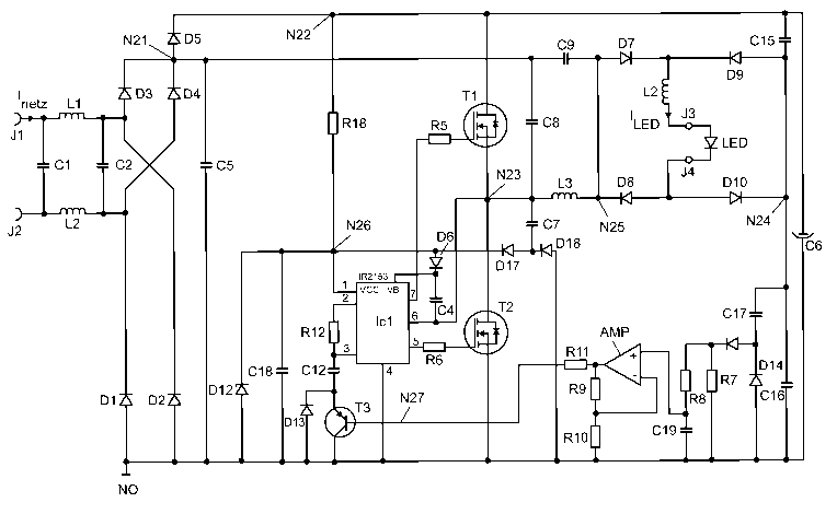
Figure 2 illustrates an exemplary embodiment of a circuit
arrangement according to the invention for operating at least
one LED.
A mains voltage can be connected to the connections J1 and J2.
Via a filter, comprising two capacitors Cl, C2 and two coils
Li, L2, the mains voltage is fed to a full-bridge rectifier,
comprising the diodes Dl, D2, D3, D4. The full-bridge rectifier
provides the rectified mains voltage at its positive output, a
node N21, with respect to a reference
CA 02630901 2008-05-23
PCT/EP2006/069028 - 9 -
2005P11964WOUS
node NO. The node N21 is simultaneously a pump node. In this
case, it should be taken into consideration that the diodes Dl
to D4 used in the rectifier must be able to switch fast enough
to follow the inverter frequency. If this is not the case, a
fast diode can be connected between rectifier output and pump
node.
From the pump node N21, an electronic pump switch, embodied as
a diode D5, leads to the node N22. The main energy store,
embodied as an electrolytic capacitor C6, is connected between
N22 and NO. The capacitor C6 feeds the inverter, embodied as a
half-bridge in the present case. However, other converter
topologies, such as flyback converter or full-bridge, for
example, can also be used.
The half-bridge illustrated in the exemplary embodiment in
Figure 2 comprises the series circuit formed by two half-bridge
transistors Tl and T2 and the series circuit formed by two
coupling capacitors C15 and C16. Both series circuits are
connected in parallel with C6. A connecting node N23 of the
half-bridge transistors and a connecting node N24 of the
coupling capacitors C15, C16 form the inverter, at which a
trapezoidal inverter voltage having an inverter frequency is
present. An inductance L3 is connected between the node N23 and
a node N25. A capacitor C8 acts as a trapezoidal capacitor.
Energy for supplying an integrated circuit IC1, which will be
discussed in greater detail further below, is tapped off via a
capacitor C7. Since a trapezoidal voltage is present at the
node N23 during operation of the inverter, a current flow is
produced through
CA 02630901 2008-05-23
PCT/EP2006/069028 - 10 -
2005P11964WOUS
the capacitor C7 during these times. In this case, the positive
half-cycle is used via the diode D17 for supplying the circuit
IC1 with current, while the negative half-cycle is conducted
away via the diode D18 to the reference potential NO. The node
N25 is connected to the pump node N21 via a first resonance
capacitor C9. A second resonance capacitor C5 is connected
between N21 and NO. C9 and C5 together with the inductor L3
form a resonant circuit. The inductor L3 interacts with C9 and
C5 as a matching network which transforms an output impedance
of the inverter into an impedance necessary for the operation
of the at least one LED. By virtue of the connection of C9 and
CS to the pump node N21, however, the combination of L3, C9 and
C5 acts not only as a resonant circuit and matching network,
but simultaneously as a pump network. If the potential at N21
is lower than the instantaneous mains voltage, then the pump
network L3, C9, C5 draws energy from the mains voltage. If the
potential at N21 exceeds the voltage at the main energy store
C6, then the energy taken up from the mains voltage is emitted
to C6. The effect of the network L3, C9, C5 as a pump network
can be adjusted through the choice of the ratio of the
capacitances of C9 and C5. The larger the capacitance of C5 is
chosen to be, the smaller the effect of the network L3, C5, C9
as a pump network. A further pump effect proceeds from the
capacitor C8 connected between N23 and N21. C8, too, does not
just act as a pump network but also fulfils, as mentioned, the
task of a trapezoidal capacitor. Trapezoidal capacitors are
generally known as a measure for switch load relief in
inverters.
CA 02630901 2008-05-23
PCT/EP2006/069028 - 11 -
2005P11964WOUS
The matching network is followed by a second full-bridge
rectifier, which is formed by the diodes D7, D8, D9 and D10.
Said diodes ensure that the LED is fed a current having only
one direction. A constant-current inductor L2 is arranged
between the rectifier output and the connections J3, J4 for the
at least one LED, said inductor providing for a reduction of
the ripple of the current ILED fed to the at least one LED. In
the case of a desired potential isolation between a circuit
arrangement according to the invention and the at least one
LED, the constant-current inductor L2 can be realized by a
transformer, wherein the second rectifier D7 to D10 is then
arranged on the secondary side of the transformer.
Besides the illustrated variant with one pump branch, exemplary
embodiments with two or more pump branches are readily
conceivable, in which the pumped energy is shared between a
plurality of components. A more cost-effective dimensioning of
the components is thus possible. This also yields a degree of
freedom in the design of the dependence of the pumped energy on
operating parameters of the at least one LED.
The half-bridge transistors Tl, T2 are designed as MOSFETs.
Other electronic switches can also be used for this purpose. In
the exemplary embodiment, an integrated circuit IC1 is provided
for driving the gates of the transistors T1 and T2 via the
resistors R5 and R6. In the present example, IC1 is a circuit
from the company International Rectifier of the type IR2153.
Alternative circuits to this type are also commercially
available, for example an L6571 from the company STM. The
CA 02630901 2008-05-23
PCT/EP2006/069028 - 12 -
2005P11964W0US
circuit IR2153 contains a so-called high-side driver, which can
also be used to drive the half-bridge transistor T1 even though
it does not have a connection at the reference potential NO. A
diode D6 and a capacitor C4 are necessary for this purpose. IC1
is supplied with operating voltage via the connection 1 of IC1.
In Figure 2, for this purpose the connection 1 is connected to
a node N26, which is coupled to the node N22 via a resistor
R18. The voltage at the node N26 is held at a predeterminable
value by means of a zener diode D12 and provided to IC1 via a
capacitor C18. As an alternative, by way of example, the
component IC1 could be supplied by the rectified mains voltage
via a resistor.
In addition to the driver circuits for the half-bridge
transistors T1, T2, IC1 comprises an oscillator, the
oscillation frequency of which can be set via the connections 2
and 3. The oscillation frequency of the oscillator corresponds
to the inverter frequency. A frequency-determining resistor R12
is connected between the connections 2 and 3. The series
circuit formed by a frequency-determining capacitor C12 and the
emitter-collector path of a bipolar transistor T3 is connected
between the connections 3 and NO. A diode D13 is connected in
parallel with the emitter-collector path of T3 in order that
the capacitor C12 can be charged and discharged. The inverter
frequency can be set by a voltage between the base connection
of T3 and NO and thus forms a manipulated variable for a
control loop. The base connection of T3 is connected to a
manipulated variable node N24. T3, IC1 and the circuitry
thereof can therefore be interpreted as a controller.
CA 02630901 2008-05-23
PCT/EP2006/069028 - 13 -
2005P11964WOUS
The functions of IC1 and the circuitry thereof can also be
realized by any desired voltage- or current-controlled
oscillator which realizes the driving of the half-bridge
transistors by means of driver circuits.
The control loop in the exemplary embodiment detects the
current ILED through the LED as controlled variable. For this
purpose, a quantity proportional to the current ILED is fed via
the capacitor C17 and the diodes D14 and D15 to a low-
resistance measuring resistor R7. The voltage drop at R7 is
therefore a measure of the current through the at least one
LED. Via a low-pass filter for averaging, which is formed by a
resistor R8 and a capacitor C19, the voltage drop passes to the
input of a non-inverting measuring amplifier. The measuring
amplifier is realized by an operational amplifier AMP and the
resistors R9, Rl0 and Rll in a known manner. In the exemplary
embodiment, a gain of the measuring amplifier of approximately
is set. For the case where the voltage drop at R7 has values
which can be used directly as a manipulated variable, the
measuring amplifier can be omitted or replaced by an impedance
converter, such as an emitter follower for example.
The output of the measuring amplifier is connected to the node
N27. This closes the control loop for controlling the current
through the LED. By raising the oscillator frequency, a
reduction of the current ILED flowing through the at least one
LED is obtained on account of an inductive load circuit.
CA 02630901 2008-05-23
PCT/EP2006/069028 - 14 -
2005P11964WOUS
Figure 3 shows, in a schematic arrangement, the temporal
profile of the mains current Imains and of the current ILED
through the at least one LED in a circuit arrangement in
accordance with Figure 2. The modulation - still discernible in
Figure 3 - of the current ILED flowing through the at least one
LED - a 100 Hz modulation that is superposed by a high-
frequency signal is involved in the present case - can be
reduced further by an optimization of the control mentioned
above, while the HF ripple can be reduced by enlarging the
constant-current inductor L2.