Note: Descriptions are shown in the official language in which they were submitted.
CA 02631179 2008-05-27
WO 2007/061286 PCT/NL2005/000816
1
Title: OPTICAL DEVICE COMPRISING A CANTILEVER AND METHOD OF
FABRICATION AND USE THEREOF
The present invention relates to an optical device comprising a
cantilever, to a method a fabrication thereof and to a method of
measuring a displacement of a cantilever.
Micromachined cantilevers are the most elementary and
successful example of miniaturized sensors. A cantilever, comprising
a free-standing beam can often detect changes in the chemical,
biological and/or physi.cal properties of the surroundings with
sensitivity comparable, if not superior, to much more complicated
devices. It is thus not surprising that this simple design is still
at the heart of several commercially available instruments,
including, but not limited to, an Atomic Force Microscope (AFM). A
description of the AFM can be found in G. Binnig, C. F. Quate, Ch.
Gerber, Phys. Rev. Lett. 56, 930 (1986), which is included herein by
reference.
These instruments rely on the possibility to measure a
displacement of the suspended part of the beam perpendicular to its
length with up to atomic accuracy, a level of precision that can for
instance be achieved by electronic or optical read-out. Methods of
measuring the displacement of the suspended part include for instance
tunneling probes (G. Binnig, C. F. Quate, Ch. Gerber, Phys. Rev.
Lett. 56, 930 (1986)), integrated field-effect transistors (R. G.
Beck, et al., Appl. Phys. Lett. 73, 1149 (1998)), capacitive methods
(J. Brugger, N. Blanc, Ph. Renaud, N. F. de Rooij, Sens. Actuators,
A43, 339 (1994)), piezoelectric or piezoresistive devices (J.
.25 Tansock, C. C. Williams, Ultramicroscopy 42-44, 1464 (1992)), optical
levers (M. Tortonese, R. C. Barrett, C. F. Quate, Appl. Phys. Lett.
.62, 834 (1992), or G. Meyer, N. M. Amer, Appl. Phys. Lett. 53, 1045
(1988)); or optical fiber interferometers (S. Alexander, et al., J.
Appl. Phys. 65, 164 (1989), D. Rugar, H. J. Mamin, R. Erlandsson, B.
D. Terris, Rev. Sci. Instr., 59, 2337 (1988) or A. D. Drake, D. C.
Leiner, Rev. Sci. Instr. 55, 162 (1984)).
Electronic read-outs may be incompatible with the environment
where measurements must be performed. Examples of such environments
CA 02631179 2008-05-27
WO 2007/061286 PCT/NL2005/000816 _
2
are electrically conductive liquids or extreme temperatures.
Furthermore, fabrication of the measurement devices involves
cumbersome and expensive processes,. an important detail that has
limited their cominercial and scientific impact. Optical techniques
are more widespread than electronic techniques, as their application
faces fewer limitations. However, optical techniques generally
require an inconvenient, time consuming alignment.procedure, which
represents a major technical challenge for applications beyond
standard experiments.
10. The present invention aims to provide an improved device, to
render application thereof more convenient.
Accordingg to a first aspect, this aim is achieved by an optical
device, comprising: - an optical fiber; .
- a cantilever that is arranged on an end of the optical fiber.
The present device is for instance suitable for AFM
measurements in critical environments and for any other application
where a cantilever may be used. The cantilever is correctly aligned
relative to the optical fiber by incorporating the cantilever in an
end of the optical fiber. The displacement sensitivity of such an
arrangement proves to be comparable to commercially available AFMs.
Thus, fiber-top cantilevers can be successfully used not only in
critical environments, but also'in standard experiments.
In-an embodiment, the cantilever is an integral part of the
optical fiber. Because of this monolithic.structure, the device does
.not require any alignment procedure, not even in case of relatively
large temperature fluctuations, and corresponding expansion or
shrinkage, during use.
In an embodiment the cantilever has a length that is
substantially equal to a diameter of the optical fiber. Rendering the
length of the cantilever in the order of the diameter of the optical
-fiber improves the sensitivity of the device. Substantially equal may
be regarded as the diameter +/- 10%.
Measurement means for measuring a displacement of the
cantilever may be connected to an opposite end of the optical fiber.
The measurement means may comprise a laser. The laser may be arranged
for directing light into the optical fiber.
Optionally, the cantilever has two opposite ends, wherein one
end is anchored to the optical fiber and the opposite end is free-
ranging.
CA 02631179 2008-05-27
WO 2007/061286 PCT/NL2005/000816
3
Other embodiments comprise cantilevers having a different
geometry. The cantilever may comprise a beam having a widened plate
in the middle. In an embodiment, the two opposite ends of the
cantilever are both fixed to the optical fiber, and a part of the
cantilever.between the two ends is freely suspended over the optical
fiber. This embodiment is referred to as a bridge configuration.-
Optionally, the measurement means include a high frequency
filter to reduce the noise level and to improve the sensitivity. The
sens'itivity of the device may be below 4 A. In an improved
embodiment, the sensitivity of the device is superior to atomic
level, for instance in the order of 0.4 to 0.2 A.
Preferably, the cantilever comprises.glass and/or silica. I.e.,
the cantilever may be fabricated from the same material as a light-
conducting core of the optical fiber. This cantilever comprises fewer
components. The accuracy can be comparable to commercially available
AFMs.
In a further embodiment the cantileverand/or the a part of the
end of the optical fiber may be coated with a reflection layer. The
reflection layer optionally comprises a.metal such as silver, gold or
platinum. Adding the reflection layer increases measurement
performance. A thickness of the metallic reflection layer may be in
the order of 100 nm. The reflection layer improves the reflection of
light, and thus improves the sensitivity when the device is used as
an interferometer.
25. According to a second aspect, the present invention provides a
method of fabricating an optical.device, comprising the steps of:
- providing an optical fiber;
- arranging a cantilever on an end of the optical fiber.
In an embodiment, arranging a cantilever on an end of the
optical fiber comprises the further steps of:
- coating the optical fiber with a metallic layer to prevent
electrostatic charge accumulation; and
- machining the end of the optical fiber to obtain the cantilever as
an integral part of the optical fiber.
In an embodiment, the step of machining the end of the optical
fiber is followed by the step of depositing a reflection layer on a
part of the end of the optical fiber and/or on the cantilever.
According to a third aspect, a method of measuring a
displacement using the optical device as described above is provided,
the method comprising the steps of:
CA 02631179 2008-05-27
WO 2007/061286 PCT/NL2005/000816
4
- arranging measurement means, comprising a light source, on an
opposite end of the optical fiber;
- using the light source to send.a beam of light into the optical
fiber;
- measuring the interference.of light that is reflected on the end of
the optical fiber and light that is reflected on the cantilever;
- determining the position of the cantilever relative to the optical
fiber dependent on the measured interference.
Further advantages and details will become apparent in the
light of the following drawings, wherein:
Fig. 1 shows a perspective view of a first embodiment of the
optical device according to the present invention;
Figs. 2A, 3A, 4-7 show diagrams of further embodiments of the
optical device according to the present inventio.n;.
Figs. 2B, 2C show perspective views of exemplary embodiments
comprising a cantilever having a fixed end and a free-hanging end;
Figs. 3B, 3C show perspective views of exemplary embodiments
comprising a cantilever having a bridge configuration wherein two
ends of the cantilever are fixed to the optical fiber;
Figs. 8-13 show diagrams of subsequent steps of a method for
producing an optical device according to the present invention;
Figs. 9-20 show diagrams of subsequent steps of an alternative
method for producing an optical device according to the present
invention;
Fig. 21 shows a diagram of the use of an optical device
according to the present invention for'measuring a displacement of
the cantilever;
Fig. 22 shows an example-of a read-out during the measurement
of Fig. 21; and
Fig. 23 shows a side view of an embodiment of the optical
device according to the present inventionduring use.
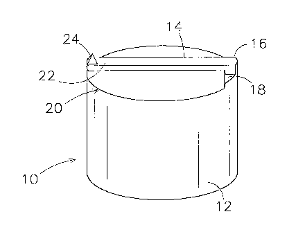
Fig. 1 shows a first embodiment of an optical device 10
according to the present invention. The device comprises an optical
fiber 12. The optical fiber comprises a translucent, elongated
tubular body comprising silica. The tubular body has two opposite
ends that are suitable for inputting and/or outputting light.
Furthermore, the tubular body is flexible and solid, and is able to
guide light signals. Commercially available optical fibers comprise
such a translucent core of silica, surrounded by a translucent
cladding made out of, for instance, doped silica, and an insulating
CA 02631179 2008-05-27
WO 2007/061286 PCT/NL2005/000816
jacket (not shown in Fig. 1). The jacket commonly comprises a
synthetic material.
A cantilever 14 is arranged on the fiber 12. The cantilever
comprises an elongated body having two opposite ends. One of the two
5 opposite ends or both ends are connected to the.optical fiber. A part
of the body of the cantilever between the two ends is freely
.suspended over the optical fiber. This.part has a flexibility that
allows movement of the part in the length direction of the tubular
body of the fiber. Exemplary embodiments of the cantilever are
described below.
.. In the embodiment of Fig. 1, the cantilever is an integral part
of the optical fiber. A first end 16 of. the cantilever is connected
to an elevation 18 of an end 20 of the optical fiber. The elevation
comprises a ridge that extends from the o.ptical-fiber..Oneside of
'the ridge coincides with a wall of the tubular body of the fiber. An
opposite, free end 22 of the cantilever is suspended over the end 20
of the fiber. The ridge creates a space between-the.end 20 of the
fiber and the cantilever, to allow movement of the cantilever in the
length direction of the tubular body of the fiber. Optionally, the
end 22 is provided with an extending tip 24, for instance for
application in an AFM. The cantilever may be connected on the optical
fiber by other means, i.e. form a separate.part.
Examples of an alternative geometry are shown in, but not
limited to, Figs. 2A to 7. Elements that correspond with the
embodiment of Fig. 1 have the same reference numerals as shown in
Fig. 1.
Fig. 2A shows a cantilever 30 comprising a beam having an end
32 that is fixed to end 20'of the optical fiber. At an opposite end
the beam is connected to a round plate 34. The round plate is
substantially suspended over the center of optical fiber 12. The
increased surface of the plate relative to the beam near the center
of the optical fiber improves the reflective properties of the
cantilever.
Fig. 2B shows an embodiment comprising, like the embodiment of
Figs. 1 and 2A, a cantilever having a fixed end 32 that is fixed to
the optical fiber 12. The opposite end of the cantilever is free-
hanging above the end 20 of the optical fiber.
Fig. 2C shows an embodiment wherein a tip 31 is arranged at the
free-hanging end of the cantilever 30. The way of fabricating the tip
31 is described below. The tip 31 is preferably pointed, and may
CA 02631179 2008-05-27
WO 2007/061286 PCT/NL2005/000816
6
comprise a single atom at the end that is facing away from the
cantilever. This is for instance preferred for use of the device in
an AFM. Forces between the tip and a sample provide an indication.of
a surface geometry of the sample".
..Fig. 3A shows an embodiment wherein an elongated cantilever 40
comprises two opposite end's 42,.44 that are fixed to the end 20 of
the optical fiber 12. Two arms.46, 48 connect the fixed ends to a
rectangular plate 50. The plate is suspended over the center-o.f the
end 20 of,the optical fiber. The embodiment of the cantilever shown
in Fig. 3A, comprising two opposite fixed ends and an intermediate
freely.suspended part, is referred to as a bridge-configuration.
Fig. 3B shows a simpler-embodimen.tof the bridge configuration.
A cantilever 38 if fixed to theoptical fiber 12 at two opposite ends
42, 44. The cantilever 38 further includes a beam that connects the
two ends 42, 44. To provide the beam with a suitable flexibility, the
choice of material or the dimensions of the beam, i.e. the thickness
and/or the width, may be varied.
Fig. 3C shows another example of the bridge configuration. The
cantilever 38 is at two ends 42, 44 fixed on the end 20 of the
optical fiber 12. The cantilever comprises two beams 46, 48
connecting the ends 42, 44 with a central table or plate 50. To
increase the flexibility of the cantilever, beams 46, 48 are provided
with at least one indentation, for instance four indentations 52, 54,
56, 58.
Fig. 4 shows an embodiment, wherein.a cantilever 60 comprises a
spiral-shaped arm 62. The arm 62 is on one end 64, which is located
adjacent to the wall of the tubular body of the optical fiber, fixed
to the end 20 of the optical fiber. On the.opposite end, the arm
comprises a round plate 66. The spiral arm increases the length and
the flexibility of the cantilever, relative to the embodiment of Fig.
2A. The increased length and flexibility decreases the force that is
needed to dislocate the free end of the cantilever, and increases the
sensitivity of the optical device.
Fig. 5 shows a cross-shaped cantilever 70 having four crosswise
extending arms 72, 74, 76, 78. The arms are on one end 80, 82, 84, 86.
fixed, adjacent to the edge of the'end 20. In the middle of the end
20, the arms converge into rectangular plate 88. Due to the four-
point fixation the cantilever of Fig. 5 has an improved stability and
rigidity, rendering it suitable for heavy-duty applications wherein
durability and life span are important.
CA 02631179 2008-05-27
WO 2007/061286 PCT/NL2005/000816
7
Fig. 6 shows a cantilever 90 comprising two ends 92, 94 that
are fixed to the optical fiber 12 adjacent the edge of end 20: The
ends 92, 94 are interconnected by a beam 96. In the middle of the
beam 96, a perpendicularly extending second beam 98 is provided. The
second beam 98 has a first end 100 that is arranged on the beam 96.
The opposite freely suspended part of the beam 98 is moveable in the
direction of the length of the optical fiber 12 by torsion of the
beam 96. Application of movement of the cantilever is described
below.
Fig. 7 shows a cantilever 110 having end 112 that is fixed to
the optical fiber 12, adjacent the edge of end 20. From the fixed end
112, two semi-circular arms 114 extend to the opposite side of end 20
of the optical fiber. At the opposite end, the semi-circular arms
extend into V-shaped arm 116 that is provided with a round plate 118.
In a first exemplary method of fabrication, a single-.mode
optical fiber 130 (for instance commercially available SMF-28,
corning: core diameter 9 pm, cladding diameter 125 pm) is cleaved to
a desired length, using a known process (Fig. 8). The fiber is
cleaved substantially perpendicular to its length direction. The
desired length is for instance in the range of 1 to 5 m. The cleaved
optical fiber 132 is stripped of its jacket (Fig. 9), and coated with
a thin conductive layer (comprising metal, for instance 5 nm Cr
and/or 20 nm Pd) to prevent electrostatic charge accumulation in the
next fabrication step. The conductive coating is deposited on the end
20 of the fiber (Fig. 10) as well as on the longitudinal wall of the
fiber, along the length thereof .(Fig. 11). The coated end of the
fiber is micromachinedby means of Focused-Ion-Beam to obtain a
cantilever 134 anchored to the fiber (Fig. 12)..As described above,
the cantilever may be parallel to the end of the fiber (Fig. 13).
Subsequently, a reflection layer is deposited onto the cantilever, to
improve-reflection during interferometry. The reflection layer may
comprise a metal. The thickness of the reflection layer may be in the
order of 100 nm. The reflective layer may be of any reflective
material available. Examples of suitable materials are silver, gold
or platinum.
The above method of fabrication may be complemented by a step
comprising the machining or deposition of a tip on the cantilever
(see Figs. 1 and 2C). The tip can be machined from the same material
as the optical fiber. Machining the tip can for instance be done by
carving the tip out of the cantilever. Arranging the tip may include
CA 02631179 2008-05-27
WO 2007/061286 PCT/NL2005/000816
8
evaporation or deposition of a suitable material, such as a metal, by
other means. Also, growing the tip by a monolayer deposition
technique is an option. The tip may be deposited before or after
deposition of the reflection layer. Conventional AFMs use a
canti.lever having an extending tip at the end of the cantilever.
Thus, the device according to the present invention is suitable for
use in such AFM.
Other.method steps may be used to machine the cantilever. Other
methods include photolithography, e-beam lithography, wet or dry
10'etching. (maybe after implantation, annealing, lift-off, masking,
deposition of metals or other coatings, et cetera), microtome
cutting, laser ablation, diamond cutting, nano-imprinting et cetera.
An example is shown in Figs. 14 to 20. The steps are: -
'Cleaving the optical fiber 138 to a desired length (Fig. 14); -
applying.photo-resist 141, such as PolyMethyl.MethAcrylate (PMMA), at
an end of the cleaved optical fiber.140 (Fig. 15); - expose the
photo-resist 141 with light or electrons to arrange a groove 142
(Fig. 16); - remove the exposed photo-resist (Fig. 17) to create the
groove in end 144 of the translucent core of the cleaved optical
fiber (Figs. 17); - deposit, e.g. by evaporating, a suitable material
146 on the photo-resist and in the groove (Fig. 18); - removing, i.e.
so called lift-off, the photo-resist 141 that encloses the groove
.(Fig. 19); removing material of,the optical fiber, e.g. by etching,
to create, the space between the cantilever and the optical fiber
(Fig. 20).
Thesame device can be obtained by growing.layers on top of the
optical fiber and using conventional micromachining techniques.
Materials to be grown can be distinguished in two main classes:
1) Sacrificial layers, i.e. layers that are used only for
fabrication purposes and that are removed at the end of the
..fabrication process. Examples of sacrificial materials are silica,
quartz, phosphosilicate glass, PolyMethyl MethAcrylate (PMMA),
metals, et cetera; and
2) Mechanical or structural materials, i.e. materials that
perform mechanical duties. Examples of mechanical materials are
crystalline silicon, polycrystalline silicon, silicon nitride,
silicon oxide, metallic layers, et cetera. The materials mentioned
before are preferred due to their compatibility with the material of
.the optical fiber. Examples of micro-fabrication techniques have been
listed above.
CA 02631179 2008-05-27
WO 2007/061286 PCT/NL2005/000816
9
Fig. 21 shows a diagram of an embodiment of an optical read-out
technique.. The technique is applicable to any embodiment of the Figs.
1 tot 7. The displacement of the cantilever 150 relative to the
length of the optical fiber 152 can be determined by measuring the
interference of (laser) light reflected at the fiber-to-air interface
and light that is reflected at the cantilever itself. In Fig. 21,
continuous arrows represent the light input into the optical fiber by
light source 154. Dashed arr.ows-represent the light reflected at the
fiber-to-air, air-to-cantilever,-and/or cantilever-to-reflective
layer interfaces (156, 158.and 160 respectively). In the enlarged
portion of the optical.fiber on the right of Fig. 21, the dark area
in the middle of the fiber represents the beam of laser light 162
travelling through the fiber (not to scale).
When, during use, the optical device of the invention.is
-15 coupl.ed to the read-out iristrumentation sketched -in Fig. 21, the
light of a laser beam coupled to the fiber is partially reflected at
the fiber-to-air 156, air-to-cantilever 158, and cantilever-to-
reflective layer 160 interfaces back into the.fiber. The laser light
is for instance infrared, having.a 1.31 }im wavelength. The three
reflected light signals enter a fiber coupler that transmits for
instance 50% of the optical power.to another fiber aligned with an
infrared sensor. If multiple reflections are-neglected, the output
signal W of the detector, for instance a voltage, is given by
equation (1) :
4711 ~ 4rrnt 4mt
W=W +W +W - WW cos WW co ~ + W W cos
A
where,Wl, W2, and W3 are proportional to the amount of light reflected
at the fiber-to-air, air-to-cantilever, and cantilever-to-metal
interfaces, respectively, d is the separation.i,n meter between the
edge of the.fiber and the inner surface of the cantilever, t is the
thickness of the cantilever in meter, n is the refractive index of
the core of the fiber, and A is the wavelength of the laser in meter.
Equation (1) can be rewritten as equation (2):
W=Wo 1-Vcos( 4~+~p1
CA 02631179 2008-05-27
WO 2007/061286 PCT/NL2005/000816
where cp is a constant, V is the fringe visibility, and Wo is a
midpoint output (Fig. 22) . V and Wo are related to the output signals
corresponding to maximum (W,,,pc) and minimum ( W,;,,) interference
according to the subsequent equations (3) and (4):
5
v W. - Wmin
Wmax + Wmin
W = Wmax + Wmin
0 2
10 The displacement sensitivity close to quadrature is given by
equation (5):
Od~Iz OWl
4TCWoV
where aW is the minimum detectable signal. Herein, quadrature means
the situation wherein the output is equal to Wo, i.e. wlyen the cosine
of equation (2) is zero. The cosine of equation (2) is zero when the
argument of the cosine is an odd multiple of 7t/2..Fquation.'(5) is
derived from equation (2) by making a Taylor series at quadrature:..
=20 Fig. 22 shows the read-out signal obtained in correspondence of
a mechanical deformation of the cantilever, for instance while
touching the cantilever with an external tip and pushing the free end
of the cantilever in the direction of the fiber. The horizontal axis.
represents the time t, and the vertical axis represents the output W
of the measurement device (in voltage V). At time t1, say about 800
ms after starting data acquisition, the cantilever is brought into
contact with the end 20 of the optical fiber 12. The first spike in
the trace corresponds to the approaching movement. The cantilever was
then left in contact with the optical fiber for some time, for
instance about 500 ms, as indicated by the flat part of the signal
between the two spikes. At time t2, the tip was retracted, allowing
the cantilever to return to its initial position. The returning
cantilever produces the second spike of the trace (for instance after
1.5 s). The images below the trace represent the different positions
in which the cantilever h-as been set: (i) freely suspended (before
CA 02631179 2008-05-27
WO 2007/061286 PCT/NL2005/000816
11
contact), (ii) in contact with the edge of the optical fiber, (iii)
freely suspended (after contact).
This experiment demonstrates for instance that the device can
be used as a position sensor. I.e., upon contact with a foreign body,
the output signal of such a sensor changes. Upon retracting of the
sensor, the output signal changes again, until arriving at the
original output indicating that the contact with the foreign body is
broken.
To determine the displacement sensitivity, the micromachined
fiber was anchored to a heatable plate for determining the output
signal as a function of the temperature of the plate. As the
temperature increases, the stress induced by the different thermal
expansion coefficients of the metallic coating and of the material of
the optical fiber makes the cantilever bend. During this deformation
the output signal passes through a minimum and a maximum, as.expected
from previous equations. In a practical embodiment, W,,, is about 3.1
V and W,,,ar is about 4.8 V. The RMS noise of the output signal,
measured with a digital oscilloscope in the whole available bandwidth
(dc-400 MHz) over a 0.2 s time interval, may be about 3.5 mV. The
sensitivity that is achieved corresponds to a displacement of the
cantilever relative to the fiber of about 0.4 nm. It is noted that
the dominant part of the noise is associated to a high frequency
periodic signal generated by the electronic read-out and not by the
fiber itself.
25. The RMS noise value does not change if a standard cleaved
optical fiber, i.e. an optical fiber lacking a cantilever, is plugged
to the read-out system. By adding a high frequency filter at the exit
of the read-out it is possible to reduce the noise level. The
reduction may be down to a few hundreds of }iV. The fringe visibility
may be in the order of 21%.. Improving the alignment of the cantilever
with respect to the core of the fiber provides a higher visibility,
which results in an improved sensitivity. The sensitivity may be
superior to atomic level, for instance in the order of 0.4 to 0.2 A.
Experiments have shown that practical embodiments of the
present device have an accuracy that is comparable with the accuracy
of commercially available AFMs. The device according to the invention
obviates the need for any mechanical alignment.
An AFM comprising the optical device of the present invention
is shown in Fig. 23. The optical device comprises optical fiber 180
CA 02631179 2008-05-27
WO 2007/061286 PCT/NL2005/000816
12
with integrated cantilever 182. The free-hanging end of the
cantilever is provided with an extending tip.184.
The tip of the cantilever is, during use, brought in close
proximity with the surface 186 of a sample that is arranged on a
measurement table 188. The table and/or the optical device are
movable in x, y and z direction, as indicated in Fig. 23, to
establish the desired close.proximity of t.he tip to..the surface. The
stage 188 is for instance moveable by means of piezoelectric
elements.
-The tip 184 is brought -into'contact wi:th .the'surface to be
imaged, e.g. surface 186. When there is a'relative movement between
the tip and the surface in a horizontal plane, the cantilever
carrying the tip bends according to the topography*of the surface.
Since the deformation of the cantilever can bemeasured as described
above, the topography of the surface can be determined, i.e.
measured. This technique is used in commercially available AFMs and
is called contact mode.
The present device is suitable for measurements in critical
environments. Applications beyond AFM.experiments are also feasible.
The optical device according to the invention could serve as or may
be included in, for instance, a force transducer, electric or
magnetic field sensor, humidity meter, accelerometer, vibration
meter, temperature gauge, gas sensor, chemical sensor, biological
sensor, particle detector, light sensor, et cetera.
"Herein below, several.of the above mentioned applications of
the optical device of the present=inventionare described in more
detail.
The device may be included in a force sensor. When a force is
applied to the cantilever, the cantilever bends. For relatively small
forces, the displacement of the cantilever is proportional to the
force applied to the cantilever. Once the cantilever is calibrated,
measurements of the displacement would give a direct measurement of
the force. Alternatively, using the optical read-out system described
above, one can measure the resonance frequency of the cantilever.
When a force is applied, the resonance frequency changes.
Measurements of the frequency shift would provide a direct
measurement of the force applied. An application of this kind of
sensor would be the measurement of surface forces. Surface forces
include for instance Van der Waals forces, Casimir forces, double
layer interactions, steric forces, solvation forces, hydration
CA 02631179 2008-05-27
WO 2007/061286 PCT/NL2005/000816
13
forces, depletion forces, jump to contact and pull-out forces,
friction forces. For these applications, gluing or fabricating a
microsphere to the free end of the cantilever may be useful.
The optical device of the invention may be included in a sensor-
for an electric or magnetic field. In this case,.an object sensitive
to an electric or magnetic field is glued or fabricated at (the free
end of) the cantilever. For.example, an electric field sensor could
be obtained by putting an object with some free charges on its
surface on the cantilever. When an electric field is applied,'the
presence of the charges makes the cantilever bent, allowing.the user
to detect the presence of an electric field. Similarly, a magnetic
field sensor can be obtained by putting a microscopi-c magnet, or a
microscopic spire with current flowing inside, on the free end of the
cantilever.
The device of the invention can be included in an
accelerometer. If the fiber is traveling at high speed and it comes
to a sudden stop, moving parts, such as the cantilever, will tend to
keep moving due to inertia. One should thus observe a sudden change
in the position of the cantilever with respect to the fiber. Such
accelerometer might be included.in a car for the release of airbags
upon impact. When the fiber undergoes acceleration or deceleration,
the relative position of the cantilever with respect to the optical
fiber changes, allowing the user to measure the acceleration.or
deceleration. In a similar way, the optical device of the invention
can be used in gyroscopes. Similar devices could also be used as
vibrometers.
The device of the present invention can be included in sensors
for sensing for instance humidity, temperature,'chemicals, products
of biological or bacterial warfare,'gasses. The cantilever can be
coated with a material that undergoes mechanical stress upon
absorption of the agent to be detected. A mechanical stress can be
detected because it produces a change in the shape of the cantilever,
which results in a change of the position of the cantilever with
respect to the fiber. Alternatively, one can measure the resonance
frequency of the cantilever. Examples include:
(1) Coating the cantilever with Palladium to make a Hydrogen
sensor. Palladium absorbs Hydrogen very efficiently, and when it
absorbs Hydrogen, it expands. When Hydrogen contacts the device, the
expansion of Palladium will make the cantilever bent, an event that
can be detected.
CA 02631179 2008-05-27
WO 2007/061286 PCT/NL2005/000816
14
(2) The above described measurement of heating the fiber is a
rudimental example of the use of the cantilever as a temperature
sensor.
A bridge structure, as for instance shown in Figs. 3A, 3B and.
3C, can serve in chemical sensors for the detection of substances.
Such.chemical sensors may use a scattering effect, comparable to
.spectroscopy. In some applications, such as chemical sensors, it may
be preferred to deposit the reflection layer on the side of the
cantilever that faces towards the:optical fiber instead of the
opposite side.
The optical device of the invention can de used in dynamic mode
as well when a vibration is provided to the cantilever by an external
.actuator, for instance a piezo-shaker. The resonance frequency of the
cantilever is measured. When a force is applied to the cantilever,
the resonance frequency shifts and/or the amplitude of the motion of
the cantilever may change, for instance upon encountering surface
topography. The shift of the resonance frequency and/or the change of
the amplitude can be measured using the same interferometry technique
as described above. A measurement of the resonance ,frequency allows
the measurement of forces that are applied to the cantilever. This
technique is referred to as a non-contact mode for surface imaging.
Another example is the adsorption or absorption of.matter to
the cantilever. Due to the adsorption or absorption, the mass of the
cantilever changes and therefore the resonance frequency changes.
This allows the measurement of adsorption or absorption of materials
to the cantilever, and thus to make chemical or biological detectors:
In a practical embodiment, the spring constant of the
cantilever may be in the order of 10 N/m. This.value can be greatly,
varied by changing the dimensions of the cantilever or by choosing a
30- different geometry of the device, compare for instance Figs. 1-7.
Optical fibers of different dimensions, shapes, or mat'erials can be
used as well.
The dimensions of a tested and correctly functioning cantilever
according to the invention were, before the evaporation of the
metallic reflection layer: length 112 pm, width 14 um, and thickness
3.7 pm.
It is finally important to observe that the optical device can
be used as an actuator. For instance, light pressure radiation could
push the cantilever away from the fiber. Also, it is feasible to use
anisotropic fibers that torque in response to angular momentum
CA 02631179 2008-05-27
WO 2007/061286 PCT/NL2005/000816
transfer of light. A bi-morph cantilever can also be fabricated. In
this case, the heat produced by the laser light on the cantilever
could serve to use the cantilever as an actuator.
Having and including, as used herein, are defined as
5 comprising, i.e. open language.
The terms a or an, as used herein, are defined as one or more
than one.
The term plurality, as used herein, is defined as two or more
than two.
10 The term another, as used herein, is defined as at least a
second or more.
The terms coupled, fixed and anchored, as used herein, are
defined as connected, although not necessarily directly, and not
necessarily mechanically.
.15 The present invention is not limited to the above-described
embodiments, wherein numerous modifications can be envisaged within
the scope of the appended claims.