Note: Descriptions are shown in the official language in which they were submitted.
CA 02631468 2008-05-28
- 1 -
_
DESCRIPTION
SPATIAL INFORMATION DETECTING APPARATUS
TECHNICAL FIELD
The present invention relates to a spatial information detection
apparatus that uses intensity-modulated light for detecting spatial
information
such as a distance to an object located in a target space and reflectivity of
the
object based on a relationship between the intensity-modulated light directed
to
the target space and the intensity-modulated light reflected from the object.
BACKGROUND ART
Japanese Patent Application Laid-Open Publication No. 2004-45304
discloses a technique of measuring a distance to an object located in a target
space by using intensity-modulated light. When using the intensity-modulated
light of a sinusoidal waveform, the light reflected from the object is also of
a
sinusoidal waveform with a phase difference that varies with a distance to the
object. Thus, the distance to the object in the illuminated target space can
be
measured based upon the phase difference between the emitted and reflected
intensity-modulated lights.
Based upon an intensity measurement of the received intensity-
modulated light for each of a plurality of phase ranges, the phase difference
can
be derived from a relation between the location of the phase range and the
received light intensity. For instance, the received light intensity Ir can be
expressed to be Ir=q = I (t¨d) +le, wherein 1(t) denotes the directed light
intensity as a function of time t, q is a light attenuation factor due to a
distance
to the object or reflectance thereat, le is an intensity of environmental
(disturbance) illumination, and d is a delay time corresponding to the
distance L
to the object and is expressed by d 2L/c.
The above expression has three unknowns of the attenuation factor
the delay time d, and the environment illumination intensity le, which can be
CA 02631468 2008-05-28
- 2 -
_
obtained through measurements of received light intensities respectively at
three or more different times. Thus, it is possible to obtain the distance to
and
reflectance of the object as the spatial information. Since the intensity-
modulated light is generally designed to cyclically vary its intensity, the
integration of the received light intensities over a plurality of periods of
cycle can
restrain influence of fluctuation in the environmental illumination or noise
developed in the device.
In order to detect the spatial information with the above technique, it is
necessary to precisely interrelate the phase ranges of the intensity-modulated
light directed to the target space with those of the received light. There are
general techniques for extracting electric charges from the light-receiving
element at a specific one of phase ranges, one sending a signal designating
the
specific phase regions for extraction of the electric charges from the light-
receiving element with a control electrode provided for control of the timing
of
extracting the charges (as in the light-receiving element made of CCD or the
like), and the other selecting only the electric charges extracted in the
period
corresponding to the specified phase region (as in the light-receiving element
made of photo-diode or the like). In order to improve accuracy of the
measurements, either of the above techniques necessitates to precisely
synchronize the signals one given to the light-emitting element with the other
given to the light-receiving element for the electric charge extraction.
However, the light-emitting element, the light-receiving element, as well
as circuits for generating the signals associated with these elements may
suffer
from variations in their characteristics depending upon varying ambient
temperature and humidity. Thus, there is always a likelihood of exaggerating
an
error in the measurement results due to the environmental changes even
operating the device after calibration thereof.
DISCLOSURE OF THE INVENTION
In view of the above problems, the present invention has been
achieved and has an object of providing a spatial information detection
apparatus which utilizes an intensity-modulated light and is arranged to
reduce
CA 02631468 2012-07-25
- 3 -
detection errors due to variations of the surrounding environment for assuring
accurate measurement.
According to an aspect of the present invention there is provided a spatial
information detection apparatus, comprising:
a light-emitting element configured to emit an intensity-modulated light to a
target space;
a lighting signal generation circuit configured to generate a lighting timing
signal
which determines a lighting timing of said light-emitting element;
a light-emitting element driving circuit configured to output a light-emitting
element driving signal in response to said lighting timing signal for
generation of
said intensity-modulated light from said light-emitting element;
a light-receiving element configured to receive said intensity-modulated light
reflected from an object in said target space;
an information output circuit configured to extract a light intensity of the
light
received at said light-receiving element for each of a plurality of phase
ranges,
determine a relation between said intensity-modulated light from said light-
emitting element and said intensity-modulated light received at said light-
receiving element based upon a variation of said extracted light intensities,
and
output spatial information within said target space;
a light-receiving element driving circuit configured to output a plurality of
light-
receiving element driving signals which are out of phase relation from each
other
to said light-receiving element in order to activate said light-receiving
element for
each of said phase ranges;
a detection signal generation circuit configured to provide to said light-
receiving
element driving circuit a detection timing signal for determination of a
timing of
generating said light-receiving element driving signal; and
a timing synchronization circuit configured to compare a cyclic variation
associated with the output from said light-emitting element driving circuit
with a
cyclic variation determined by said detection timing signal, and modify at
least
one of said detection timing signal and said lighting timing signal in order
to keep
a constant phase difference between said cyclic variations,
wherein said timing synchronization circuit is configured to obtain a cyclic
variation of said light-receiving element driving signal from said light-
receiving
element driving circuit as said cyclic variation to be determined by said
detection
CA 02631468 2012-07-25
- 3a -
timing signal for comparison with the light-emitting element driving signal
from
said light-emitting element driving circuit.
According to another aspect of the present invention there is provided a
spatial information detection apparatus comprising:
a light-emitting element configured to emit an intensity-modulated light to a
target space;
a lighting signal generation circuit configured to generate a lighting timing
signal
which determines a lighting timing of said light-emitting element;
a light-emitting element driving circuit configured to output a light-emitting
element driving signal in response to said lighting timing signal for
generation of
said intensity-modulated light from said light-emitting element;
a light-receiving element configured to receive said intensity-modulated light
reflected from an object in said target space;
an information output circuit configured to extract a light intensity of the
light
received at said light-receiving element for each of a plurality of phase
ranges,
determine a relation between said intensity-modulated light from said light-
emitting element and said intensity-modulated light received at said light-
receiving element based upon a variation of said extracted light intensities,
and
output spatial information within said target space;
a light-receiving element driving circuit configured to output a plurality of
light-
receiving element driving signals which are out of phase relation from each
other
to said light-receiving element in order to activate said light-receiving
element for
each of said phase ranges;
a detection signal generation circuit configured to provide to said light-
receiving
element driving circuit a detection timing signal for determination of a
timing of
generating said light-receiving element driving signal; and
a timing synchronization circuit configured to compare a cyclic variation
associated with the output from said light-emitting element driving circuit
with a
cyclic variation determined by said detection timing signal, and modify at
least
one of said detection timing signal and said lighting timing signal in order
to keep
a constant phase difference between said cyclic variations,
wherein said timing synchronization circuit is configured to compare the
cyclic
variation resulting from the output from said light-emitting element driving
circuit
with said detection timing signal from the detection signal generation
circuit.
CA 02631468 2012-07-25
- 3b -
According to a further aspect of the present invention there is provided a
spatial information detection apparatus comprising:
a light-emitting element configured to emit an intensity-modulated light to a
target space;
a lighting signal generation circuit configured to generate a lighting timing
signal
which determines a lighting timing of said light-emitting element;
a light-emitting element driving circuit configured to output a light-emitting
element driving signal in response to said lighting timing signal for
generation of
said intensity-modulated light from said light-emitting element;
a light-receiving element configured to receive said intensity-modulated light
reflected from an object in said target space;
an information output circuit configured to extract a light intensity of the
light
received at said light-receiving element for each of a plurality of phase
ranges,
determine a relation between said intensity-modulated light from said light-
emitting element and said intensity-modulated light received at said light-
receiving element based upon a variation of said extracted light intensities,
and
output spatial information within said target space;
a light-receiving element driving circuit configured to output a plurality of
light-
receiving element driving signals which are out of phase relation from each
other
to said light-receiving element in order to activate said light-receiving
element for
each of said phase ranges;
a detection signal generation circuit configured to provide to said light-
receiving
element driving circuit a detection timing signal for determination of a
timing of
generating said light-receiving element driving signal; and
a timing synchronization circuit configured to compare a cyclic variation
associated with the output from said light-emitting element driving circuit
with a
cyclic variation determined by said detection timing signal, and modify at
least
one of said detection timing signal and said lighting timing signal in order
to keep
a constant phase difference between said cyclic variations, and
wherein said timing synchronization circuit comprises:
a first timing synchronization circuit interposed between said lighting signal
generation circuit and said light-emitting element driving circuit; and
a second timing synchronization circuit interposed between said detection
signal generation circuit and said light-receiving element driving circuit,
said first timing synchronization circuit comprising a first phase adjusting
circuit
CA 02631468 2012-07-25
- 3c -
configured to shift a phase of said lighting timing signal from said lighting
signal
generation circuit by a variable phase shift value, and output said lighting
timing
signal to said light-emitting element driving circuit, a first phase
comparator
configured to determine said phase shift value based upon a phase difference
between the cyclic variation output from said light-emitting element driving
circuit and said detection timing signal from said detection signal generation
circuit,
said second timing synchronization circuit comprising a second phase
adjusting circuit configured to shift a phase of said detection timing signal
from
said detection signal generation circuit by a variable phase shift amount, and
output said detecting timing signal to said light-receiving element driving
circuit,
and a second phase comparator configured to determine said phase shift value
based upon a phase difference between said lighting timing signal from said
lighting signal generation circuit and said light-receiving element driving
signal
from said light-receiving element driving circuit.
According to a further aspect of the present invention there is provided a
spatial information detection apparatus comprising:
a light-emitting element configured to emit an intensity-modulated light to a
target space;
a lighting signal generation circuit configured to generate a lighting timing
signal
which determines a lighting timing of said light-emitting element;
a light-emitting element driving circuit configured to output a light-emitting
element driving signal in response to said lighting timing signal for
generation of
said intensity-modulated light from said light-emitting element;
a light-receiving element configured to receive said intensity-modulated light
reflected from an object in said target space;
an information output circuit configured to extract a light intensity of the
light
received at said light-receiving element for each of a plurality of phase
ranges,
determine a relation between said intensity-modulated light from said light-
emitting element and said intensity-modulated light received at said light-
receiving element based upon a variation of said extracted light intensities,
and
output spatial information within said target space;
a light-receiving element driving circuit configured to output a plurality of
light-
receiving element driving signals which are out of phase relation from each
other
CA 02631468 2012-07-25
- 3d -
to said light-receiving element in order to activate said light-receiving
element for
each of said phase ranges;
a detection signal generation circuit configured to provide to said light-
receiving
element driving circuit a detection timing signal for determination of a
timing of
generating said light-receiving element driving signal; and
a timing synchronization circuit configured to compare a cyclic variation
associated with the output from said light-emitting element driving circuit
with a
cyclic variation determined by said detection timing signal, and modify at
least
one of said detection timing signal and said lighting timing signal in order
to keep
a constant phase difference between said cyclic variations,
wherein said light-receiving element has a capacitive reactance and is
configured to operate on a DC current supplied from a DC power source, said
light-receiving element driving circuit comprising:
an output switch connected between said DC power source and said light-
receiving element to supply said DC current to said light-receiving element in
synchronization with said detection timing signal;
a current monitoring circuit configured to monitor a varying rate of the
current
being supplied to said light-receiving element and provides a current
variation output indicative of the varying rate; and
a current controller configured to operate in response to said current
variation
output for regulating the current being supplied to said light-receiving
element in such a manner as to keep the current being supplied to said
light-receiving element at a predetermined varying rate.
According to a further aspect of the present invention there is provided a
spatial information detection apparatus comprising:
a light-emitting element configured to emit an intensity-modulated light to a
target space;
a lighting signal generation circuit configured to generate a lighting timing
signal
which determines a lighting timing of said light-emitting element;
a light-emitting element driving circuit configured to output a lighting-
element
driving signal in response to said lighting timing signal for generation of
said
intensity-modulated light at said light-emitting element;
a light-receiving element configured to receive said intensity-modulated light
reflected from an object in said target space;
CA 02631468 2012-07-25
- 3e -
an information output circuit configured to obtain a light intensity of the
light
received at said light-receiving element for each of a plurality of phase
ranges,
determine a relation between said intensity-modulated light from said light-
emitting element and said intensity-modulated light received at said light-
receiving element based upon a variation of said light intensities, and output
spatial information within said target space;
a light-receiving element driving circuit configured to output a plurality of
light-
receiving element driving signals which are out of phase relation from each
other
to said light-receiving element in order to activate said light-receiving
element for
each of said phase ranges;
a detection signal generation circuit configured to provide to said light-
receiving
element driving circuit a detection timing signal for determination of a
timing of
generating said light-receiving element driving signal; and
a timing synchronization circuit configured to compare a cyclic variation of
the
lighting timing signal from said lighting signal generation circuit with a
cyclic
variation determined by said detection timing signal, and modify at least one
of
said detection timing signal and said lighting timing signal in order to keep
a
constant phase difference between said cyclic variations,
wherein said timing synchronization circuit comprises:
an oscillation circuit configured to use a signal of which frequency varies
with
an input voltage and provide the signal as said modified detection timing
signal
to said light-emitting element driving circuit, and
a phase comparator configured to generate a voltage indicative of a phase
difference between the cyclic variation associated with the output from said
light-receiving element driving circuit and the lighting timing signal from
said
lighting signal generation circuit, and provide said voltage to said
oscillation
circuit.
BRIEF DESCRIPTION OF THE DRAWINGS
FIG. 1 is a block diagram illustrating a spatial information detection
apparatus
according to a first embodiment of the present invention;
FIG. 2 is a block diagram illustrating an internal structure of a phase
comparator
used in the above apparatus;
FIG. 3 is a circuit diagram illustrating a driving circuit for a light-
emitting element
utilized in the above apparatus;
CA 02631468 2012-07-25
- 3f -
FIG. 4 illustrates a waveform chart explaining a timing adjusting operation of
the
above apparatus;
FIG. 5 is a block diagram illustrating a modification of the above apparatus;
FIG. 6 is a block diagram illustrating a spatial information detection
apparatus
according to a second embodiment of the present invention;
FIG. 7 is a block diagram illustrating a spatial information detection
apparatus
according to a third embodiment of the present invention;
FIG. 8 is a block diagram illustrating a spatial information detection
apparatus
according to a fourth embodiment of the present invention;
FIG. 9 is a block diagram illustrating a spatial information detection
apparatus
according to a fifth embodiment of the present invention;
FIG. 10 is a block diagram illustrating a spatial information detection
apparatus
according to a sixth embodiment of the present invention;
FIG. 11 is a block diagram illustrating a spatial information detection
apparatus
according to a seventh embodiment of the present invention;
FIG. 12 is a block diagram illustrating a spatial information detection
apparatus
according to an eighth embodiment of the present invention;
FIG. 13 is a block diagram illustrating a spatial information detection
apparatus
according to a ninth embodiment of the present invention;
FIG. 14 is a block diagram illustrating one light-receiving element driving
circuit
used in the apparatus of the present invention;
FIG. 15 is a block diagram illustrating another light-receiving element
driving
circuit used in the apparatus of the present invention;
FIG. 16 is a block diagram illustrating a modification of the above light-
receiving
element driving circuit; and
FIG. 17 is a block diagram illustrating a spatial information detection
apparatus
according to a tenth embodiment of the present invention.
CA 02631468 2008-10-31
- 4 -
DETAILED DESCRIPTION OF EMBODIMENTS
Referring to the drawings, the spatial information detection apparatus in
accordance with the present invention includes a light-emitting element 100
emitting an
intensity-modulated light to a target space, a light-receiving element 200
receiving the
intensity-modulated light reflected from an object in the target space, and an
information output circuit 300 which is configured to extract a light
intensity of
the light received at the light-receiving element for each of a plurality of
phase
ranges PO, P1, P2, and P3,10 determine, based upon the extracted light
intensities, a relation between the intensity-Modulated lights one emitted
from
the light-emitting element and the other received at the light-receiving
element,
and to output spatial information within the target space.
In order to generate the intensity-modulated light from the light-emitting
element, the spatial information detection apparatus includes a lighting
signal
generation circuit 10 configured to generate a lighting timing signal which
determines a lighting timing of the light-emitting element, and a light-
emitting
element driving circuit 30 configured to output a light-emitting element
driving
signal, in response to the lighting timing signal, for generation of the
intensity-
modulated light from the light-emitting element.
Further, in order to operate the light-receiving element for receiving the
light at each of the phase regions, the apparatus includes a light-receiving
element driving circuit 40 configured to output a plurality of light-receiving
element driving signal which are out of phase relation from each other to the
light-receiving element, and a detection signal generation circuit 20
configured
to provide a detection timing signal to the light-receiving element driving
circuit,
the detection timing signal determining a timing of generating the light-
receiving
element driving signal. The spatial information detection apparatus of the
present invention is characterized to have a timing synchronization circuit
70;
70A; and 70B which is configured to compare a cyclic variation E2 associated
with the output from the light-emitting element driving circuit with a cyclic
variation Dl; 02 determined by the detection timing signal, and modify at
least
CA 02631468 2008-10-31
- 5 -
one of the detection timing signal and the lighting timing signal in order to
keep
a constant phase difference between these cyclic variations.
With this arrangement, it is possible to synchronize the phase of the
intensity-modulated light from the light-emitting element with the timing of
receiving the intensity-modulated light at the light-receiving element,
thereby
coinciding the operation timings at the elements even in the presence of
response variations possible in components of the light-emitting element and
the light-receiving element driving circuit due to the surrounding
environmental
changes, and therefore giving accurate measurements free from being
influenced from the surrounding environmental changes.
Preferably, the timing synchronization circuit is configured to obtain a
cyclic variation of the light-receiving element driving signal D2 from the
light-
receiving element driving circuit 40 as the cyclic variation to be determined
by
the detection timing signal for comparison with the light-emitting element
driving
signal E2 from the light-emitting element driving circuit.
It is also preferred that the timing synchronization circuit 70 is
configured to modify the lighting timing signal into a modified lighting
timing
signal and feed the modified lighting timing signal to the light-emitting
element
driving circuit. With this configuration, it is enabled to adjust the phase of
the
intensity-modulated light from the light-emitting element in match with the
timing
of receiving the intensity-modulated light at the light-receiving element,
thereby
coinciding the operation timings on the sides of the light emitting and
receiving
elements. In this case, synchronization of the operation timings can be made
between the light emitting and receiving elements only by the modification of
the
lighting timing signal determining the cyclic variation of the intensity-
modulated
light from the light-emitting element, which enables to simplify a circuit
arrangement of the timing synchronization circuit.
In this connection, it is also preferred that the timing synchronization
circuit 70 is interposed between the lighting signal generation circuit 10 and
the
light-emitting element driving circuit 30, and includes a phase adjusting
circuit
76 configured to shift a phase of the lighting timing signal output from the
lighting signal generation circuit to the light-emitting element driving
circuit 30 by
CA 02631468 2008-10-31
- 6
a variable phase shift value, and a phase comparator 72 configured to
determine the phase shift value in accordance with a phase difference between
the cyclic variation from the light-receiving element driving circuit and the
light-
emitting element driving signal E2 from the light-emitting element driving
circuit.
Preferably, the light-receiving element driving circuit 40 is configured to
determine the light-receiving element driving signals based upon a plurality
of
detection timing signals D1 output from the detection signal generation
circuit
20, and includes a selector 80 configured to selectively extract one of a
plurality
the light-receiving element driving signals D2 which are out of phase relation
= from each other. In this instance, the timing synchronization circuit 70
is
configured to modify the lighting timing signal based upon a phase difference
between the each of the light-receiving element driving signals D2 extracted
by
the selector 80 and the cyclic variation E2 associated with the output from
the
light-emitting element driving circuit 30. Thus, the lighting timing signal
can be
adjusted within the period of one cycle based upon the light-receiving element
driving signals each determining the phase ranges PO, P1, P2, and P3.
The information output circuit 300 is preferably configured to integrate
the received light intensities over a plurality of times for each of the phase
ranges respectively corresponding to the light-receiving element driving
signals
for obtaining the spatial information based upon the individual integrated
values
respectively for the phase ranges. In this connection, the information output
circuit is configured to extract the received light intensity from the light-
receiving
element for each of the phase ranges in synchronous with the light-receiving
element driving signals extracted from the selector. With this arrangement, it
is
possible to accurately obtain the intensity of the intensity-modulated light
received at the light-receiving element to improve detection accuracy of the
spatial information.
Further, the spatial information detection apparatus of the present
invention may include a supplemental phase adjusting circuit 90 interposed
between the detection signal generation circuit 20 and the light-receiving
element driving circuit 40 so as to shift the phase of the detection timing
signal
D1 output to the light-receiving element driving circuit 40 by a variable
shift
CA 02631468 2008-10-31
- 7 -
phase value, and a supplemental phase comparator 92 configured to detect a
phase difference between the detection timing signal Dl and the cyclic
variation
D2 of the output from the light receiving driving circuit 40 so as to provide
an
output indicative of the phase difference to the supplemental phase adjusting
circuit 90. With this arrangement, the supplemental phase adjusting circuit
can
determine the phase shift value based upon the phase difference so as to keep
a predetermine value for the phase difference between the detection timing
signal and the light-receiving element driving signal from the light-receiving
element driving circuit, thereby enabling to keep the phase difference between
= the light-emitting element driving signal and the light-receiving element
driving
signal at a constant for improving the detection accuracy of the spatial
information.
The timing synchronization circuit 70; 70A may be configured to
compare the cyclic variation E2 associated with the output from the light-
emitting element driving circuit 30 with the detection timing signal D-1 from
the
detection signal generation circuit 20.
In this instance, the timing synchronization circuit 70 may be configured
to modify the lighting timing signal based upon the above comparison and
provide the modified lighting timing signal El x to the light-emitting element
driving circuit 30.
Alternatively, the timing synchronization circuit 70A may be configured
to modify, based upon the above comparison, the detection timing signal into a
modified detection timing signal (Di x) and provide the modified detection
timing
signal to the light-receiving element driving circuit 40.
In the latter instance, the timing synchronization circuit 70A is
preferably interposed between the detection signal generation circuit 20 and
the
light-receiving element driving circuit 40, and includes a phase adjusting
circuit
76A configured to shift a phase of the detection timing signal D1 output from
the
detection signal generation circuit to the light-receiving element driving
circuit by
a variable phase shift value, and a phase comparator 72A configured to
determine the phase shift value in accordance with a phase difference between
the cyclic variation from the light-emitting element driving circuit and the
CA 02631468 2008-10-31
- 8 -
detecting timing signal from the detection signal generation circuit. With
this
arrangement, it is enabled to modify the timing of driving the light-receiving
element in accordance with the intensity-modulated light from the light-
emitting
element such that the intensity-modulated light can be received at the light-
receiving element at an exact coincidence with the intensity-modulated light
emitted from the light-emitting element.
Further, the spatial information detection apparatus of the present
invention can be arranged to give a timing adjusting function to both of the
light
emitting and receiving sides. In this instance, the timing synchronization
circuit
is composed of a first timing synchronization circuit interposed between the
lighting signal generation circuit and the light-emitting element driving
circuit,
and a second timing synchronization circuit interposed between the detection
signal generation circuit and the light-receiving element driving circuit.
The first timing synchronization 70 circuit is composed of a first phase
adjusting circuit 76 configured to shift a phase, by a variable phase shift
value,
of the lighting timing signal El output from the lighting signal generation
circuit
to the light-emitting element driving circuit 30, and a first phase comparator
72 configured to determine the phase shift value based upon a phase difference
between the cyclic variation E2 output from the light-emitting element driving
circuit 30 and the detection timing signal DI from the detection signal
generation circuit 20. Similarly, the second timing synchronization circuit
70A is
composed of a second phase adjusting circuit 76A configured to shift a phase,
by a variable phase shift value, of the detection timing signal DI output from
the
detection signal generation circuit 20, and a second phase comparator 72A
configured to determine the phase shift value based upon a phase difference
between the lighting timing signal El from the lighting signal generation
circuit
10 and the light-receiving element driving signal D2 from the light-receiving
element driving circuit 40. Thus, more complementary timing adjustment can
be made accurately on both side of the light emitting and receiving sides.
When making the timing adjustment on the light receiving side, it is
desired to keep a constant phase difference between the modified detection
timing signal from the timing synchronization circuit and the light-receiving
CA 02631468 2008-10-31
- 9 -
element driving signal from the light-receiving element driving circuit in
consideration of an input-output delay possible in the light-receiving element
driving circuit itself due to the influence of the ambient temperature. In
this
instance, the spatial information detection apparatus of the present invention
may include a supplemental phase adjusting circuit 90A configured to shift, by
a
variable phase shift value, the modified detection timing signal output to the
light-receiving element driving circuit, and a supplemental phase comparator
92A configured to detect a phase difference between the modified lighting
timing signal and the light-receiving element driving signal D2 from the light-
receiving element driving circuit 40, and provide a corresponding output to
the
supplemental phase adjusting circuit. The supplemental phase adjusting circuit
90A determines the phase shift value based upon the detected phase
difference so as to keep a predetermined value for the phase difference
between the modified detection timing signal Dlx from the timing
synchronization circuit 70A and the light-receiving element driving signal D2
from the light-receiving element driving circuit 40. Whereby, it is possible
to
modify the timing of driving the light-receiving element in phase with the
intensity-modulated light from the light-emitting element.
In addition, a reference light-receiving element 110 may be provided to
receive a portion of the intensity-modulated light from the light-emitting
element
in order to read out the cyclic variation associated with the output from the
light-
emitting element driving circuit.
The timing synchronization circuit 70B on the light receiving side may
be configured to include an oscillation circuit 78 configured to use a signal
of
which frequency varies with an input voltage and provide the signal as the
modified detection timing signal to the light-receiving element driving
circuit, and
a phase comparator 72B configured to generate a voltage indicative of a phase
difference between the cyclic variation E2 associated with the output from the
light-emitting element driving circuit and the detection timing signal D1 from
the
detection signal generation circuit 20, and provide the voltage to the
oscillation
circuit. In this instance, the oscillation circuit can be utilized to modify
the
detection timing signal being fed to the light-receiving element driving
circuit for
CA 02631468 2008-10-31
- 10 -
the purpose of adjusting the timing of operating the light-receiving element
in
phase with the intensity-modulated light from the light-emitting element.
The light-receiving element may be an element such as a CCD image
capturing element having a capacitive reactance and operating on a DC current
supplied from a DC power source. The capacitive reactance is likely to be
influenced by an ambient temperature which may cause a varying time delay
from a planned start time designated by the detection timing signal D1 input
to
the light-receiving element driving circuit 40 to an actual start time at
which the
light-receiving element 200 makes an intended operation in response to the
light-receiving element driving signal 02 generated from the light-receiving
element driving circuit 40. The present invention proposes the light-receiving
element driving circuit having an effective configuration for eliminating such
uncertain time delay to enable more accurate detection of the spatial
information. The light-receiving element driving circuit 40B includes an
output
switch 50 connected between the DC power source and the light-receiving
element to supply the DC current to the light-receiving element in synchronous
with the detection timing signal, a temperature sensor 150 for detection of an
ambient temperature, and a current controller 160 which regulates the current
being fed to the light-receiving element in such a manner as to keep the
current
at a predetermined varying rate. With this arrangement, it is possible to
adjust
the time delay from the reception time of the detection timing signal to a
time at
which the light-receiving element is given a current sufficient to fully
operate,
thereby keeping the time delay at a constant between the occurrence of the
detection timing signal and the actual start time of operating the light-
receiving
element for synchronizing the actual start time substantially with the
occurrence
of the detection timing signal.
The current controller 160 may include a memory means 162 which
stores the varying rate of the current flowing the light-receiving element in
association with the temperature, and be configured to read out the current
varying rate from the memory means in correspondence to the temperature
CA 02631468 2008-10-31
- 11 -
output from the temperature sensor so as to control the current through the
light-receiving element in match with the reading of the current varying rate.
Instead of using the control based upon the ambient temperature, it is
equally possible to control the output current to the light-receiving element
based upon a varying rate of the current flowing through the light-receiving
element. In this instance, the light-receiving element driving circuit 40; 40A
is
composed of a current monitoring circuit 60 which monitors the varying rate of
the current being fed to the light-receiving element and provides a current
variation output indicative of the varying rate, and a current controller 66
which
regulates the current being fed to the light-receiving element in response to
the
current variation output for keeping the current varying rate at a
predetermined
value. Thus, the current is kept supplied to the light-receiving element at a
constant varying rate, enabling to operate the light-receiving element after
an
elapse of a constant time from receiving the detection timing signal, without
being influenced by the environmental changes.
Preferably, the current monitoring circuit 60 is composed of a
differential circuit 62 which calculates an instant varying rate of the
current
flowing through the light-receiving element, and a peak detection circuit 64
which detects a maximum of the instant varying rate derived from the
differential
circuit. In this connection, the current controller is configured to control
the
current flowing through the light-receiving element at a predetermined varying
rate in accordance with the maximum of the instant varying rate. This
arrangement assures to stably control the operation time of the light-
receiving
element.
Further, the light-receiving element driving circuit 40A may be
configured to allow the function of controlling the output current to the
light-
receiving element based upon the current flowing therethrough only at a
predetermined temperature condition. In this instance, the light-receiving
element driving circuit 40A is composed of a temperature sensor 130 for
detection of the ambient temperature, a register 68 which holds a maximum of
the instant varying rate detected at the peak detection circuit 64, a
temperature
table 140 which stores the output of the temperature sensor at a predetermined
CA 02631468 2008-10-31
- 12 -
interval, and an activation circuit 120 which activates the differential
circuit 62
and the peak detection circuit 64 only when there is detected a temperature
difference exceeding a predetermined level between a current temperature and
a past temperature recorded at a predetermined past time. Thus, the
differential circuit and the peak detection circuit can be kept deactivated
within a
temperature range that does give an adverse effect on the operation of the
light-
receiving element for reducing power consumption.
The present invention may use the timing synchronization circuit 70
which is configured to compare the cyclic variation of the lighting timing
signal
from the lighting signal generation circuit with the cyclic variation
determined by
the detection timing signal. In this instance, the timing synchronization
circuit
can be composed of an oscillation circuit 78 which uses a signal of which
frequency varies with an input voltage and provide the signal as the modified
lighting timing signal to the light-emitting element driving circuit, and a
phase
comparator 72 which generates a voltage indicative of a phase difference
between the cyclic variation associated with the output from the light-
receiving
element driving circuit and the lighting timing signal from the lighting
signal
generation circuit.
(1st Embodiment)
Referring to Figs. 1 to 4, an explanation is made to a spatial
information detection apparatus in accordance with a first embodiment of the
present invention. The spatial information detection apparatus includes a
light-
emitting element 100 configured to emit an intensity-modulated light to a
target
space, a light-receiving element 200 configured to receive the intensity-
modulated light reflected from an object in the target space, and an
information
output circuit 300 which is configured to extract a light intensity of the
light
CA 02631468 2008-05-28
- 13
received at the light-receiving element for each of a plurality of phase
ranges to
determine, based upon the extracted light intensities, a relation between the
intensity-modulated lights one emitted from the light-emitting element and the
other received at the light-receiving element, and to output spatial
information
within the target space.
The light-emitting element 100 is made of a LED of which intensity is
modulated at a frequency of 100 Hz to 1 GHz to provide the intensity-modulated
light of sinusoidal waveform. The light-receiving element 200 is realized by a
CCD image sensing element in order to receive the intensity-modulated light
reflected from the object in the target space, and is disposed adjacent to the
light-emitting element 100 so as to receive the intensity-modulated light
emitted
from the light-emitting element 100 and reflected at the object while
travelling an
optical path twice a distance T from the light-emitting element to the object.
The
light-emitting element 100 is not necessarily limited to the LED and may
include
another light source. Also, the light receiving element 200 is not limited to
the
CCD, and may include a CMOS image sensing element or the like light-
receiving element.
The light-emitting element 100 and the light-receiving element 200 are
configured to operate respectively on a lighting timing signal El output from
a
lighting signal generation circuit 10 and a detection timing signal output
from a
detection signal generation circuit 20. The lighting signal generation circuit
10
and the detection signal generation circuit 20 operate on a common clock CLK
generated in a timing generation circuit (not shown).
The lighting signal generation circuit 10 is connected to a light-emitting
element driving circuit 30 through a timing synchronization circuit 70
described
hereinafter, so that the lighting timing signal El is modified at the timing
synchronization circuit 70 into a modified timing signal El x and is then fed
to
the light-emitting element driving circuit 30. Based upon the modified timing
signal El x, the light-emitting element driving circuit 30 generates a light-
emitting
element driving signal E2 which drives the light-emitting element 100 to
generate the intensity-modulated light. As shown in FIG. 3, the light-emitting
element driving circuit 30 includes FET 32 and a resistor 33 connected in
series
CA 02631468 2008-05-28
- 14 -
with the light-emitting element 100 between a DC power source 31 and the
ground, and is configured to turn on al id off FET 32 at the above frequency
in
response to the modified timing signal El x of rectangular waveform. That is,
the light-emitting element is turned on at the rising edge of the modified
lighting
timing signal El x and is turned off at the falling edge thereof. The light-
emitting
element 100 is thus turned on and off at the frequency to issue a light of
which
intensity varies sinusoidally, as shown in FIG. 4, thereby generating the
intensity-modulated light IMR of sinusoidal waveform. The details of the
timing
synchronization circuit 70 will be discussed later.
The detection signal generation circuit 20 is connected to a light-
receiving element driving circuit 40 which generates a light-receiving element
driving signal D2 based upon the detection timing signal to drive the light-
receiving element 200 at a predetermined frequency. The light-receiving
element 200 realized by the CCD image sensing element has a capacitive
reactance, and comes into a condition of accumulating the electric charges in
proportion to the intensity of the intensity-modulated light reflected from
the
object upon being charged up to a predetermined level by the light-receiving
element driving signal D2. By repeating the charging and discharging within
one cycle period of the intensity-modulated light, the light-receiving element
is
given a plurality of phase ranges PO, P1, P2, and P3 within the one cycle
period,
as shown in FIG. 4. The electric charges accumulated for each of the phase
ranges, i.e., the received light intensity is read by the information output
circuit
300 which determines the waveform of the received intensity-modulated light,
calculates a phase difference f between the intensity-modulated lights
directed
from the light-emitting element 100 and received at the light-receiving
element
200 based upon the waveform, and obtains the distance to the light reflecting
object based upon the phase difference f.
Referring to FIG. 4, an explanation is made for a scheme of calculating
the phase difference f. The phase ranges PO, P1, P2, and P3 determined by
the light-receiving element driving signal D2 are set respectively to be 00 to
90 ,
90 to 1800, 180 to 270 , and 270 to 360 of the phase of the intensity-
CA 02631468 2008-05-28
- 15
modulated light IMR from the light-emitting element 100. Assuming that the
light-receiving element 200 receives the reflected light RFR from the object
within the target space into which the intensity-modulated light is directed,
to
have the received light amount of AO, Al, A2, and A3 respectively at the phase
ranges, the relation of (1)=tan-1(A3-A1)/(A0-A2) is established between the
phase difference f and the received light amounts AO , Al, A2, and A3. The
calculation is executed at the information output circuit 300 which in turn
calculates the distance L to the object with reference to thus obtained phase
difference 4), the frequency f of the intensity-modulated light, and the light
velocity c (L=4)-c/20.
As is understood from the above, the accurately obtained phase
difference 4) is essential for measurement of the distance to the object. To
this
end, it is necessary to determine the received light intensity at an exact
timing
synchronized with the waveform of the intensity-modulated light IMR. However,
in view of that there may be a situation where the intensity-modulated light
from
the light-emitting element 100 does not coincide exactly with the lighting
timing
signal El due to the varying ambient temperature, it becomes important to
modify the lighting timing signal El based upon the actual waveform of the
intensity-modulated light and the light-receiving element driving signal D2.
For
instance, as the ambient temperature lowers, the phase of light-emitting
element driving signal E2 defined by the current flowing through the light-
emitting element 100 will delay relative to the lighting timing signal El,
causing
a phase lag of the intensity-modulated light IMR relative to the lighting
timing
signal El, as indicated by dotted lines in FIG. 4.
In view of the above, the present embodiment is configured to
interpose the timing synchronization circuit 70 between the lighting signal
generation circuit 10 and the light-emitting element driving circuit 30 so as
to
modify the phase of the lighting timing signal El for keeping a phase
difference
between the light-emitting element driving signal E2 and the light-receiving
element driving signal D2 at zero or a predetermined constant value, and
CA 02631468 2008-05-28
- 16 -
prepare the light-emitting element driving signal E2 based upon the modified
lighting timing signal Elx. In response to thus prepared light-emitting
element
driving signal E2, the light-emitting element 100 generates the intensity-
modulated light IMR in synchronous with the phase of the light-receiving
element driving signal D2, as shown by solid lines in FIG. 4. With this
result,
the individual phase ranges PO, P1, P2, and P3 determined by the light-
receiving element driving signals D2 can be exactly synchronized with the
intensity-modulated light IMR from the light-emitting element 100, enabling to
obtain the accurate phase difference f between the intensity-modulated light
IMR from the light-emitting element 100 and the reflected light RFR at the
light-
receiving element 200, and to calculate the exact distance to the object based
upon the phase difference.
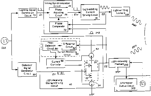
As shown in FIG. 1, the timing synchronization circuit 70 includes a
phase comparator 72 configured to a phase difference between the light-
emitting element driving signal E2 and the light-receiving element driving
signal
D2, and a phase adjusting circuit 76 configured to determine a phase shift
value
of the lighting timing signal El depending upon the phase difference output
from
the phase comparator 72. As shown in FIG. 2, the phase adjusting circuit 76 is
composed of a waveform shaping circuit 73 configured to shape the light-
emitting element driving signal E2 and the light-receiving element driving
signal
D2 respectively into rectangular waveforms, and a comparator 74 for comparing
the wave-shaped signals, and an integrator 75 configured to integrate the
output of the comparator 74 to give the phase shift value corresponding to the
phase difference between the driving signals.
The light-receiving element driving circuit 40 includes an output switch
50 which is turned on and off in response to the detection timing signal D1 to
supply a current from a DC power source 210 to the light-receiving element 200
so as to actuate the light-receiving element 200 at a timing determined by the
detection timing signal Dl. That is, the driving circuit 40 is configured such
that
the light-receiving element 200 is activated by the current from the DC power
source 210 to come into an operable condition for detection of the reflected
light
intensity. However, since the light-receiving element 200 has a capacitive
CA 02631468 2008-05-28
- 17 -
reactance, there may occur a situation where the current being fed to the
light-
receiving element 200, i.e., a current varying rate of the light-receiving
element
driving signal D2 varies in response to a considerably varying ambient
temperature, causing a delay in activating the light-receiving element 200
relative to the detection timing signal Dl. For instance, upon seeing a
considerable drop in the ambient temperature, the light-receiving element
driving signal D2, i.e. the driving current rises slowly, thereby activating
the
light-receiving element 200 with a delay relative to the detection timing
signal
Dl.
In order to eliminate the above problem, the light-receiving element
driving circuit 40 of the present embodiment is configured to include a
current
monitoring circuit 60 which monitors the current varying rate of the current
defined by the light-receiving element driving signal D2 and a current
controller
66 which regulates, based upon the output of the current monitoring circuit
60,
the current varying rate of the output current supplied from the DC power
source 210 through the output switch 50 to the light-receiving element 200,
i.e.,
the rising time of the current reaching a level for truly activating the light-
receiving element 200 as well as the falling time of the current dropping to a
level for deactivating the light-receiving element 200. The output switch 50
includes a n-type MOSFET 51 and a p-type MOSFET 52 which are connected
in series between the DC power source 210 and the ground with the light-
receiving element 200 connected between the node of the FETs and the ground.
The detection timing signal D1 is input to the gates of the FETs so as to turn
on
FET 51 and therefore supply the current from the DC power source 210 to the
light-receiving element 200 for charging the same when the detection timing
signal D1 is on, and turn on FET 52 for discharging the light-receiving
element
when the detection timing signal D1 is off. A resistor 53 is interposed
between
the DC power source 210 and FET 51 for restricting the current being fed to
the
light-receiving element 200, while a resistor 54 is interposed between FET 52
and the ground for restricting the discharging current from the light-
receiving
element.
CA 02631468 2008-05-28
- 18
The current monitoring circuit 60 includes a differential circuit 62 which
detects an instant varying rate of the light-receiving element driving signal
D2,
i.e., the current flowing through the light-receiving element 200, and a peak
detection circuit 64 which detects a maximum of the instant varying rate. The
current controller 66 is configured to control the resistors 53 and 54 for
keeping
the varying rate of the current through the light-receiving element 200 at a
predetermined value in accordance with the maximum of the varying rate output
from the peak detection circuit 64. Whereby, it is possible to give a constant
activation time for activating the light-receiving element 200 and a constant
deactivation time for deactivating the element after reception of the
detection
timing signal D1, without being influenced by the ambient temperature, thereby
improving detecting accuracy of the spatial information.
Each of the resistors 53 and 54 is made of MOSFET which varies its
on-resistance continuously in response to the gate voltage of MOSFET being
varied by the output from the current controller 66.
FIG. 5 illustrates a modification of the above embodiment which is
identical in configuration and function to the above embodiment except that a
selector 80 is provided to input a plurality of light-receiving element
driving
signals D2 selectively to the phase comparator 72 of the timing
synchronization
circuit 70. Like parts are designated by like reference numerals, and no
duplication explanation is deemed necessary.
The light-receiving element driving signals D2 are prepared
respectively from the four detection timing signals D1 to define the phase
ranges PO, P1, P2, and P3 of the intensity-modulated light. The selector 80
selects one of the light-receiving element driving signals D2 to feed the
selected
one to the phase comparator 72 in order to synchronize the light-receiving
element driving signals D2 with the light-emitting element driving signal E2.
For
instance, the first light-receiving element driving signal D2 is selected to
designate the first phase range PO during one cycle of the intensity-modulated
light, and the second light-receiving element driving signal D2 is selected
during
the next one cycle, and so on. Thus, the timing adjustment can be made over
multiplicity of the cycles by selecting the different ones of the light-
receiving
CA 02631468 2008-05-28
- 19 -
-
element driving signals D2 for different cycles. Alternatively, the selector
80
may be arranged to select random one of the four light-receiving element
driving signals D2 in consideration of that the detection of the spatial
information
requires the calculations over a number of the cycles.
(2nd Embodiment)
FIG. 6 illustrates a spatial information detection apparatus in
accordance with a second embodiment of the present invention which is
basically identical in its configuration and function to the first embodiment,
except for a supplemental phase adjusting circuit 90 which is interposed
between the detection signal generation circuit 20 and the light-receiving
element driving circuit 40 for synchronizing the detection timing signal D1
with
the light-receiving element driving signal D2. This embodiment also employs
the selector 80 having the above-described function. Like parts are designated
by like reference numerals, and no duplicate explanation is deemed necessary.
The present embodiment includes a supplemental phase comparator
92 for phase comparison between the light-receiving element driving signals D2
and the detection timing signals D1, such that the supplemental phase
adjusting
circuit 90 is responsive to the detected phase difference for preparing the
modified detection timing signals D1x and feeding them to the light-receiving
element driving circuit 40, thereby synchronizing the detection timing signals
D1
with the light-receiving element driving signals D2, and therefore feeding
thus
synchronized detection timing signals D1 to the timing synchronization circuit
70
through the selector 80. With this result, the light-emitting element driving
signal E2 is synchronized with the detection timing signals D1, i.e., the
light-
receiving element driving signals D2, enabling to keep the phase difference at
zero or predetermined value between the intensity-modulated light from the
light-emitting element 100 and the light-receiving element driving signal D2.
(3rd Embodiment)
FIG. 7 illustrates a spatial information detection apparatus in
accordance with a third embodiment of the present invention which is basically
CA 02631468 2008-05-28
- 20 -
identical in its configuration and function to the first embodiment, except
that a
timing synchronization circuit 70A is provided on a driving path side of
driving
the light-receiving element 200. Like parts are designated by like reference
numerals, and no duplicate explanation is deemed necessary.
The timing synchronization circuit 70A is interposed between the
detection signal generation circuit 20 and the light-receiving element driving
circuit 40 in order to compare the detection timing signals D1 with the light-
emitting element driving signal E2, modify the detection timing signals D1
into
modified detection timing signals D1x in accordance with the detected phase
difference, and input the modified detection timing signals D1x to the light-
receiving element driving circuit 40, thereby synchronizing the light-
receiving
element driving signals D2 with the light-emitting element driving signal E2,
i.e.,
the intensity-modulated light emitted from the light-emitting element 100. The
timing synchronization circuit 70A has the same configuration as in the first
embodiment of FIGS. 1 and 2. With this result, the light-receiving element 200
can detect the intensity of the reflected light from the object at each of the
phase ranges in exact coincidence with the phase of the intensity-modulated
light, assuring accurate detection of the spatial information. In the present
embodiment, the same selector 80 as utilized in the embodiment of FIG. 5 is
employed to select one of the four detection timing signals D1 for each of
different cycles of the intensity-modulated light, and provide the selected
signal
to the timing synchronization circuit 70A.
The timing synchronization circuit 70A includes a phase comparator
72A configured to detect a phase difference between the light-emitting element
driving signal E2 from the light-emitting element driving circuit 30 and the
detecting timing signals D1 from the detection signal generation circuit for
giving
a phase shift value corresponding to the detected phase difference and a phase
adjusting circuit 76A configured to shift the detection timing signals D1 by
the
phase shift value to modify detection timing signals D1, and output the
modified
detection timing signals D1 x.
(4th Embodiment)
CA 02631468 2008-05-28
- 21 -
_
FIG. 8 illustrates a spatial information detection apparatus in
accordance with a fourth embodiment of the present invention which is
basically
identical in its configuration and function to the third embodiment, except
that a
reference light-receiving element 110 is employed to receive the intensity-
modulated light directly from the light-emitting element 100 so as to provide
to
the timing synchronization circuit 70A an output as indicative of the cyclic
variation associated with the output from the light-emitting element driving
circuit 30. Like parts are designated by like reference numerals, and no
duplicate explanation is deemed necessary.
The reference light-receiving element 110 is disposed adjacent to the
light-emitting element 100 for receiving the intensity-modulated light
directly
from the light-emitting element 100 and outputting the co-phase signal to the
timing synchronization circuit 70A. The reference light-receiving element 110
makes the use of a portion of the CCD image sensing element realizing the
light-receiving element 200, and is oriented towards the light-emitting
element
100.
(5th Embodiment)
FIG. 9 illustrates a spatial information detection apparatus in
accordance with a fifth embodiment of the present invention which is basically
identical in its configuration and function to the third embodiment, except
for the
use of a supplemental phase adjusting circuit 90A and a supplemental phase
comparator 92A of the like configuration as in the second embodiment of FIG.
6,
in order to make phase matching between the detection timing signals D-1 and
the light-receiving element driving signals D2. Like parts are designated by
like
reference numerals, and no duplicate explanation is deemed necessary.
The supplemental phase comparator 92A is configured to compare the
phase of the modified detection timing signal D-1 x from the timing
synchronization circuit 70A with that of the light-receiving element driving
signal
D2 such that the supplemental phase adjusting circuit 90A operates to further
modify the modified detection timing signal D-I x into a further modified
detection
timing signal Dly to be output to the light-receiving element driving circuit
40,
CA 02631468 2008-05-28
- 22
thereby matching the phase of the light-receiving element driving signal D2
with
that of the modified detection timing signal D1x, i.e., the intensity-
modulated
light in synchronous therewith. With this result, it is possible to obtain the
received light intensity with regard to the phase ranges in exact coincidence
with the phase of the intensity-modulated light from the light-emitting
element
100 for improving the detection accuracy of the spatial information.
(6th Embodiment)
FIG. 10 illustrates a spatial information detection apparatus in
accordance with a sixth embodiment of the present invention which is basically
identical in its configuration and function to the third embodiment, except
that
the timing synchronization circuit 70A is configured to detect a phase
difference
between the light-receiving element driving signal D2 and the light-emitting
element driving signal E2 for modification of the detection timing signal Dl.
Like
parts are designated by like reference numerals, and no duplicate explanation
is
deemed necessary.
The timing synchronization circuit 70A determines the phase difference
between the light-emitting element driving signal E2 and the light-receiving
element driving signal D2 output from the light-receiving element driving
circuit
40 through the selector 80A, and modifies, in accordance with the phase
difference, the detection timing signal D1 into a modified detection timing
signal
D1x which is input to the light-receiving element driving circuit 40. In this
consequence, the light-receiving element driving circuit 40 prepares the light-
receiving element driving signal D2 in phase with the intensity-modulated
light
from the light-emitting element 100 in order to operate the light-receiving
element 200 in exact synchronization with the light-emitting element 100.
(7th Embodiment)
FIG. 11 illustrates a spatial information detection apparatus in
accordance with a seventh embodiment of the present invention in which a first
timing synchronization circuit 70 and a second timing synchronization circuit
70A are formed respectively in driving paths of the light-emitting element 100
CA 02631468 2008-05-28
- 23 -
and the light-receiving element 200. The configuration of the timing
synchronization circuits and the other parts are identical to the first or
sixth
embodiments. Like parts are designated by like reference numerals, and no
duplicate explanation is deemed necessary.
The first timing synchronization circuit 70 is interposed between the
lighting signal generation circuit 10 and the light-emitting element driving
circuit
30, and is composed of a first phase comparator 72 which compares the phase
of the light-emitting element driving signal E2 with that of the detection
timing
signal D1, and a first phase adjusting circuit 76 which modifies, based upon
the
=
detected phase difference, the lighting timing signal El into a modified
lighting
timing signal El x output to the light-emitting element driving circuit 30. A
selector 80 is interposed between the first phase comparator 72 and the
detection signal generation circuit 20 to output a plurality of the detection
timing
signals sequentially to first phase comparator 72, in the like fashion as in
the
embodiment of FIG. 6.
The second timing synchronization circuit 70A is interposed between
the detection signal generation circuit 20 and the light-receiving element
driving
circuit 40, and is composed of a second phase comparator 72A which
determines a phase difference between the lighting timing signal El and the
light-receiving element driving signal D2, and a second phase adjusting
circuit
76A which modifies, based upon the detected phase difference, the detection
timing signal D1 into a modified detection timing signal Dlx output to the
light-
receiving element driving circuit 40. In this embodiment, a selector 80A of
the
same configuration as that in the embodiment of FIG. 5 is utilized to select
one
of the four light-receiving element driving signals D2 for each one cycle of
the
intensity-modulated light and input the selected signal to the second phase
comparator 72A.
The two timing synchronization circuits 70 and 70A are utilized in the
present embodiment to modify the lighting timing signal El and the detection
timing signal D1 in a direction of shifting the phases thereof to come closer
from
each other, enabling to operate the light-receiving element 200 in exact phase
CA 02631468 2008-05-28
- 24
synchronization with the intensity-modulated light from the light-emitting
element 100 for improving the detection accuracy of the spatial information.
(8th Embodiment)
FIG. 12 illustrates a spatial information detection apparatus in
accordance with an eighth embodiment of the present invention which is
identical in its configuration and function to the sixth embodiment of FIG. 10
except for internal configurations of a timing synchronization circuit 70B and
the
related configurations. Like parts are designated by like reference numerals,
=
and no duplicate explanation is deemed necessary.
The timing synchronization circuit 70B includes an oscillation circuit 78
which generates a signal of which frequency varies with a varying input
voltage,
and a phase comparator 72B which detects a phase difference between the
detection timing signal D1 and the light-emitting element driving signal E2.
The
detected phase difference is fed to the oscillation circuit 78 which in turn
provides the signal which has the frequency varying based upon the phase
difference, and which is output as the modified detection timing signal D1x to
the light-receiving element driving circuit 40. With this result, the light-
receiving
element driving signal D2 comes into phase synchronization with the intensity-
modulated light from the light-emitting element 100, enabling to synchronize
the
operations of the light-emitting element 100 and the light-receiving element
200.
(9th Embodiment)
FIG. 13 illustrates a spatial information detection apparatus in
accordance with a ninth embodiment of the present invention which is identical
to the embodiment of FIG. 12 except that that the timing synchronization
circuit
70B gives an output defining the lighting timing signal. Like parts are
designated by like reference numerals, and no duplicate explanation is deemed
necessary.
The timing synchronization circuit 70B is composed of a phase
comparator 72B and an oscillation circuit 78. The phase comparator 72B is
CA 02631468 2008-05-28
- 25
configured to compare the detection timing signal D1 from the detection timing
generation circuit 20 with the light-emitting element driving signal E2 from
the
light-emitting element driving circuit 30 to provide a voltage indicative of
the
phase difference between the signals to the oscillation circuit 78. In the
present
embodiment, the oscillation circuit 78 defines the lighting signal generation
circuit and is configured to generate the lighting timing signal El output to
the
light-emitting element driving circuit 30. The oscillation circuit is provided
to
regulate the frequency of the lighting timing signal El in accordance with the
output voltage from the phase comparator 72B, and is configured to determine
the frequency of the lighting timing signal El to keep a constant phase
difference between the detection timing signal D1 detected at the phase
comparator 72B and the light-emitting element driving signal E2. The detection
timing signal D1 is fed to the phase comparator 72B through the selector 80 of
the same configuration as in the embodiment of FIG. 11.
FIG. 14 illustrates an exemplary light-receiving element driving circuit
which may be applied to the above embodiments, and is basically identical in
its
operation to the light-receiving element driving circuit 40 in the embodiment
of
FIG. 1. Like parts are designated by like reference numerals, and no duplicate
explanation is deemed necessary.
The light-receiving element driving circuit 40A includes a current
monitoring circuit 60 composed of a differential circuit 62 configured to
obtain an
instant varying rate of a light-receiving element driving current D2 flowing
through the light-receiving element 200, and a peak detection circuit 64
configured to detect a maximum of the instant varying rates obtained at the
differential circuit 62. The maximum of the varying rates detected the peak
detection circuit 64 is updated and stored in a register 68. As is discussed
with
reference to the first embodiment, the current controller 66 controls, based
upon the maximum of the current varying rate read out from the register 68,
FETs 53 and 54 acting as individual resistors in order to keep the charging
current flowing into the light-receiving element 200 from the DC power source
210 through the output switch 50 at the predetermined level, and also keep the
discharging current flowing from the light-receiving element 200 to the ground
CA 02631468 2008-05-28
- 26
through the output switch 50 at the predetermined level. With this
consequence,
it is assured to give constant rising and falling times for the charging
current and
the discharging current flowing through the light-receiving element 200 in
response to the detection timing signal D1, which enables to operate the light-
receiving element 200 free from the ambient temperature for accurate detection
of the spatial information.
The light-receiving element driving circuit 40A includes a temperature
sensor 130A for sensing the ambient temperature, a temperature table 140 for
storing the detected temperatures at a predetermined time interval, and an
activation circuit 120 connected thereto. The activation circuit 120 is
configured
to compare an instant temperature with a past temperature recorded at a
predetermined past time, and activate the differential circuit 62 and the peak
detection circuit 64 only when the temperature difference exceeds a
predetermined threshold, and otherwise deactivate the same. When the
temperature difference is below the threshold, the current controller 66
controls
the current flowing through the light-receiving element 200 based upon the
current value retrieved from the register. Consequently, it is possible to
stop the
differential circuit and the peak detection circuit within a temperature range
that
will not give an adverse effect on the operation of the light-receiving
element
200, thereby reducing the power consumption.
FIG. 15 illustrates another light-receiving element driving circuit which
may be applied to the above embodiment and is configured to modify a varying
rate of the light-receiving element driving current D2 based upon the ambient
temperature for the purpose of eliminating ambient temperature-dependent
variations in the operational response of the light-receiving element 200. The
light-receiving element driving circuit 40B includes a temperature sensor 150
for
sensing the ambient temperature, and a memory means 162 for storing
predetermined control parameters associated with the detected temperatures.
The current controller 160 reads the control parameter corresponding to the
detected temperature from the memory means 162 to apply the voltage defined
by the control parameter to the gates of FETs 53 and 54 acting respectively as
resistors for regulating the on-resistance of each FET, thereby keeping a
CA 02631468 2008-05-28
- 27
constant current varying rate of the charging current flowing into the light-
receiving element 200 from the DC power source 210 through the output switch
50 and the discharging current flowing from the light-receiving element 200 to
the ground through the output switch 50. With this consequence, it is assured
to give constant rising and falling times for the charging current and the
discharging current flowing through the light-receiving element 200, which
enables to operate the light-receiving element 200 free from the ambient
temperature for accurate detection of the spatial information.
FIG. 16 illustrates a current control scheme applicable to the above
light-receiving element driving circuit. In this instance, a plurality of DC
power
supplies 210A, 210B, and 210C are utilized to supply a current to the light-
receiving element 200 from arbitrary combination of the DC power sources,
while output switches 50A, 50B, and 50C are interposed between the
respective DC power sources and the ground. Each output switch has the
same configuration as that used in the embodiment of FIG. 1. The light-
receiving element 200 is connected between each node of the series connected
FETs 51A, 52A; 51B, 52B; 51C, 52C, and the ground. The gates of FETs
defining each output switch are connected to each other to receive the
detection
timing signal D1 simultaneously, such that FETs are turned on and off in
accordance with the detection timing signal D1 in the like manner, as in the
embodiment of FIG. 1, for charging and discharging the light-receiving element
200.
Each of the output switches 50A, 50B,and 50C is connected in series
with each of charge current controlling FETs 53A, 53B, and 53C serving as
resistors, and also with each of discharge current controlling FETs 54A, 54B,
and 54C serving as resistors. The current controller 160 activates an
arbitrary
combination of the charge current controlling FETs and the discharge current
controlling FETs to flow the current through the light-receiving element 200
at a
predetermined varying rate. The current controller 160 provides an analogue
voltage defining a current value corresponding to the predetermined varying
rate to an ND converter 164 which generates digital signals determining
respectively as to which combination of the charge current controlling FETs
53A,
CA 02631468 2008-05-28
- 28 -
_
53B, and 53C are to be turned on, and which combination of the discharge
current controlling FETs 54A, 54B, and 54C are to be turned on. The digital
signals are applied to the gates of the charge current and discharge current
controlling FETs to turn on the FETs of the designated combinations for
controlling the current flowing through the light-receiving element 200.
Thus, the plurality of the charge current controlling FETs, which are
respectively connected to the plurality of the output switches, can be turned
on
in the arbitrary combination, thereby enabling to precisely control the
charging
current to the light-receiving element 200. In this instance, the charge
current
controlling FETs 53A, 53B, and 53C are made to have equal or different on-
resistance. The same is true for the discharge current controlling FETs 54A,
54B, and 54C.
=
(10th Embodiment)
FIG. 17 illustrates a spatial information detection apparatus in
accordance with a tenth embodiment of the present invention which is identical
in its configuration and function to the embodiments of FIGS. 1 and 5except
for
the internal configuration of the timing synchronization circuit 70. Like
parts are
designated by like reference numerals, and no duplicate explanation is deemed
necessary.
The timing synchronization circuit 70 is composed of an oscillation
circuit 78 for generating a signal of which frequency varies with the input
voltage,
and a phase comparator 72 for detecting a phase difference between the
lighting timing signal El and the light-receiving element driving signal D2.
The
detected phase difference is fed in the form of a voltage signal to the
oscillation
circuit 78 which provides the signal of which frequency varies with the phase
difference, and output the signal as the modified lighting timing signal El x
to the
light-receiving element driving circuit 30. With this result, the intensity-
modulated light is emitted from the light-emitting element 100 in phase with
the
light-receiving element driving signal D2, enabling to synchronize the
operations
of the light-emitting element 100 and the light-receiving element 200.
CA 02631468 2008-05-28
- 29 -
The individual features described in each of the above embodiments
and modifications can be combined or replaced with the features of the other
embodiments and modifications, which is also within the scope of the present
invention.
Further, although the above embodiments are explained to obtain the
distance to the object within the target space as one typical spatial
information,
the present invention should not be restricted thereto and can be equally
applied to an identification of the object based upon reflectivity of the
light from
the object which is obtained through analysis of the intensity of the
intensity-
modulated light reflected from the object.