Note: Descriptions are shown in the official language in which they were submitted.
CA 02633452 2008-06-12
PCT/EP2006/069161 - 1 -
2005P22714WOUS
Circuit arrangement and method for operating a high-pressure
gas discharge lamp
Technical field
The invention relates to a circuit arrangement for operating
high-pressure gas discharge lamps. In the text which follows,
high-pressure gas discharge lamps will also be called lamps in
brief. Furthermore, the invention relates to a method for
operating such lamps. In particular, the invention deals with
avoiding acoustic resonances which may occur during the
operation of these lamps.
Prior art
Acoustic resonances are a familiar problem in the operation of
high-pressure gas discharge lamps. Depending on the geometry
and on the pressure in the lamp, these resonances occur in a
frequency range between 5 kHz and 1000 kHz and can lead to arc
irregularity and even to the destruction of the lamp in the
case of distinct resonances. Operating a lamp with an
alternating current which has a frequency in the said frequency
range is therefore not absolutely reliable.
For this reason, operating devices which operate the lamp in
the so-called square wave mode have become widely used on the
market. However, the square wave mode requires great circuit
complexity which is why there are efforts to operate the lamp
in the so-called high frequency mode in spite of the risk of
acoustic resonances. In this mode, the lamps are supplied with
an alternating current in the specified frequency range because
an operating device
CA 02633452 2008-06-12
PCT/EP2006/069161 - 2 -
2005P22714WOUS
can be implemented particularly cost-effectively especially in
this frequency range.
In the document US 2003/0111968A1 (Trestman), an operating
device is described which operates a lamp at an operating
frequency which is frequency modulated.
It is the aim of the modulation that a lamp current, at
frequencies at which the lamp has a resonance point, acts on
the lamp only so briefly that no resonance forms.
In the abovementioned prior art, the operating frequency is
modulated within a range of 50 kHz around a center frequency.
The modulation is controlled by a residual ripple of a supply
voltage. The document specified talks about a constant supply
voltage which has an actually unwanted residual ripple of, for
example, 6 Vrms which is caused by a feeding line voltage. Due
to the rectification, the residual ripple has 120 Hz at a line
frequency of 60 Hz. The lamp current thus has an operating
frequency which is modulated with a modulation frequency of
120 Hz.
The disadvantageous factor in the prior art described is that,
in spite of the modulated operating frequency, disturbing
resonance phenomena occur unless a frequency range is selected
in which the lamp only has weak resonances. The operating
frequency range covered by the modulation thus avoids frequency
ranges in which strong major resonances of the lamp to be
operated occur. The result in the prior art is that a frequency
range in which the operating frequency
CA 02633452 2008-06-12
PCT/EP2006/069161 - 3 -
2005P22714WOUS
occurs must be adapted to the lamp to be operated. The prior
art does not guarantee that two lamps which have comparable
performance data can be operated in the same frequency range.
Description of the invention
It is the object of the present invention to develop a circuit
arrangement for operating high-pressure gas discharge lamps
with modulated operating frequency in such a manner that a
flicker-free operation of the lamp is possible even when the
operating frequency covers a frequency range in which the lamp
to be operated has strong acoustic resonances.
This object is achieved by a circuit arrangement comprising an
inverter which supplies to the high-pressure gas discharge lamp
a lamp current which is essentially an alternating current with
an operating frequency which is frequency modulated in a
frequency range between a minimum frequency and a maximum
frequency, as a result of which, on the one hand, a limit mean
is defined which is equal to one half of the sum of minimum
frequency and maximum frequency and, on the other hand, an
arithmetic mean is defined which is equal to the temporal mean
of the frequency values for the operating frequency, swept in a
lamp operation, the circuit arrangement being characterized in
that the limit mean is less than the arithmetic mean.
CA 02633452 2008-06-12
PCT/EP2006/069161 - 4 -
2005P22714WOUS
The invention is based on the finding that the distinctness of
the resonance points of the lamp generally decreases with
increasing frequency, i.e., at low frequencies, it is critical
if the lamp is provided with much energy since strong
resonances can form. At high frequencies, in contrast, more
energy can be fed to the lamp since the resonances are less
distinct there. The teaching for action according to the
invention is based on this finding. In the case of a linear
modulation such as is described, e.g. in EP 1 519 637 A2
(Butler), the operating frequency increases linearly with time.
In this case, the arithmetic mean of the operating frequency
has the same value as the mean of the minimum and the maximum
frequency assumed by the operating frequency (limit mean) . No
frequency value is preferred. The energy input into the lamp is
equal at all frequency values assumed by the operating
frequency.
In the document US 2003/0111968A1 (Trestman), the modulation is
sinusoidal. The energy input into the lamp is thus no longer
equal at all frequency values. Frequency values in the vicinity
of the maximum frequency and frequency values in the vicinity
of the minimum frequency are preferred. Nevertheless, the
arithmetic mean of the operating frequency and the limit mean
are equal.
In a circuit arrangement according to the invention, the
arithmetic mean of the operating frequency is greater than the
limit mean. The consequence is that the energy is input into
the lamp preferably at higher frequency values. At low
frequency values, comparatively little energy is coupled into
the lamp as
CA 02633452 2008-06-12
PCT/EP2006/069161 - 5 -
2005P22714WOUS
a result of which the resonance points prevailing there are
only weakly excited. In this context, "weakly excited" means
that the energy absorbed by the resonant oscillation is
insufficient for producing a plasma or gas transport in the
discharge vessel. This avoids arc irregularity and thus
flickering phenomena. Frequency values which are above the
limit mean are called higher frequency values. Correspondingly,
low frequency values are below the limit mean.
In order to determine the limit mean, the mean is to be formed
from the maximum frequency and the minimum frequency according
to the above definition. In this context, the maximum frequency
is the maximum frequency value assumed by the operating
frequency due to the frequency modulation during the operation
of a lamp. Frequency values assumed by the operating frequency,
e.g. during ignition, are not taken into consideration. Neither
are frequency values which only represent fluctuations of the
operating frequency taken into consideration. At such frequency
values, no significant amount of energy is coupled into the
lamp. The frequency modulation is typically periodic with a
period in the region of 10 milliseconds. Frequency values
assumed during a period of shorter than 10 microseconds can be
considered to be fluctuations. The power spectrum of the lamp
wattage is typically rectangular, wherein the plateau of the
rectangle can also be a ramp which rises with increasing
frequency. The frequency values which limit the rectangle mark
the minimum and the maximum frequency. Frequency values which
represent fluctuations are outside the rectangle
CA 02633452 2008-06-12
PCT/EP2006/069161 - 6 -
2005P22714WOUS
and have an amplitude which is significantly below the value of
the plateau.
One aspect of the invention is providing a cost-effective
operating device with the aid of a circuit arrangement
according to the invention. Since the inventive concept can
also be implemented by means of a microcontroller, no elaborate
circuit change based on the prior art is necessary. Instead, it
may be sufficient to change the software in a microcontroller
in order to achieve stable lamp operation with the aid of the
present invention. In addition, an operating device according
to the invention is also capable of operating lamps having
different resonance points.
In general, a coupling network which has a transfer function
which describes the dependence of the amplitude of the lamp
current on the operating frequency is connected between the
inverter and the lamp. The coupling network generally has a
low-pass characteristic, i.e., at low frequencies, more energy
is fed into the lamp than at high frequencies. As a result,
especially those frequencies at which strong resonances occur
are less attenuated. The wider the frequency band in which the
operating frequency is modulated, the stronger this effect is.
A further aspect of the invention is, therefore, that the
frequency-dependence of the coupling network is compensated
for. This is advantageously achieved by a variation of the
operating frequency with time which is selected in such a
manner that the power spectrum of the power of an operated lamp
CA 02633452 2008-06-12
PCT/EP2006/069161 - 7 -
2005P22714WOUS
is uniformly distributed or increases monotonically with
frequency. The transfer function is just compensated for with
an equal distribution of the power spectrum. To shift the
energy injection into the lamp even more toward higher
frequencies, overcompensation of the transfer function can also
be implemented. The power spectrum of the power of an operated
lamp then increases monotonically with frequency.
Apart from the instability of the lamp, the frequency-
dependence of the coupling network produces a further problem.
Without compensation of this frequency-dependence, a frequency
modulation of the operating frequency causes an amplitude
modulation of the lamp current. This can lead to a flickering
of the lamp even without resonance effects. The further the
minimum frequency and the maximum frequency of the operating
frequency are apart, the more this problem will become
apparent. Particularly strong flickering phenomena can occur
from a value of 10 kHz for the difference between minimum
frequency and maximum frequency. This problem is solved by the
advantageous compensation of the transfer function described
above. An extension of the frequency range within which the
operating frequency falls is advantageous because the
proportion of energy coupled into the lamp at a discrete
frequency value then drops. If a frequency value is at a
resonance point of the lamp, less energy is supplied to a
resonance-related disturbance.
The frequency modulation of the operating frequency is
advantageously periodic with a modulation frequency. In
principle, a variation of the operating frequency with time is
also possible which can be described by noise or chaos.
CA 02633452 2008-06-12
PCT/EP2006/069161 - 8 -
2005P22714W0US
However, the implementation is then complex and switching
relief of semiconductor switches in the inverter is not always
guaranteed. The operating frequency has to change so quickly
that resonance points are only cited weakly. It is described
above what is meant by "excited weakly". Modulation frequencies
above 1 Hz are advantageous.
As described above, the implementation of the invention by
means of a microcontroller is advantageous. The variation of
the operating frequency with time is then not continuous but
only discrete frequency values occur for a respective dwell
time. The energy input into the lamp can be increased in a
frequency range by reducing the difference between two adjacent
discrete frequency values or extending the dwell time. Both
measures can also be taken at the same time. Energy injection
into the lamp in the sense of the invention is given if an
average dwell time for frequency values above the limit mean is
longer than an average dwell time for frequency values below
the limit mean.
An identical effect in the sense of the invention is given if
an average difference between two adjacent discrete frequency
values is smaller for frequency values above the limit mean
than an average difference between two adjacent discrete
frequency values for frequency values below the limit mean.
CA 02633452 2008-06-12
PCT/EP2006/069161 - 9 -
2005P22714W0US
The operating frequency is usually generated by an oscillator.
In the advantageous implementation by means of a
microcontroller, the operating frequency has in each case a
discrete frequency value. The oscillator is typically
implemented by means of a so-called timer in the
microcontroller. A control device which specifies the
respective discrete frequency value for the oscillator can also
be implemented by the microcontroller. All frequency values to
be assumed successively by the operating frequency are
advantageously stored in a storage device. The control device
or the microcontroller, respectively, reads out the frequency
values one after the other and correspondingly sets the
oscillator. The storage device can also be integrated in the
microcontroller. The control device or the microcontroller,
respectively, also controls the respective dwell time of the
oscillator at a frequency value. The dwell times for the
respective frequency values can be stored with the frequency
values in the storage device.
The transfer function can also be compensated in regulated
manner. This requires a measuring device which is suitable for
supplying the amplitude of the lamp current to the control
device. The control device is then designed in such a manner
that it selects a dwell time which increases with falling
amplitude. As a result, the oscillator dwells longer on the
frequency values which produce a relatively low amplitude of
the lamp current. In this manner, the power spectrum of the
lamp wattage can be influenced in such a manner that is equally
distributed or, if overcompensation of the transfer function is
desired, increases monotonically with frequency. Instead of
CA 02633452 2008-06-12
PCT/EP2006/069161 - 10 -
2005P22714W0US
the dwell time, the difference of adjacent discrete frequency
values can also be utilized as a control value of the control
system with the same effect.
The inverter obtains it energy from a supply voltage. The
latter, in turn, is in most cases generated from a line
voltage. In general, it is attempted to keep the supply voltage
as constant as possible since fluctuations in the supply
voltage have a direct effect on the amplitude of the output
voltage of the inverter. In particular, a so-called ripple of
the supply voltage with twice the frequency of the line voltage
is generally kept as small as possible. In contrast, an
amplitude modulation can be advantageously combined with the
present invention. With a lamp operation, the supply voltage
then has a maximum value and a minimum value. With the
difference of at least 50 V between maximum value and minimum
value, a significant compensation effect occurs.
If the variation of the supply voltage (Us) with time and the
variation of the operating frequency with time are synchronized
in such a manner that, when the operating frequency assumes its
maximum, the supply voltage also assumes its maximum, the
compensation effect is optimal. A high instantaneous value of
the supply voltage then compensates for great attenuation by
the transfer function, at least partially. The compensation
effect due to the supply voltage can be combined with the
variation of the operating frequency with time according to the
invention.
Implementation of the inverter as half-bridge is advantageous
since this is cost-effective and has a high
CA 02633452 2008-06-12
PCT/EP2006/069161 - 11 -
2005P22714WOUS
efficiency. However, other inverter topologies can also be used
such as, e.g. step-down converters, step-up converters, reverse
converters, Cuk converters.
The use of a phase-controlled full-bridge inverter is also
advantageous. Such an inverter is described in the following
document: Bill Andreycak, "Phase Shifted Zero Voltage
Transition Design Consideration and the UC3875 PWM Controller",
Unitrode Application Note U-136A, 1997. The phase control can
be used for controlling the energy which is supplied to the
lamp. This can be done in dependence on the operating frequency
so that the transfer function of the coupling network is at
least partially compensated for. This compensation can be
combined advantageously with the variation of the operating
frequency with time according to the invention.
The circuit arrangement according to the invention is
advantageously a part of an operating device for a high-
pressure gas discharge lamp. Apart from the circuit arrangement
according to the invention, the operating device can contain a
circuit for igniting the lamp, for radio interference
suppression, for safety disconnection or for other auxiliary
functions. In addition, the operating device comprises a
housing and terminals for connecting the lamp and a power
supply.
A further aspect of the invention is a method by means of which
a lamp can be operated without disturbance by acoustic
resonances and in which the power spectrum (PL) of the power of
the an operated lamp (Lp) is uniformly distributed or increases
monotonically with frequency. In the case
CA 02633452 2008-06-12
PCT/EP2006/069161 - 12 -
2005P22714WOUS
of discrete frequency values, the arithmetic mean fo is
calculated as follows:
I )
.fo-- - ~ tfntn
T n=I
It is assumed here that the operating frequency assumes a
number of N discrete frequency values fn in each case for a
dwell time tn, the N discrete frequency values fn being swept
again after the time T. T is thus the period of a modulation
frequency.
The method can also be advantageously extended as follows:
starting with a stable operation of the lamp the energy input
into the lamp is increased successively selectively at all
discrete frequency values which can be assumed by the operating
frequency, by a factor of 1.2 to 5. With a factor of less than
1.2, the effect can only be measured with difficulty, and above
5, extinction of the lamp can already occur. A device for
detecting resonance phenomena examines the lamp current or the
lamp voltage or the luminous flux of the lamp for fluctuations.
If the fluctuations exceed a predetermined limit value, the
increased energy input is set back to a value which is shorter
than 80% of the original value. If the fluctuations do not
exceed a predetermined limit value, the increased energy input
is set back to value which corresponds to the original value.
With this method, the operational reliability with respect to
resonance phenomena is increased further. Resonance points
which latently exist are recognized and
CA 02633452 2008-06-12
PCT/EP2006/069161 - 13 -
2005P22714WOUS
suppressed. The increase in energy input can be implemented in
two ways. If the dwell time at a frequency value is extended,
the energy input is also increased at this frequency. The
second way which has the same effect, of increasing the energy
input in one frequency range, consists in reducing the
difference between two adjacent frequency values.
Brief description of the drawing(s)
In the text which follows, the invention will be explained in
greater detail by means of an exemplary embodiment. In the
figures:
figure 1 shows a basic circuit diagram for a circuit
arrangement by means of which the invention can be
implemented,
figure 2 shows the variation of the operating frequency with
time of a circuit arrangement according to the
invention,
figure 3 shows the spectral power density of the lamp wattage
with DC component.
Preferred embodiment of the invention
Figure 1 shows a basic circuit diagram of a circuit arrangement
by means of which the present invention can be implemented. The
circuit arrangement has two input terminals J1 and J2 to which
a rectified line voltage can be connected. The input terminals
Jl and J2 are coupled to a PFC stage which produces a power
factor correction and provides a supply voltage Us. A storage
capacitor Cl, which is intended to buffer the supply voltage
Us, is connected in parallel with the supply voltage Us.
CA 02633452 2008-06-12
PCT/EP2006/069161 - 14 -
2005P22714W0US
A value of 4.7 microfarad has been found to be advantageous for
the storage capacitor Cl for operating a 70 W lamp. With this
value, the supply voltage attains a strong amplitude modulation
which, in combination with the present invention, can be used
for compensating for the transfer function of the coupling
network. A potential of the supply voltage is used as GND
reference potential for the circuit arrangement.
The supply voltage provides the power supply for an inverter
which is constructed as half-bridge inverter. It comprises the
series circuit of an upper and a lower switch Tl and T2 which
are connected in parallel with the supply voltage. The switches
are constructed as MOSFETs, but can also be constructed as
other semiconductor switches. The source of the upper switch T1
is connected to the drain of the lower switch at the junction
M. The control terminals of the switches, the gates of T1 and
T2 in the present case, are connected to a control device Cont.
The control device Cont is also connected to the junction M,
the supply voltage Us and the GND reference potential. The
control device Cont comprises an oscillator which generates an
operating frequency by means of which the gates of the switches
T1 and T2 are alternately driven. By this means, a rectangular
alternating voltage Uw, the amplitude of which follows the
supply voltage and corresponds to the frequency of the
operating frequency, is produced at the junction M with respect
to the GND reference potential. The alternating voltage Uw
represents the inverter output voltage of the half-bridge
inverter.
CA 02633452 2008-06-12
PCT/EP2006/069161 - 15 -
2005P22714WOUS
A series circuit consisting of a lamp choke L1 and two
capacitors C2 and C3 forms a coupling network which is
connected between the junction M and the GND reference
potential. A lamp Lp can be coupled to the capacitor C3 via
terminals J3 and J4. An ignition device which provides a high
voltage for a short time for starting the lamp is not shown.
The coupling network produces an impedance transformation from
the alternating voltage Uw to the lamp. It can also contain a
transformer. The impedance transformation of the coupling
network has a transfer function which describes the frequency-
dependence of the lamp current Il referred to the alternating
voltage Uw. In the present case, the transfer function has a
band-pass characteristic. In general, the operating frequency
is always above the resonant frequency of the transfer function
so that a reduction of the switching load on the switches S1
and S2 can be utilized. Above the resonant frequency, the
transfer function has a low-pass characteristic.
The control device Cont preferably comprises a microcontroller
and driver circuits for the switches T1 and T2. In the
microcontroller, an oscillator which generates the operating
frequency is implemented by means of software. The discrete
frequency values and their associated dwell times are stored in
the memory of the microcontroller. The software causes the
oscillator to generate an operating frequency which exhibits in
succession the stored frequency values for the stored dwell
time. Once the microcontroller has read out a last frequency
value stored, there are two possibilities
CA 02633452 2008-06-12
PCT/EP2006/069161 - 16 -
2005P22714WOUS
of proceeding: either the microcontroller begins again to read
out the frequency values with a first frequency value, or the
frequency values are now read out in a reverse order until the
first frequency value is reached again. In the first case, a
more sawtooth-shaped frequency variation is obtained with time
whereas in the second case, a more triangular frequency
variation with time is obtained. The more triangular frequency
variation has the advantage that no large jumps occur in the
operating frequency.
The pure sawtooth and triangular shape mean a linear
relationship between time and operating frequency. As a rule,
this does not correspond to the teaching of the present
invention. A nonlinear or only piecewise linear relation must
be achieved over the distance of the frequency values and/or
the dwell time. As stated above, it is important in this
context that more energy is coupled into the lamp at higher
frequencies than at low ones. The technical teaching in this
respect is the relation between limit mean and arithmetic mean
of the operating frequency stated above.
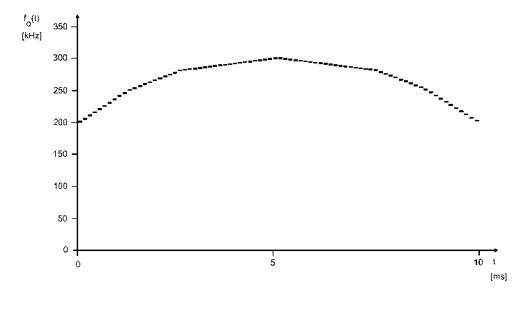
Figure 2 shows the variation of the operating frequency with
time of a circuit arrangement according to the invention. This
is a more triangular piecewise linear variation. More
triangular because the operating frequency rises for 5 ms from
a minimum frequency up to a maximum frequency and then does not
fall back immediately to the minimum frequency but drops back
to the minimum frequency during a further 5 ms. The minimum
frequency is 200 kHz and the maximum
CA 02633452 2008-06-12
PCT/EP2006/069161 - 17 -
2005P22714WOUS
frequency is 300 kHz. This results in a limit mean of 250 kHz.
The arithmetic mean is 266 kHz and is thus greater than the
limit mean, according to the invention. It is typical of a
frequency variation according to the invention that it extends
essentially at higher frequencies than is shown by the linear
connecting line between minimum frequency and maximum
frequency.
The representation in figure 2 shows that, in the exemplary
embodiment, the dwell time is approximately constant for all
frequency values. The variation with time is achieved by a
different difference between adjacent frequency values. At
frequency values close to the minimum frequency, the distances
are greater than at frequency values close to the maximum
frequency.
The variation with time repeats periodically after 10 ms. This
is no longer shown in figure 2. The periodic variation defines
a modulation frequency of 100 Hz. This modulation frequency is
clearly above 1 Hz so that discrete frequency values do not act
on the lamp for such a length of time that plasma or gas flows
are produced in the discharge vessel of the lamp. The value of
100 Hz is advantageously selected because this is the value of
the ripple frequency of the supply voltage at 50 Hz line
frequency. By this means, the amplitude modulation of the
supply voltage can compensate for the transfer function of the
coupling network in synchronism with the variation of the
operating frequency with time.
Figure 3 shows an example of the spectral power density log PL
of the power fed into the lamp Lp in a logarithmic
representation. In comparison with the spectrum of the lamp
current Il, the frequencies occurring in the power spectrum
CA 02633452 2008-06-12
PCT/EP2006/069161 - 18 -
2005P22714WOUS
are doubled. A frequency band between 360 kHz and 620 kHz
resulting from a frequency modulation of the operating
frequency between a minimum frequency of 180 kHz and a maximum
frequency of 310 kHz can be seen clearly. The power density is
essentially constant in this frequency band. This is an
advantageous consequence of the compensation for the transfer
function of the coupling network.
Between 180 kHz and 310 kHz, figure 3 shows a further frequency
band in which power is coupled into the lamp. This frequency
band is produced by a DC component which is superimposed on the
lamp current Il. This DC component is advantageously generated
by the fact that, in a half-bridge inverter, the switches do
not switch precisely symmetrically but the on-time of one
switch is in each case predominant. Due to the DC component,
the frequency range in which energy is coupled into the lamp
can be widened without widening the frequency band which is
spanned by the minimum frequency and the maximum frequency. The
amplitude of the frequency band generated by the DC component
is dependent on the value of the superimposed DC component.
In figure 3, the start of a further frequency band can be seen
which begins at 720 kHz. This frequency band is produced by the
quadrupling of the fundamental frequencies such as minimum
frequency and maximum frequency.