Note: Descriptions are shown in the official language in which they were submitted.
CA 02634511 2012-05-15
68483-52
-1-
RF RECEIVING AND TRANSMITTING APPARATUSES HAVING
A MICROSTRIP-SLOT LOG-PERIODIC ANTENNA
TECHNICAL FIELD
The present invention, in its several embodiments, relates to receiving and
transmitting apparatuses that include microstrip log-periodic antennas and,
more
particularly, to such apparatuses that include microstrip-slot log-periodic
antennas.
BACKGROUND
The present practicable range of radio frequency (RF) is approximately 10
kHz to 100 GHz, i.e., 0.01 to 100,000 MHz. Within this frequency range
electromagnetic radiation may be detected, typically by an antenna, and
amplified as
an electric current at the wave frequency. When energized via electric current
at an
RF wave frequency, an antenna may emit in the RF electromagnetic radiation at
the
RF wave frequency. Log-periodic antennas are typically characterized as having
logarithmic-periodic, electrically conducting, elements that may receive
and/or
transmit communication signals where the relative dimensions of each dipole
antenna element and the spacing between elements are logarithmically related
to the
frequency range over which the antenna operates. Log-periodic dipole antennas
may be fabricated using printed circuit boards where the elements of the
antenna are
fabricated in, conformal to, or on, a surface layer of an insulating
substrate. The
antenna elements are typically formed on a common plane of a substrate such
that
the principal beam axis, or direction of travel for the phase centers for
increasing
frequency of the antenna, is in the same direction. The antenna elements may
be
placed in electrical communication with an RF receiver and/or an RF
transmitter,
The analog and digital processing of the detected RF waveform is typically
performed by an RF receiver and the analog and digital processing of the
transmitted
RF waveform is typically performed by an RF transmitter.
CA 02634511 2012-05-15
68483-52
-2-
DISCLOSURE OF THE INVENTION
The invention in some embodiments includes radio frequency (RF)
receiving and/or transmitting systems or apparatuses having a log-periodic
antenna
having a dielectric medium such as a printed circuit board interposed between
a
microstrip log-periodic portion and a proximate slot log-periodic portion. The
perimeter of the microstrip log-periodic portion may be undersized relative to
the
perimeter of the first slot log-periodic antenna portion and a proximate
distance
between the outer perimeter of the first microstrip log-periodic antenna
portion and
the perimeter of the first slot log-periodic antenna portion, perpendicular to
the
second surface may be referenced to bound a first impedance gap. The invention
in
some embodiments may further include an antenna having a curvilinear,
electrically
conductive feed line and a substantially co-extensive curvilinear slot
transmission
line. Embodiments of the invention may further include an array of two or more
log-
periodic antennas mounted in alternating phase center orientations.
Accordingly, a
log-periodic antenna element having a layer of dielectric media interposed
between a
microstrip log-periodic portion and a slot log-periodic portion may be
disposed in an
array having two or more like elements that may be placed about vehicles, such
as
land vehicles, water vehicles and air vehicles, or mounted on stationary
structures,
such as communication towers. In addition, single or pairs of elements may be
mounted to mobile receiving, transmitting, and/or transceiving apparatuses
such as
vehicles and human-portable interface devices such as mobile telephones and
wireless personal data assistants.
According to one aspect of the present invention, there is provided a
radio frequency (RF) apparatus comprising: at least one of an RF transmitter
and an
RF receiver; an air vehicle having a fuselage and a lifting surface; and an
array of
antenna pairs conformally disposed on at least one of the fuselage and the
lifting
surface and operably coupled to the at least one of an RF transmitter and an
RF
receiver, wherein each antenna pair of the array comprises: a first log-
periodic
CA 02634511 2012-05-15
68483-52
- 2a -
antenna element having a first phase center oriented in a forward direction
relative to
the fuselage and a first slot log-periodic antenna portion in proximity to a
first
microstrip log-periodic antenna portion, and a dielectric medium interposed
therebetween; and; a second log-periodic antenna element, proximate to the
first
log-periodic antenna element, having a second phase center oriented in an aft
direction relative to the fuselage and comprising a second slot log-periodic
antenna
portion in planar proximity to a second microstrip log-periodic antenna
portion and the
dielectric medium interposed therebetween.
According to another aspect of the present invention, there is provided
a radio frequency (RF) apparatus, comprising: a communications tower having a
mast: at least one of an RF transmitter and an RF receiver; and an array of
antenna
pairs disposed circumferentially about the mast and operably coupled to the at
least
one of an RF transmitter and an RF receiver, wherein each antenna pair of the
array
comprises: a first log-periodic antenna element having a first phase center
oriented
in a first direction and a first slot log-periodic antenna portion in
proximity to a first
microstrip log-periodic antenna portion, and a dielectric medium interposed
therebetween; and; a second log-periodic antenna element, proximate to the
first log-
periodic antenna element, having a second phase center oriented in a second
direction substantially opposite the first direction and comprising a second
slot
log-periodic antenna portion in planar proximity to a second microstrip log-
periodic
antenna portion and the dielectric medium interposed therebetween.
According to still another aspect of the present invention, there is
provided a radio frequency (RF) apparatus, comprising: a human-portable user
interface unit: at least one of an RF transmitter and an RF receiver; and an
array of
antenna pairs disposed on the human-portable user interface unit and operably
coupled to the at least one of an RF transmitter and an RF receiver, wherein
each
antenna pair of the array comprises: a first log-periodic antenna element
having a
first phase center oriented in a first direction and a first slot log-periodic
antenna
portion in proximity to a first microstrip log-periodic antenna portion, and a
dielectric
CA 02634511 2012-05-15
68483-52
-2b-
medium interposed therebetween; and; a second log-periodic antenna element,
proximate to the first log-periodic antenna element, having a second phase
center
oriented in a second direction substantially opposite the first direction and
comprising
a second slot log-periodic antenna portion in planar proximity to a second
microstrip
log-periodic antenna portion and the dielectric medium interposed
therebetween.
DESCRIPTION OF THE DRAWINGS
Reference is now made to the following description taken in conjunction
with the accompanying drawings, in which:
FIG. 1 illustrates in plan view an example element of the printed circuit
and transmission line characteristics of the microstrip line log-periodic
array feed side
of the present invention;
FIG. 2 illustrates in plan view an example of the ground side of the log-
periodic slot array of the present invention;
CA 02634511 2008-06-09
-3-
FIG. 3A illustrates in a plan view an example of six elements in the example
array of the microstrip log-periodic feed side of the slot array aligned with
the
log-periodic ground side of the slot array;
FIG. 3B illustrates in a cross-sectional view an example of an element in the
example array of the microstrip log-periodic feed side of the slot array
aligned with
the log-periodic ground side of the slot array;
FIG. 4 illustrates in plan view an exemplary, typical placement of two
antenna elements of the present invention proximate to one another and
oriented so
that each has a traveling phase center verses frequency opposite the other;
FIG. 5A illustrates in plan view an exemplary, typical embodiment where a
printed circuit board has two microstrip log-periodic array feeds on a top
side and
their corresponding aligned ground planes on the opposite side of the printed
circuit
board;
FIG. 5B illustrates in a cross-sectional view the fork region of a tongue of
an
embodiment engaging a coax inner wire;
FIG. 6 illustrates in a cross-sectional view an exemplary mounting;
FIG. 7 illustrates in plan view an exemplary curved taper in the grounded
side of the exemplary microstrip log-periodic array from the last element to
the
ground plane;
FIG. 8A illustrates in plan view an exemplary microstrip feed line as it
curves from the feed-line tongue to the base of the exemplary microstrip
log-periodic array;
FIG. 8B illustrates in cross-sectional view an exemplary microstrip feed line
as it curves from the feed-line tongue to the base of the exemplary microstrip
log-periodic array;
FIG. 9 illustrates an exemplary antenna gain pattern produced from
measurements of an exemplary antenna taken at a low frequency;
FIG. 10 illustrates an exemplary antenna gain pattern produced from
measurements taken at a midrange frequency;
FIG. 11A illustrates an exemplary receiver system operably connected to
exemplary antenna element embodiments of the present invention;
CA 02634511 2008-06-09
-4-
FIG. 11B illustrates an exemplary transceiver system operably connected to
exemplary antenna element embodiments of the present invention;
FIG. 12 illustrates an exemplary conformal antenna array disposed about a
support structure;
FIG. 13 illustrates an exemplary conformal antenna array mounted to
portions of an air vehicle;
FIG. 14A illustrates an exemplary system where an array of exemplary
antenna elements is disposed about a portion of a communications tower and in
communication with mobile apparatuses; and
FIG. 14B illustrates an exemplary arrangement of exemplary antenna
elements for integrating with the exemplary mobile apparatuses.
As used herein, the term "exemplary" means by way of example and to
facilitate the understanding of the reader, and does not indicate any
particular
preference for a particular element, feature, configuration or sequence.
MODE(S) FOR CARRYING OUT THE INVENTION
The present invention, in its several embodiments, include a log-periodic
antenna having microstrip slot elements on a first, or top, side of a
dielectric medium
and a slot ground plane of the elements on a second, or bottom, side of the
dielectric
medium, where the radiating elements are oriented with alternating and
opposing
phases, e.g., 180 degrees phase differences, and where the combination may
operate
as a broadband log-periodic antenna. In addition, the present invention in its
several
embodiments may have a grounded modified semi-coplanar
waveguide-to-microstrip line transition. The feed input of some embodiments
typically has a transition from an unbalanced microstrip transmission line and
may
have a microstrip feed transmission line tapering from a base microstrip slot
dipole
element on a top side of the dielectric medium and a slotted ground plane
under the
transmission line tapering from the primary slot dipole element in a ground
plane
medium on the bottom side of the dielectric medium. Exemplary embodiments of
the microstrip transmission line have a primary conductor strip in voltage
opposition
to a reference ground plane with an interceding dielectric between the two
conductors. For example, the element embodiment may be fed by two slot lines
in
CA 02634511 2008-06-09
-5-
parallel that have as a common potential a main conductor. The main conductor
typically tapers to a width that sets the impedance of the microstrip
transmission line
and along the same length, a void or slot in the ground plane is tapered to a
zero
width or corner point. In some embodiments, these tapered regions operate to
transition the field line from being substantially between the microstrip
conductor
and the ground plane as in a capacitor, to being substantially fringing fields
between
the edges of the conductors passing through the dielectric.
Exemplary array embodiments of the present invention typically include an
array of at least a pair of substantially frequency-independent planar antenna
array
elements where the first member of the pair of antenna array elements has a
phase
center axis substantially opposite in direction to the phase center axis of
the second
member of the pair of antenna array elements. The antenna element patterns may
be
aligned, i.e., top plan-form relative to bottom plan-form, which forms a
microstrip
log-periodic array (MSLPA) having a principal axis. Each MSLPA typically
includes a slot transmission line running along the principal axis of the
MSLPA that
may function as feeds for the slot dipole elements the typically trapezoidal
elements
emanating in bilateral symmetry from the transmission line. In some
embodiments,
parasitic, or center, microstrip lines or slots may be interposed within the
regions
formed by the dipole elements and the transmission line of the combined
layers.
The outer perimeter of the feed side of the MSLPA typically describes a
pattern or
plan-form, the ground plane side of the log-periodic slot array typically then
covers
a pattern of the perimeter of each feed side microstrip line element of the
top side
and along with some additional width at substantially perpendicular to the
perimeter
to establish an impedance slot.
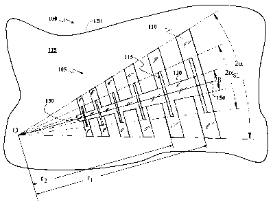
FIG. 1 illustrates an exemplary microstrip dipole element array and
transmission line characteristics of a microstrip log-periodic array
embodiment 100
of the present invention that is typically affixed on a first or top surface
125, or front
side, of a dielectric medium 120, such as a printed circuit board. The
transmission
line portion 130 of the exemplary array is within the region subtended by the
angle 20. The log-periodic array of the exemplary embodiment is typically
symmetric in a plane about a principal axis 150 where the dipole elements
extend as
trapezoidal portions bounded, in this example, by the angle 2a. Generally, an
CA 02634511 2008-06-09
-6-
internal centered slot 115 is provided by the pattern of the microstrip line
at each
element and may cross or traverse the transmission line portion 130. The
pattern of
the microstrip portion 105 of the MSLPA 100 may be a thin metallic film and
the
internal centered slot 115 may be fashioned by a trapezoidal region absent of
the
metallic film. The transverse extent of each interior slot, in this example,
is bounded
by the angle 2a SL. For purposes of illustrating the proportions of the
microstrip
elements of the antenna, the dipole elements, or dipole teeth of the array
that may
traverse transmission line portion are numbered starting with the dipole of
largest
wavelength. For example, the first dipole 110 is shown with the longest span,
i.e.,
the longest portion traversing the transmission line portion 130. The
exemplary
minimal radial distance from the reference origin, 0, for the microstrip
portion of
the first dipole element may be represented as rl and the minimal radial
distance for
the second dipole element may be represented as r2.
FIG. 2 illustrates an exemplary ground plane side 210 of the microstrip
log-periodic slot array (MLPSA) 100 of the present invention where a slot
log-periodic antenna portion 200 may be typically formed from a metallic
ground
plane which may be applied as the bottom or second surface, of the interposed
medium, such as a printed circuit board, and may form the back, bottom or
opposite
side, of the printed circuit board, i.e., opposite the feed side where the
microstrip
portion 105 of the MLSPA 100 is affixed. The feeder transmission line portion
of
the array is within the region that may be shown as subtended by the angle 20
plus
twice the planar slot width, shown as a small angle, 5, and typically a
distance
perpendicular to the local perimeter, w (not shown in FIG. 2). The slot width
is
typically adjusted in the matching of the impedance of the array of elements,
both
the microstrip elements and the slot elements of the ground plane, and
including the
interposed printed circuit board or other mounting media. Typically, the
log-periodic array of the present invention is substantially symmetric in
plane about
a principal axis 250 where the slot dipole elements traverse a slot
transmission line
230 and extend as trapezoids bounded by the angle 2a plus twice the slot
width, w,
represented as a small angle, 25 as above.
For purposes of illustrating the slot portions of the MLPSA 200, the elements
of the array are numbered starting with the slot dipole element of largest
CA 02634511 2008-06-09
-7-
wavelength 220, that is, the element having the exemplary largest transverse
span.
The maximal radial distance from the reference origin, 0, for the first dipole
may be
represented as R1. The maximal radial distance from the reference origin, 0,
for the
second dipole may be represented as R2. The minimal distance from the
reference
origin, 0, for the first dipole may be represented as r1 less the impedance
slot width.
A similar relationship may be made for R2 and r2. Typically, the feeder
transmission
line angle of the microstrip, or top portion 20 is smaller than the angle of
2/3 plus the
angle increment, e.g., 23, required for impedance slot width of the ground
side of the
dielectric medium, and likewise the angle 2a bottom plus the angle increments
23 of
the ground side required for impedance slot width is greater than 2a of the
top side.
Rather than expressed by the angle, 3, this may be expressed as the linear
distance,
w, when viewing the planar projections of the microstrip dipole elements and
the
slot dipole elements in plan view.
For each exemplary pair of top and bottom trapezoidal dipole elements, an
impedance slot may be created as shown in the top view of the antenna of FIG.
3A,
where FIG. 3A illustrates in a top view an exemplary array of the MSLPA
showing
six element pairs and where the impedance slot is shown in the space 310
between
the microstrip and the ground plane having, in a projection made substantially
perpendicular to the local surface and through the interposed dielectric media
120,
the slot width 311, w. In this exemplary array of the MSLPA, the top and
bottom
sides are overlaid, where the dashed lines indicate the boundary or slot
perimeter of
the ground-side present on the bottom side of the dielectric medium.
Accordingly,
in an exemplary embodiment, the MSLPA is affixed to the dielectric medium,
such
as a printed circuit board (PCB), in an orientation such that the edges of the
ground
plane side of the slots of the MLPSA generally provide for an outer perimeter.
Put
another way, the perimeter of the slot portion is oversized relative to the
perimeter of
the microstrip portion and the perimeter of the microstrip portion is
undersized
relative to the slot portion. FIG. 3B illustrates in cross-sectional view the
microstrip
portion 110 of an element in relation to a ground plane portion 210 and an
interposed PCB, as an example of a dielectric medium 120. In this view (FIG.
3B),
an internal centered slot 115 may be seen in cross-section as well as a slot
element 220 of the MLPSA. Also illustrated in cross-sectional view of FIG. 3B,
the
CA 02634511 2008-06-09
-8-
impedance slot is shown in the space 310 between the microstrip and the ground
plane having, in a planar projection, the slot width 311, w. The resulting
stacked
MSLPA is operable to function as a substantially frequency-independent antenna
having a traversing of its center with respect to frequency substantially
along the line
of bilateral symmetry 350 (FIG. 3A).
Another antenna embodiment is described as follows where w represents the
planar width of the impedance slot, r represents the element expansion ratio,
and c
represents a measure of tooth width in the following equations:
Rn+1 = rn+i [1]
Rn rn
and
= Yn [2]
Rn
The "over angle" subtended by the completed antenna may be represented 2a
+ 26. Exemplary relationships include an c of , a 0 of asl/3, and an aSL of (a
+
6/2.
Exemplary antenna array properties include a value for an over angle, or 2a
+ 25 of approximately 36 degrees, a value for 2a of approximately 33 degrees,
a
value for 2aSL of approximately 18 degrees, and a value for 2/3 of
approximately 6
degrees.
Exemplary antenna array properties are illustrated in Table 1 with distances
in centimeters for dipole teeth numbered 1-19:
CA 02634511 2008-06-09
-9-
TABLE 1
Exemplary Antenna Properties
R r T e w #
13.970 12.649 0.82 0.91 0.220 1
11.455 10.373 0.82 0.91 0.180 2
9.393 8.506 0.82 0.91 0.148 3
7.704 6.975 0.82 0.91 0.121 4
6.317 5.720 0.82 0.91 0.099 5
5.179 4.689 0.82 0.91 0.082 6
4.247 3.846 0.82 0.91 0.067 7
3.482 3.155 0.82 0.91 0.055 8
2.855 2.586 0.82 0.91 0.045 9
2.342 2.121 0.82 0.91 0.037 10
1.920 1.740 0.82 0.91 0.030 11
1.575 1.425 0.82 0.91 0.025 12
1.290 1.168 0.82 0.91 0.020 13
1.059 0.958 0.82 0.91 0.017 14
0.869 0.787 0.82 0.91 0.017 15
0.711 0.645 0.82 0.91 0.013 16
0.584 0.513 0.77 0.88 0.012 17
0.450 0.394 0.77 0.88 0.009 18
0.345 0.305 0.77 0.88 0.007 19
The present invention, in its several embodiments, typically has the antenna
structurally divided into two portions on either side of a mounting medium,
such as
a two-sided PCB. The two-sided printed circuit board embodiment accommodates
the exemplary feed described below. That is, the feed transition from
microstrip to
the radiating elements may be fabricated with a dielectric medium, such as a
two-sided printed circuit board and a tapered ground. In addition to the
various feed
CA 02634511 2008-06-09
-10-
embodiments, the two-sided PCB structure and material provide additional means
by
which the antenna impedance of the several antenna embodiments may be
controlled, for example, by variation of material thickness and by selection
of the
dielectric constant of the PCB. Due to the field constraint within the
dielectric
material, high power, high frequency alternative embodiments of the present
invention may exploit the increased breakdown characteristics of the higher
frequency, i.e., the smaller wavelength, portion of the antennas.
FIG. 4 illustrates an exemplary placement of two microstrip, log-periodic
arrays of an embodiment of the present invention that are proximate to one
another
and oriented so that the phase center 415 of a first antenna 410 is
substantially
opposite the phase center 425 of the second antenna 420 and may receive or
transmit
substantially as a single combined antenna element. These opposing phase
centers
are typically offset, which may adapt these combined elements to the direction
finding of targets out of the plane of the elements; that is, receiving RF
energy at
angles of arrival substantially off the axes 415 and 425 of the opposing phase
centers.
FIG. 5A illustrates an exemplary embodiment 500 where the PCB has two
MSLPAs with their feeds on the illustrated upper surface, or top side, and
their
corresponding aligned ground planes on the opposite surface, or bottom side,
of the
PCB where each form an antenna and together form an antenna array on the PCB.
FIG. 5A illustrates exemplary feed tongues 510 and a second feed tongue 520,
i.e.,
one for each antenna. For example, the inner wire or conductor 523 of a
coaxial
feed line, once within the fork 511 or 521 of each feed tongue, may be
soldered or
otherwise put in electrical connectivity with the microstrip feed line 512,
522 and
soldered or otherwise put in electrical connectivity with the ground plane. As
illustrated by FIG. 5B, a cross-sectional view of FIG. 5A at the second tongue
520,
typically, the outer conductor 524 of the coaxial conductor may also have
direct
current (DC) connectivity with the ground plane 210, which is shown by example
as
being on the bottom side of the PCB 120, and the inner wire 523 also typically
has
connectivity with the microstrip feed line 522 which is shown by example as
being
on the top side of the PCB 120. Further detail of the planar projection of the
perimeter of an exemplary curvilinear portion of the microstrip feed line
relative to
CA 02634511 2008-06-09
-11-
the planar projection of the perimeter of an exemplary curvilinear, tapered
ground
transition is described below and illustrated in FIG. 8A.
Mounting
The antenna array elements of the several embodiments may be mounted
above a grounded cavity, or other receiving element, that provides both
grounding
and feed lines such as the coaxial conductor example described above.
Illustrated in
FIG. 6 is an exemplary cavity having a bottom surface 610 that may be formed
of
metal, e.g., steel, titanium, aluminum or various metal alloys, where a radio
frequency absorber element 620, or sheet, may be interposed between the cavity
surface and the bottom side such as the ground plane 210 of the antenna array
elements. In addition, a low dielectric material deployed as foam or a
honeycomb-type element 630 that may be interposed between the radio frequency
absorber element 620 and the bottom side 210 of the antenna array elements.
The antenna array element 100, an absorber layer element 620, and a low
dielectric element may be bonded together. For environmentally challenging
environments, such as for example those encountered in moisture laden
atmosphere
with high dynamic pressures experienced at supersonic velocities, a cover 640,
skin,
or radome may be used to shield, or protect, or otherwise cover all or a
portion of the
top 125 or outwardly directed portion of the antenna array element, a covered
portion that may include the top side 125 of the dielectric material 120,
thereby
covering a region that could or would otherwise be in direct environmental
contact
with free space, for example. The microstrip line array of the top side and
the
ground plane slots of the bottom side of the array may be fabricated on a low
loss,
low dielectric substrate, e.g., RT5880 DUROID (TM), a substrate available from
Rogers Corporation, Advanced Circuit Materials, of Chandler, Arizona, or may
be
fabricated of equivalently low dielectric materials at thickness of around 15
mils, for
example. Other thickness ranges may be used depending on the properties of the
low dielectric material and the desired gap 310 (FIG 3B). In addition, a
cavity
resonance absorber, such as a flexible, ferrite-loaded, electrically non-
conductive
silicone sheet may be applied within a cavity mounting. Where the cavity is
formed
of metal or has a metalized or electrically conductive surface, the antenna
array may
CA 02634511 2008-06-09
-12-
be in electrical contact with the cavity surface where the cavity surface may
serve as
the base ground plane of the antenna array. In addition, the two-sided PCB
embodiments of the array may provide the ability to control, by selection, the
impedance by selecting from variations of PCB material thickness and their
respective dielectric constants.
The substantially planar profile of the antenna array may exhibit some
curvature and, whether flat or contoured, may be conformally mounted. In those
geometries requiring conformal mounting about a radius of curvature, the
transverse
edges of the otherwise typically trapezoidal dipole elements are themselves
typically
curved to accommodate a curved printed circuit board surface that may then
conform to a selected mounting geometry.
The several embodiments of the invention have gain and pattern properties,
which are typically robust with respect to the effect of cavity depth on the
elements.
For example, a cavity with an absorber-lined bottom surface and metal back
negligibly affects on the antenna gain and pattern properties where cavity
depth is at
a minimum of 0.1 lambda, i.e., one-tenth of a wavelength of the frequency in
question. Put another way, the exemplary embodiments may be configured to
experience a slight loss of antenna gain or antenna gain-angle pattern
distortion for
cavities shorter than one-tenth lambda with a corresponding change in the
input
voltage standing wave ratio (VSWR).
Microstrip Feed Structure
Some high power, high frequency applications of the several embodiments
may experience an increase in the breakdown characteristics of the high
frequency
portion of the elements. The exemplary feed structure embodiments readily
accommodate elements operating from frequencies below X-band through well into
the Ka-band. In order to accommodate structures into the upper Ka-band,
micro-etching techniques are typically applied. At these higher frequencies,
material thicknesses are typically reduced from those accommodating X-band
antenna embodiments.
Each of the antenna array elements typically includes a microstrip feed
structure that splits and feeds to the two-sided antenna array element. Some
CA 02634511 2008-06-09
-13-
embodiments of the feed structure combine microstrip feed lines with a tapered
ground transition and the two-sided antenna element. Typically the feed
structure
includes a microstrip feed line having a tapered ground transition. FIG. 7
illustrates
an exemplary curvilinear, tapered ground transition 710 from the last element
(e.g., a
high or highest frequency element) of the MSLPA. The transition from the last
slot
element 720 to the feed transmission line is tapered in this exemplary fashion
in part
to minimize VSWR effects and to continue the transition from microstrip to the
antenna element. The feed transmission line is tapered in this exemplary
embodiment to a point 740. In addition, the base of the slot feed transmission
line
taper may curve in the direction of the exemplary feed-line tongue 510, 520 to
minimize sharp angles that may otherwise set up what may be undesired or
parasitic
active portions.
FIG. 8A illustrates the exemplary microstrip feed line 810 as it curves from
the feed line tongue 510 to the base of the MSLPA 820 where the feed line
flares out
to the last element of the MSLPA. The last element 830 is tapered, in this
example,
in part to minimize feed point radiation and prevent the last element from
arraying
with the proximate element to form a radiating beam for this section and
accordingly
improve input matching over base elements lacking a tapered feed line. The
tapering, or decreasing width, of the transition from the last slot element
720 to the
slot feed transmission line 710 may cause the slot width or perimeter of the
slot feed
transmission line, in a planar projection made perpendicular or substantially
perpendicular to the surface or local surface regions of the dielectric medium
120 to
which the slotted ground plane 210 is attached, to fall within, as depicted at
850, the
plan form of the exemplary microstrip feed line 810 that is to be within a
projection
of the perimeter of the microstrip feed line 810 made perpendicular to the
surface or
local surface regions of the dielectric medium 120 to which the microstrip
feed line
810 is attached. The last element in these exemplary embodiments typically
does
not have a parasitic slot within its perimeter. Also shown in this view is the
relative
orientation of the exemplary microstrip feed line 810 and the curvilinear,
tapered
ground transition 710 along with its exemplary tip ending 740 that, in a
planar
projection made planar to the local surface, is within the plan form, or
perimeter, of
the exemplary microstrip feed line 810; that is, within a projection of the
exemplary
CA 02634511 2008-06-09
-14-
microstrip feed line 810 made perpendicular to the local surface. Accordingly,
when
viewed in plan view and projecting across the interposed dielectric medium
120, the
antenna embodiments may have a curvilinear, electrically conductive feed line
810
and a substantially co-extensive curvilinear slot transmission line 710 for a
portion
of the run of the microstrip feed line 810. FIG. 8B illustrates in cross-
sectional
view, the exemplary microstrip feed line 810 as it curves from the feed line
tongue 510 to the base of the MSLPA 820 where the feed line flares out to the
last
element of the MSLPA 830. Also illustrated in this view is the tapered ground
transition 710 ending at the tip corner 840.
Receiving, Transmitting and Transceiving
The antenna array embodiments of the present invention may provide
substantially constant forward directivity, typically with only subtle or
otherwise
operationally negligible changes in beam-width, and afford an antenna array of
forward and aft facing elements of equal or nearly equal performance. For
purposes
of illustrating the performance of an embodiment of the present invention, the
antenna array of forward-oriented and aft-oriented element arrays where the
MSLPAs have fifteen trapezoidal dipole elements, i.e., teeth, and one base
tapered
trapezoidal dipole element were tested. FIG. 9 illustrates an antenna gain
pattern 900, in dB, as a function of beam angle pattern produced from
measurements
taken at a low frequency, i.e., directed radio frequencies intended to excite
the larger
dipole elements. FIG. 10 illustrates an antenna gain pattern 1000, in dB, as a
function of beam angle produced from measurements taken at a midrange
frequency,
i.e., directed radio frequencies intended to excite the intermediate-sized
dipole
elements.
The antenna pairs 500 (FIG. 5A) may be mounted, as arrays of pairs, to
surfaces that may include surfaces integral to vehicles, such as air vehicles
and
surface portions of sensor pods that may be deployed on vehicles such, as air
vehicles.
The antenna element embodiments are suitable for conformal mounting, for
example, structures shaped principally for low drag properties such as those
shapes
found in air vehicles and land and marine vehicles having application
sensitive to
CA 02634511 2008-06-09
-15-
dynamic pressure conditions and disruptions of laminar flow patterns.
Accordingly,
an exemplary mounting site for one or more antenna elements may be a portion
of a
rocket or missile. The cylindrical shape of the body would allow for a
circumferential array of elements of fore and aft configuration. With
excellent low
angle pattern coverage the system could achieve near full hemispheric
coverage.
Such a system can provide direction finding (DF) and angle-of-arrival (AOA)
input
signals. For some broad side angles it also provides additional benefit in AOA
and
DF in that there are twice as many elements with opposing phase directions
that
have a view of the incoming signal. A single forward looking set maybe
implemented for a forward-only array for DF/AOA applications. A single forward
looking set would simply have limited the total field of view compared with a
forward and rear-looking embodiment.
The antenna elements may be electrically connected to a radio frequency
receiver system or a radio frequency transmitting and receiving system which
may
be termed a transceiver. An RF receiver may process the electric current from
the
antennas via a low noise amplifier (LNA) and may then down convert the
frequency
of the waveform via a local oscillator and mixer and may process the resulting
intermediate frequency waveform via an adaptive gain control amplifier
circuit. The
resulting conditioned waveform may be sampled via an analog-to-digital
converter
(ADC) with the discrete waveform being processed via a digital signal
processing
module. Where the frequency of the RF waveform is well within the sampling
frequency of the conversion rate of the ADC, direct conversion maybe employed
and the discrete waveform may be processed at a rate comparable to the ADC
rate.
Receivers may further include signal processing and/or control logic via
digital
processing modules having a microprocessor, addressable memory, and machine
executable instructions. An RF transmitter may process digital waveforms that
have
been converted to analog waveforms via a digital-to-analog converter (DAC) and
may up-convert the analog waveform via an in-phase/quadrature (FQ) modulator
and/or step up the waveform frequency via a local oscillator and mixer, then
amplify
the up-converted waveform via a high-power amplifier (HPA) and conduct the
amplified waveform as electric current to the antenna. Transmitters may
further
include signal processing and/or control logic via digital processing modules
having
CA 02634511 2008-06-09
-16-
a microprocessor, addressable memory, and machine executable instructions.
Transceivers generally have the functionality of both a receiver and a
transmitter,
typically share a component or an analog or digital signal processing module,
and
employ signal processing and/or control logic via digital processing modules
having
a microprocessor, addressable memory, and machine executable instructions.
FIG. 11A illustrates in a functional block diagram that as part of a receiver
system 1100, the RF energy sensed by the exemplary antenna elements 1111, 1112
of an antenna array 1110 may be processed within a receiver subsystem 1101 via
switches, low noise amplifiers, bandpass filters and/or other signal
conditioning
processes and filters and may be stepped down, i.e., down converted, in
frequency
for further processing by the digital signal processing 1102 of the receiver
and
associated digital signal processing. FIG. 11B illustrates in a functional
block
diagram that as part of a transceiver system 1150 having an RF receiving, or
receiver, subsystem 1151 and an RF transmitting, or transceiver, subsystem
1152,
the exemplary antenna elements 1161, 1162 of an antenna array 1160 may be
energized, via one or more properly thrown switches 1153 to transmit signals
initiated by the digital signal processing 1154 and conditioned by the
transmitting
subsystem 1155 and, when not transmitting, the exemplary antenna elements may
function as passive elements to sense incoming RF energy that this is
conducted,
again via one or more properly thrown switches 1153 to the RF receiver
system 1151. An RF transmitting system, whether a transceiver subsystem or a
separate transmitter system, functions separately at the front-end (i.e.,
proximate to
the antennas) from the receiver and so the transmitter antennas and receiver
antennas
may be physically different antennas or time-shared via switches. Accordingly,
references to an RF transmitter refer generally to the transmitting
functionality
whether embodied as a stand-alone transmitter or a transmitter subsystem of a
transceiver. Likewise, references to an RF receiver refer generally to the
receiving
functionality whether embodied as a stand-alone receiver or a receiver
subsystem of
a transceiver.
FIG. 12 illustrates an array of antenna pairs 1210, where each pair 500 has an
alternating forward-directed phase center 415 and aft-directed phase center
425, and
each pair 500 is disposed substantially equidistantly about a centerline 1220
of a
CA 02634511 2008-06-09
-17-
mounting structure 1200, itself having a surface 1205 that may form a portion
of the
fuselage or other surface of an air vehicle.
While cylindrical or round embodiments of an array of antenna elements or
pairs of elements have been shown in the example of an air vehicle fuselage,
these
elements, of one or various scales, may be applied to oval, rectangular and
multisided structures, such as hexagons and octagons. Antenna elements, of one
or
various scales, may also be embedded into surfaces of wings along an axis
rather
than or in addition to an array disposed circumferentially about the fuselage.
Multiple elements can be separated by a wing or fuselage, exemplified by
separation
on the top and bottom of a wing or on the left and right wings, or on the
vertical fins
of an aircraft or missile. FIG. 13 illustrates the mounting structure 1200
placed at
the forward of end of the fuselage 1310 and, in this example, placed aft of a
nose
cone or radome 1320. The mounting structure has an array of antenna pairs
1110,
placed at the front end of an exemplary air vehicle 1300 which may then
cooperatively function as a mobile receiving or transmitting apparatus. The
array of
antenna pairs 1210 is typically covered by a protective covering 640 when the
mounting structure is placed in proximity to the front end of an air vehicle
1300.
The front end portion of the fuselage 1310 having an MSLPA 100 (FIG. 3A), an
antenna pair 500, or an array of antenna pairs 1210 may comprise a guidance
section 1330 of the air vehicle 1300. The guidance section 1330 may further
include
the nose cone or radome 1320. Also shown is a linear array of antenna pairs
1350
mounted conformally on a lifting surface 1360 of the air vehicle 1300.
Some antenna embodiments of the present invention may be used to send,
receive or transceiver RF signals. Accordingly, an array of at least a pair of
substantially frequency independent planar antenna array elements may function
as a
receiving array and may alternatively function as a transmitting array or a
transmitting and receiving, that is, the array may function as a transceiver
array.
Scaled Embodiments
Because of the feed structure, the bandwidth capabilities are extremely
broad. A scaled version of the prototype antenna was created at one-seventh
(1/7) of
the original size. Properties of an exemplary antenna scaled from the example
CA 02634511 2008-06-09
-18-
antenna of Table 1 are provided in Table 2 with distances in centimeters for
dipole
teeth numbered 1-9:
TABLE 2
Exemplary Antenna Properties
R r E w #
1.920 1.740 0.82 0.91 0.030 1
1.575 1.425 0.82 0.91 0.025 2
1.290 1.168 0.82 0.91 0.020 3
1.059 0.958 0.82 0.91 0.017 4
0.869 0.787 0.82 0.91 0.017 5
0.711 0.645 0.82 0.91 0.013 6
0.584 0.528 0.82 0.91 0.009 7
0.478 0.434 0.82 0.91 0.008 8
0.394 0.356 0.82 0.91 0.006 9
Dielectric thickness was also partially scaled down from the antenna element
characterized in Table 1, but, due to material limitations, was not fully
scaled down.
The one-seventh scaled antenna element characterized by Table 2 has only
one-quarter (1/4), rather than a one-seventh, of the dielectric thickness of
the antenna
element characterized in Table 1. So, if RT5880 DUROID (TM) is used as a
substrate, the scaled thickness of the antenna element characterized in Table
2 is
approximately 4 mils. Overall, the scaling resulted in the antenna element
characterized in part by Table 2 operating at seven times the frequency of the
antenna characterized in part by Table 1, and the scaled antenna element was
tested
to the frequency limit of the network analyzers supporting the test
conditions. The
feed structure continued to operate to the analyzer upper limit which is more
than
double the frequency of the full scale element example of Table 1. Being
readily
scalable, the various scaled embodiments of the exemplary antenna maybe
applied
to a variety of structures due in part to their functioning at the various
scaled sizes.
CA 02634511 2008-06-09
-19-
In telecommunication applications, the extreme bandwidth and opposing
phase travel of pairs of elements support systems such as cellular base
stations or
point-to-point communication systems. Typical cellular system frequencies
range
from 800MHz to 2GHz in the United States, or as high as 3.4 GHz abroad. This
extreme bandwidth provides a diversity antenna system to allow switching to
the
strongest signal and yet provide attenuation to other towers limiting tower
interference and reducing tower traffic. From a mobile unit side, an antenna
element, pair of elements, or array of elements or array of elements pairs may
be
conformally mounted into the top surface of a vehicle such as a car or truck.
One
antenna could allow for coverage of all cellular systems in a single element.
From
the tower side, an annular or circular-shaped array may provide DF/AOA
tracking of
subscribers for system traffic control or to enhance E911 capabilities of the
overall
system. Exemplary telecommunication embodiments may exhibit particular
applicability when considering phones or communication appliances that do not
include a GPS tracking capability or where the GPS quality is attenuated due
to
partial or complete satellite line-of-sight blockage. FIG. 14A illustrates a
mobile
communication system 1400 comprising a communication tower 1402, a
handset 1404, or human-portable user communication interface, having, for
example, one or a pair of conformally embedded exemplary antenna elements 1430
(not shown) and a transceiver, and the system may further comprise a vehicle
1406
also having a pair of exemplary antenna elements 1430 and a transceiver (not
shown). The mobile communication system 1400 may further comprise a mobile
communications platform functioning similarly to the stationary communications
tower 1402 and may further include air vehicles 1300 (see FIG. 13). The
handset 1404 may include a human auditory interface for speaking and listening
and
may include a visual and/or tactile interface for textual and/or graphic
communications. The communication tower 1402, as a stationary receiving or
transceiving apparatus, comprises an antenna array 1410 of antenna element
pairs 1420, that may be disposed at the distal end 1405 of the tower or mast
1403,
i.e., above the ground anchor points, where the first antenna element 1421 is
electrically oriented in a direction opposite the second element 1422. An
antenna
element pair site 1430 for the mobile receiving apparatuses may be
manufactured
CA 02634511 2012-05-15
68483-52
-20-
into or made substantially conformal with for example a roof portion of the
vehicle 1406 or a panel portion of a handset 1404. The handset 1404 is an
example
of a human-portable interface unit having a transceiver and one or more
antenna
elements that is in a range of mass portable by a human that includes masses
that
may be hand-held and masses that may be carried via a backpack or similar
conveyance. The exemplary antenna pair site 1430 may include a mounting
medium 1440 and at least a first antenna element 1441 and where dimensional
applications allow, a second antenna element 1442. In some embodiments, a
mobile
receiving device 1300 (see FIG. 13), 1404, 1406, or apparatus, may be switched
to a
mobile transmitting device and its transmissions received by a second mobile
receiving device or apparatus.
The configuration of the exemplary embodiments of the antenna element
structure allows for adaptation to a variety of media and/or materials. For
example,
materials for manufacture may range from low cost commercial dielectrics to
materials known to endure extreme temperature condition for any and all
applications. Low cost commercial materials such as foams or plastics of
proper
thicknesses, i.e., thickness sufficient to provide the electric separation of
portions
and the electromagnetic interaction of the portions as provided by the
exemplary
dielectric of 15 mil and 4 mil thicknesses, may allow for very inexpensive
embodiments to be mass produced for commercial hand sets or automotive
applications. Midrange materials, such as Rogers 4003, may be used for higher
performance, low cost, applications which require little conformity. More
flexible
materials such as polytetrafluoroethylene (PTFE) circuit materials can be used
for
high performance mid to high temperature applications such as high speed
aircraft
which may also require contour matching of the air vehicle skin. Extreme
conditions such as space vehicles or very high speed air vehicles can take
advantage
of layered ceramic materials and ceramet or palladium silver, as examples of
fired
metalized coatings, which can withstand temperatures in excess of 750 degrees
Fahrenheit.
Many alterations and modifications may be made by those having ordinary
skill in the art without departing from the scope of the invention.
Therefore, it must be understood that the illustrated embodiments have been
set forth
CA 02634511 2008-06-09
-21-
only for the purposes of example and that it should not be taken as limiting
the
invention as defined by the following claims.