Note: Descriptions are shown in the official language in which they were submitted.
CA 02635590 2008-06-26
WO 2007/079265 PCT/US2006/049674
MARKING MATERIAL CARTRIDGE WITH PROCESSOR HAVING
CONFIGURABLE LOGIC
BACKGROUND
[0001] The present exemplary embodiments relate to replaceable consumables
holding marking materiai and, more particularly, to replaceable consumables
holding
marking material and including processors having internal logic gates which
are
configurable to adapt the cartridge for interaction and use with a wide
variety of marking
machines such as printers and the like. The present exemplary embodiments of
circuits with processors having configurable logic find particular application
in
conjunction with ink jet.cartridges and toner cartridges, and will be
described with
particular reference thereto. However,, it is to be appreciated that the
present
exemplary embodiments are also amenable to other applications such as, for
example,
anywhere replaceable consumables are used together with devices or systems
dispensing consumable materials during manufacturing operations or any other
industrial, commercial or clinical or medical processing operation.
[0002] In connection with printing words and images on paper, it is important
for
proper operation of the printing device that compatible replaceable
consumables are
used. More particularly, many printers are developed using hardware and the
like
designed to operate with particular ink or toner formulations. Also,
mechanisms
provided. in the printer for even, smooth, and efficient delivery of marking
material to the
printhead portions of the printer require corresponding structures on the
replaceable
consumables. These may include specialized ports or valving in ink cartridges
or gears
and other drive mechanisms in toner. cartridges for example.
[0003] Thus, there may be a legitimate need in the art for printing devices to
interrogate replaceable consumables in the form of ink cartridges and/or toner
cartridges for information relating to compatibility of the cartridges and
their contents
with the printing device. Printheads on some ink jet printers become destroyed
if
printing operations are continued beyond the quantity of ink contained within
the
CA 02635590 2008-06-26
WO 2007/079265 PCT/US2006/049674
replaceable cartridge. Accordingly, the quantity of marking material contained
in the
replaceable consumable is, at times, useful information.
[0004] Other information relating to the marking material might be important
as well
such as information relating to ink or toner formulations. In some cases,
various
electrical and mechanical parameters are determined internal to the printer
based upon
information relating to properties of the marking material. Examples include
pulse width
and voltage levels for firing ink jet nozzles based upon certain parameters of
the ink
marking material contained within the consumable cartridge. Cartridge
manufacturers
can accommodate new ink formulations in old printers by simply providing
updated ink
parameters data in the electronics carried on the cartridge.
[0005] Accordingly, for various business and technical reasons, original
equipment
manufacturers OEMs have provided electronics on replaceable consumables.
Strategies with regard to implementation have included vastly different
solutions. At
one extreme, manufacturers have adopted application specific integrated
circuit (ASIC)
devices to carry information on the consumable cartridge. Others have adopted
a
universal approach by providing programmable microcontroller units (MCU)
electronics
on the cartridges.
[0006] ASICs include memory portions and read and write controllers adapted to
communicate data between the associated printer and the memory portion of the
cartridges. Ink quantity information, date of manufacture, ink quality and
manufacturer
information may be included in the memory portion of the ASIC. The ASIC is
selectively interrogated by the printer for providing information to the
printer. Also, as
ink is consumed by the printer, the ink quantity information is selectively
updated by
writing data to the ASIC.
[0007] Those skilled in the art will appreciate that ASIC devices have a large
initial
cost in non-recurring engineering. ASIC design is inflexible and, once set,
cannot be
easily modified without incurring additional expenses. It is difficult for
original
equipment manufacturers to extend a single ASIC design across multiple
cartridge
applications because each ASIC design is typically specific to a particular
cartridge
type. Any changes in the cartridge specification such as changes in ink
capacity, ink
performance parameters, and the like cannot be accommodated without a redesign
of
2
CA 02635590 2008-06-26
WO 2007/079265 PCT/US2006/049674
the ASIC. These changes may become necessary, in order to take advantage of
new
ink technologies for example or when safety or health compliance concerns
affect
existing ink technologies.
[0009] A more general solution has been proposed in the form of the MCU
technology which typically includes a general purpose processor, a memory
portion, a
read and write controller and a fixed internal instruction set which can be
utilized by the
processor by constructing a written program for writing data to the memory
portion and
for communicating the data between the repl'aceable consumable and the
printing
device.
[0009] The processor in a typical MCU includes a set of preconfigured
instructions to
execute a predetermined set of instructions in the form of op codes. To reduce
costs
and increase speed, reduced instruction set cartridges (RISC) have been
developed.
The op code set provides basic instructions for processing the ink cartridge
data
received from the printer and for receiving cartridge data between the
internal memory
portion and the associated printing device'as needed to support printing
operation.
[0010] One disadvantage of the MCU/RISC technology is that the processor is
only
capable of executing op codes provided for by the MCU/RfSC vendor. Therefore,
the
MCU operation cannot be optimized by the cartridge vendor to provide or
perform
special data operations. At times, the software in the MCU will be unable to
keep pace
with the timing required by the associated printer. The op codes and
predetermined
instruction set regardless of the on-board program may not be able to execute
at a rate
sufficient to keep pace with the printer communication interface protocol
leading to a
printerfault or a cartridge malfunction. Although the program can be changed
to adapt
MCU to changes in the cartridges, the cartridge vendor is constrained to
program the
MCU with the limited op code set provided from the vendor. In addition to the
above,
MCU/RESC technology is relatively expensive because, as noted above, the
technology
proposes a general solution for all applications rather than a specific
solution narrowly
tailored to specific printer types or' product lines.
[0011] Therefore, there is a need in the industry for a replaceable consumable
in the
form of ink jet or toner cartridges carrying electronics including
programmable logic
devices which can be easily programmed after fabrication of the device but
without the
3
CA 02635590 2008-06-26
WO 2007/079265 PCT/US2006/049674
constraints of predefined op codes. A PLD, unlike an ASIC, can be programmed
after it
is manufactured. Also, a PLD can be programmed using any form of logic as
desired
unlike the MCU/RISC technology which relies upon predefined internal logic and
op
codes.
BRIEF DESCRIPTION
[0012] In accordance with one aspect of the present exemplary embodiment, a
replaceable consumable in the form of a print cartridge includes a housing
adapted to
hold marking materials and a programmable logic device operative coupled with
the
housing.
[0013] In accordance with a further aspect of the embodiment, the programmable
logic device is an integrated circuit that consists of an array of AND and OR
gates
whose operation can be modified by programming the PLD. In one preferred form,
the
PLD is programmed by blowing fuses internal to the PLD.
[0014] In accordance with a further aspect of the present exemplary
embodiment,
the PLD is a one of a programmable read only memory (PROM), and programmable
logic array (PLA) and a programmable array logic/generic array logic (PAL/GAL)
and
the like.
[0015] In accordance with yet a further aspect of the present exemplary
embodiments, the programmable logic device is a field programmable gate array
(FPGA).
[0016] In accordance with yet further aspects of the present exemplary
embodiments, the replaceable consumable is an ink cartridge holding ink.
[0017] In accordance with a yet further aspect, a replaceable consumable is a
toner
cartridge holding toner material.
BRIEF DESCRIPTION OF THE DRAWINGS
[0018] The invention may take form in certain components, structures, and
steps,
the preferred of which will be illustrated in the accompanying drawings.
[0019] FIGURE 1 is a schematic diagram of a replaceable consumable with a
configurable processor in accordance with a preferred embodiment of the
application;
4
CA 02635590 2008-06-26
WO 2007/079265 PCT/US2006/049674
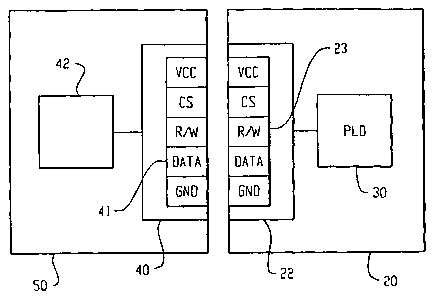
[0020] FIGURE 2 is a schematic diagram of an electrical connection between an
associated printer and the consumable of FIGURE 1;
[0021] FIGURE 3 is a schematic diagram showing an alternative programmable
device for use on a replaceable consumable;
[0022] FIGURE 4 is a further alternative embodiment of a configurable
processorfor
use on a replaceable consumable;
[0023] FIGURE 5 is a further embodiment of a configurable processor for use on
a
replaceable consumable;
[00241 FIGURE 6 is a flowchart illustrating a method of adapting a print
cartridge for
use with a printer in accordance with a preferred embodiment of the
application; and,
[0025] FIGURE 7 is a flowchart illustrating a method of adapting a print
cartridge
including an application specific integrated circuit for use with a printer in
accordance
with a further preferred embodiment of the application.
DETAILED DESCRIPTION OF THE PREFERRED EMBODIMENTS
[0026] Turning first to FIGURE 1, a replaceable consumable 10 is shown in
schematic form and illustrating the preferred embodiment of the present
application. As
illustrated, the consumable 10 includes a housing 12 defining a chamber
therein for
storing a marking material. In accordance with one aspect of the present
application,
the marking material is ink. In accordance with a further aspect, the marking
material is
toner. Other marking materials are also contemplated within the spirit and
scope of the
present application. Further, materials other than those used for marking can
be held in
the housing 12 as well such as, for example, chemicals used. in chemical
treatment or
process plants and other liquids, fluids, or flowing solids including edible
substances.
[0027] The housing 12 includes a front face wall 14 and a bottom outlet port
16
adapted to conduct a flow of the consumable marking material contained within
the
cartridge body therethrough. Those skilled in the art will appreciate that the
outlet port
16 includes o-rings, valves, or other mechanisms to provide a tight fluid
connection
between the associated printer (not shown) and the cartridge body to prevent
spillage
of the marking material.
CA 02635590 2008-06-26
WO 2007/079265 PCT/US2006/049674
[0028] The front face wall 14 of the housing 12, includes an electronic
circuit 20
carried thereon. The electronic circuit 20 includes communication circuit
portion 22 for
establishing a communication link between the circuit 20 and the associated
marking
device such as a printer or the like. The communication circuit portion 22 can
use any
known technologies such as electromechanical contact pads 23, infra red
transmitters
and receivers, and radio frequency devices.
[0029] As shown in FIGURE 2, the preferred form !of the subject electronic
circuit 20
includes a programmable logic device 30 connected with the communication
circuit
portion 20 for interfacing with a corresponding communication circuit 40
including a set
of electrical contacts 41 carried on the associated marking device 50. As
shown, the
marking device 50 includes a central processor 42. adapted to execute a
program
stored therein to interrogate the programmable logic device 30 of the
electronic circuit
20 carried on the consumable 10. To that end, the central processor 42 is in
operative
communication with the set of communication circuits 40 using an intermediary
electrical connection 44 to control voltage and logic levels on various
contact pad
portions of the set of electrical contacts 41. A chip select logic signal is
provided by a
CS contact pad. Read and write control is provided by the R/W contact pad.
Data is
provided at the DATA pad. Lastly, voltage is established for powering the
associated
electronic circuit 20 using a pair of voltage and ground pads, namely VCC and
GND.
[0030] The set of electrical contacts 23 carried on the electronic circuit 20
matches
those of the marking device 50. In accordance with the preferred embodiment,
the
programmable logic device 30 is in operative electrical communication with the
communication circuit portion 22 through an intermediary electrical connection
24.
Essentially, in its preferred form, the programmable logic device 30 responds
to signals
generated by the central processor 42 of the marking device 50 to provide the
necessary data and information for proper operation of the marking device 50.
[0031] Preferably, the subject programmable logic device includes an array of
AND
and OR gates which are programmable by fusing and/or diffusing selected
interconnections therebetween as understood by those skilled in the art. In
its preferred
form, the programmable logic device is a simple PLD arid, therefore, is
programmed via
a feasible link, antifuse, EPROM, EEPROM, or FLASH: - Alternatively, the
subject PLD
6
CA 02635590 2008-06-26
WO 2007/079265 PCT/US2006/049674
can be a complex PLD formed by a number of simple PLDs connected together by a
programmable switching matrix. In that embodiment, the complex PLD is a one of
an
EEPROM, FLASH, and SRAM based technology. -
[00321 FIGURE 3 shows an alternative embodiment of the electronic circuit
shown in
FIGURE 2. To that end, as illustrated in FIGURE 3, an electronic circuit 60
includes a
programmable logic device 30' in operative communication with a data storage
memory
62 and an input and output buffer circuit 64. The input/output buffer circuit
64 is
operatively connected with a communication circuit 66 adapted for operative
communication with a corresponding circuit 40 at the marking device 50. In the
embodiment illustrated in FIGURE 3, the programmable logic device includes an
array
of AND and OR gates which are programmable by fusing various links
therebetween.
The data memory 62 is used to store various information such as ink volume
which can
be updated by the marking device as necessary during operation thereof. An
input and
output circuit 64 is used to buffer the data and signals between the
electronic circuit 60
and the associated marking device 50.
[0033] FIGURE 4 is a schematic diagram of yet a further embodiment of an
electronic circuit 70 of the present application. As shown there, a
programmable logic
device 30" is in operative communication with a memory array 62' and an
application
specific integrated circuit core 72. In this embodiment, the ASIC core
provides all of the
fundamental operations of the circuit 70. However, additional functionality is
provided
by the programmable logic device 30" as may be deemed necessary during normal
evolution of the product life span of the consumable 10. In essence, the ASIC
functionality is augmented, modified, and improved during product life span by
reconfiguring the PLD portion 30" of the electronic circuit 70. A
communication circuit
76 is adapted for operative communication with a corresponding circuit 40
provided at
the marking device 50.
[0034] Turning lastly to FIGURE 5, a yet further alternative embodiment of an
electronic circuit 80 is shown in diagrammatical form. There, a field
programmable gate
array FGPA 82 is provided on the electronic circuit 80 in operative
communication with
a memory cell array 62". The memory cell array includes information relative
to the
marking material contained within the housing 12 such as, for example, ink
quantity,
7
CA 02635590 2008-06-26
WO 2007/079265 PCT/US2006/049674
type, color, and the like. The field programmable gate array includes a vast
array of
logical gates which are programmable via fusing in order to establish desired
function
behavior of the circuit relative to the marking device 50. A communication
circuit 86 is
included for operative communication with a corresponding circuit 40 at the
marking
device 50. 1
[0035] It is also understood and appreciated that the number of electrical
contacts
that are being used on the connection between the marking device and'the above
embodiments are not limited to five as shown in FIGURE 2 for example. It can
be any
number of contacts that are required to provide a proper and cost effective
interface
between the marking device and the electronic circuit.
[0036] It is also understood and appreciated that the interface between the
marking
device and the electronics circuit can also be Radio Frequency (RF) instead of
a direct
contacting interface.
[0037] FIGURE 6 shows a method 100 of adaptin.g a print cartridge for use with
a
printer in accordance with a further preferred embodiment of the present
app!ication.
With reference now to that figure, a processor is provided 102 on a first
print cartridge.
The processor is preferably a programmable logic device having configurable
internal
logic as described above. Thereafter, the processo'r is configured 104 so that
it is
operable with an associated printing device making the cartridge interoperable
with the
printing device. Preferably, the configuring at step 104 includes opening
fusible links
between logical AND and OR gates in the PLD device.
[0038] FIGURE 7 shows an alternative preferred embodiment of a method 110 for
adapting a print cartridge for use with a printer in accordance with the
application.
Initially, at step 112, a processor is provided connected with an application
specific
integrated circuit ASIC on a cartridge in a manner sub'stantially as described
above in
connection with FIGURE 4. Preferably, the processor has configurable logic and
includes a programmable logic device PLD. The PLD is connected together with
an
ASIC on a cartridge. Thereafter, at step 114, the logic within the processor
is
configured for adapting the ASIC and overall cartridge for use with the
associated
printing device. Preferably, the configuring includes opening fusible links
between
logical AND and OR gates in the programmable logic device.
8
CA 02635590 2008-06-26
WO 2007/079265 PCT/US2006/049674
[0039] it will be appreciated that various of the above-disclosed and other
features
and functions, or alternatives thereof, may be desirably combined into many
other
different systems or applications. Also that various presently unforeseen or
unanticipated alternatives, modifications, variations or improvements therein
may be
subsequently made by those skilled in the art which are also intended to be
encompassed by the following claims.
9