Note: Descriptions are shown in the official language in which they were submitted.
CA 02635774 2008-06-27
- 1 -
DESCRIPTION
LASER ANNEALING METHOD AND LASER ANNEALING DEVICE
Technical Field
[0001]
The present invention relates to a laser annealing
method and a laser annealing device that can reform an
amorphous semiconductor film into a polycrystalline
semiconductor film by applying a laser beam from a solid
laser source to the surface of the amorphous semiconductor
film.
Background Art
[0002]
In the field of semiconductor and liquid crystal, in
fabricating a thin film transistor (TFT), in order to
improve the mobility of carriers, a laser annealing
technique of forming polycrystalline silicon by applying a
laser beam to an amorphous silicon film (hereinafter,
referred to as "a-Si film") formed on a substrate to melt,
solidify, and re-crystallize the amorphous silicon film has
been performed.
In the laser annealing technique, a pulse laser beam
emitted from a laser source is processed into a rectangular
beam having a longitudinal section by the use of an optical
system and the rectangular beam is applied to the a-Si film
on the substrate while relatively moving the rectangular
CA 02635774 2008-06-27
- 2 -
beam relative to the applying surface in a short-side
direction of the beam.
[0003]
An excimer laser is conventionally used as the laser
source of the laser annealing technique, but a laser
annealing device using a laser beam obtained by converting
basic waves of a solid laser such as YAG, YLF, and YVO4
into a visible domain in wavelength has attracted attention
(for example, see Patent Documents 1 to 3). The solid
laser is useful because it is more advantageous in cost and
maintenance than the excimer laser.
In polycrystalline silicon devices or crystallized
silicon devices, it is reported that a wavelength-converted
beam of a solid laser can be used in processes of
activating impurities, etc.
[0004]
[Patent Document 11 Japanese Laid-Open Patent
Publication No. 2004-342954
[Patent Document 2] Japanese Laid-Open Patent
Publication No. 2004-63924
[Patent Document 3] Japanese Laid-Open Patent
Publication No. 2003-347237
[0005]
In a laser annealing device employing a visible beam
of a solid laser, crystals of a semiconductor film are made
to grow in the plane direction of the film (referred to as
"unidirectional growth") by uniformizing an energy
CA 02635774 2008-06-27
- 3 -
distribution in the long-side direction of the rectangular
laser beam but using the Gaussian energy distribution of
the original beam without processing the rectangular laser
beam in the short-side direction thereof, thereby obtaining
large-diameter crystal grains.
However, since an anisotropic property is given to
the crystal grains for the unidirectional growth and a
growing distance is affected by deviation in energy every
short of a laser pulse, it is difficult to fabricate
isotropic and uniform crystal grains. Accordingly,
characteristics of transistors are not uniform.
[0006]
Since the absorption coefficient of a visible beam
in a silicon film is low, the energy use efficiency of an
incident laser beam is low and much energy is required for
crystallization in the laser annealing technique using a
visible beam of the solid laser. Accordingly, there is a
problem that the processing ability is low.
By applying a laser beam with a low energy density
to slow the gradation of the Gaussian energy distribution
and thus to suppressing the unidirectional growing distance,
it is possible to obtain isotropic and uniform crystal
grains by the use of the solid laser. However, the
application of a laser beam with a low energy density
causes the more decrease in processing ability.
Disclosure of Invention
CA 02635774 2008-06-27
- 4 -
j0007]
The invention is contrived in consideration of the
above-mentioned problems. An object of the invention is to
provide a laser annealing method and a laser annealing
device that can provide isotropic and uniform crystal
grains and enhance the processing ability by using a solid
laser advantageous in cost and maintenance.
In order to achieve the above-mentioned object,
according to a first aspect of the invention, there is
provided a laser annealing method of reforming an amorphous
semiconductor film into a polycrystalline semiconductor
film by concentrating a laser beam emitted from a solid
laser source into a rectangular laser beam on the surface
of the amorphous semiconductor film and applying the
rectangular laser beam thereto while moving the rectangular
laser beam relative to the amorphous semiconductor film in
the short-side direction of the rectangular laser beam,
comprising the steps of: uniformizing an energy
distribution in the short-side direction of the rectangular
laser beam; and applying the rectangular laser beam to the
amorphous semiconductor film.
According to a second aspect of the invention, there
is provided laser annealing device for reforming an
amorphous semiconductor film into a polycrystalline
semiconductor film by concentrating a laser beam emitted
from a solid laser source into a rectangular laser beam on
the surface of the amorphous semiconductor film and
CA 02635774 2008-06-27
- 5 -
applying the rectangular laser beam thereto while moving
the rectangular laser beam relative to the amorphous
semiconductor film in the short-side direction of the
rectangular laser beam, comprising: a short-side-direction
uniformizing means for uniformizing an energy distribution
in a short-side direction of the rectangular laser beam,
short-side-direction uniformizing means being disposed in
an optical path of the laser beam.
The "rectangular beam" includes a visually linear
beam as a longitudinal rectangular beam.
[0008]
As the thermocoagulation analysis result of a
crystallization mechanism using a visible beam of a solid
laser, it can be seen that it is necessary to apply energy
(defined as "effective energy") greater than predetermined
energy so as to fabricate isotropic and uniform crystal
grains. It can be also seen that the diameter of the
crystal grains is determined by the number of input times
of the effective energy and the energy smaller than the
effective energy does not contribute to the growth of the
crystal grains. In the past, since the energy distribution
in the short-side direction of the rectangular beam applied
to the amorphous semiconductor film was the Gaussian
distribution, the effective energy range was a very small
range in the vicinity of the center of the Gaussian
distribution. Accordingly, when the transport speed of the
substrate is not made to be slow, the necessary number of
CA 02635774 2008-06-27
- 6 -
application times could not be obtained.
On the contrary, in the first and second aspects of
the invention, the energy distribution is converted from
the Gaussian distribution into a flat top shape by
uniformizing the energy distribution in the short-side
direction of the rectangular beam. In this way, by
converting the energy distribution, the effective energy
range can be widened with the same power as in the past.
Accordingly, the effective energy range in which the laser
beam is applied to the amorphous semiconductor film is
widened, thereby enhancing the transport speed of the
substrate as much. Therefore, it is possible to enhance
the processing ability of the laser annealing.
Since the energy distribution in the short-side
direction of the rectangular beam is uniformized, the
unidirectional growth of crystal grains cannot occur,
thereby fabricating the isotropic and uniform crystal
grains.
According to the first and second aspects, it is
possible to obtain the isotropic and uniform crystal grains
and to enhance the processing ability while using the solid
laser advantageous in cost and maintenance.
[0009]
A third aspect of the invention is an exemplary
embodiment of the second aspect, wherein the short-side-
direction uniformizing means includes a cylindrical lens
array or a light guide that dividing the laser beam into a
CA 02635774 2008-06-27
- 7 -
plurality of laser beams in the direction parallel to the
short-side direction of the rectangular laser beam and a
concentrating optical system that concentrates the beam
emitted from the cylindrical lens array or the light guide
on the surface of the amorphous semiconductor film in the
short-side direction of the rectangular laser beam.
A fourth aspect of the invention is an exemplary
embodiment of the second aspect, wherein the short-side-
direction uniformizing means is an optical system including
a diffracting optical element.
[0010]
According to the third and fourth aspects, since the
laser beam is divided in the direction parallel to the
short-side direction of the rectangular beam by the use of
the short-side-direction uniformizing means and the divided
laser beams are concentrated as a rectangular beam on the
surface of the amorphous semiconductor film, it is possible
to uniformize the energy distribution in the short-side
direction of the rectangular beam.
[0011]
A fifth aspect of the invention is an exemplary
embodiment of the second aspect, wherein the amorphous
semiconductor film is an amorphous silicon film.
[0012]
According to the fifth aspect, since the
polycrystalline silicon film having isotropic and uniform
crystal grains by annealing the amorphous silicon film, it
CA 02635774 2008-06-27
- 8 -
is possible to fabricate an excellent thin film transistor
(TFT) having high mobility of carriers.
[0013]
A sixth aspect of the invention is an exemplary
embodiment of the second aspect. In the laser annealing
device according to the invention, the solid laser source
may be one of an Nd:YAG laser, an Nd:YLF laser, an Nd:YVO4
laser, an Nd:glass laser, an Yb:YAG laser, an Yb:YLF laser,
an Yb: YVOq laser, and an Yb:glass laser.
[0014]
According to the sixth aspect, it is possible to
provide a high energy use efficiency of a stable laser beam
by using a solid laser with high reliability.
Brief Description of the Drawings
[0015]
Fig. 1 is a diagram illustrating an image of
effective energy in the conventional art and the invention.
Fig. 2 is a diagram illustrating dependence of an
average crystal grain size on the number of application
times of effective energy when a Gaussian rectangular beam
shown in Fig. 1 is applied.
Fig. 3 is a diagram illustrating dependence of the
number of application times of effective energy on a
substrate transport speed when a Gaussian rectangular beam
shown in Fig. 1 is applied.
Fig. 4 is a diagram schematically illustrating a
CA 02635774 2008-06-27
- 9 -
configuration of a laser annealing device according to a
first embodiment of the invention, where the configuration
is associated with the X direction (a long-side direction
of the rectangular beam).
Fig. 5 is a diagram schematically illustrating a
configuration of a laser annealing device according to a
first embodiment of the invention, where the configuration
is associated with the Y direction (a short-side direction
of the rectangular beam).
Fig. 6 is a diagram schematically illustrating a
configuration of a laser annealing device according to a
second embodiment of the invention, where the configuration
is associated with the X direction (a long-side direction
of the rectangular beam).
Fig. 7 is a diagram schematically illustrating a
configuration of a laser annealing device according to a
second embodiment of the invention, where the configuration
is associated with the Y direction (a short-side direction
of the rectangular beam).
Fig. 8 is a diagram illustrating an energy
distribution in the short-side direction when the energy
distribution in the short-side direction of the rectangular
beam is processed into a flat tope shape by the use of
short-side-direction uniformizing means 25 shown in Fig. 5.
Fig. 9 is a diagram illustrating a SEM image of a
sample to which the laser beam of which the energy
distribution in the short-side direction is processed into
CA 02635774 2008-06-27
- 10 -
a flat top shape is applied.
Fig. 10 is a diagram illustrating a relation between
an average grain size calculated from the SEM image shown
in Fig. 9 and an O.L ratio.
Fig. 11 is a diagram illustrating dependence of a
Raman half-value width on the O.L. ratio.
Best Mode for Carrying out the Invention
[0016]
Hereinafter, preferred embodiments of the invention
will be described in detail with reference to the
accompanying drawing. In the drawings, common elements are
denoted by like reference numerals and signs and repeated
description thereof is omitted.
[0017]
As described above, in a laser annealing process, a
pulse laser beam emitted from a laser source is
concentrated in a rectangular beam on the surface of a
amorphous semiconductor film (for example, an a-Si film)
formed on a substrate by the use of an optical system and
the rectangular beam is applied to the amorphous
semiconductor film while being moved relative to the
amorphous semiconductor film in the short-side direction of
the rectangular beam.
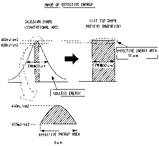
Fig. 1 is a diagram illustrating a shape (with peak
energy of 450 mJ/cm2 and a half-value width of 50 m) of an
energy distribution in the short-side direction on the
CA 02635774 2008-06-27
- 11 -
applying surface of the rectangular beam, where the left
side is a shape of the energy distribution in the
conventional art and the right side is a shape of the
energy distribution according to the invention. In the
past energy distribution in the short-side direction of the
rectangular beam has a Gaussian shape.
[0018]
As the thermocoagulation analysis result of the
crystallization mechanism using a visible beam of a solid
laser, the inventors found out that it is necessary to
apply energy (defined as "effective energy") greater than
predetermined energy so as to fabricate isotropic and
uniform crystal grains. When crystallizing the a-Si into
polycrystalline silicon, the effective energy is 430 mJ/cm2
or more. It could be seen that the diameter of the crystal
grains is determined by the number of application times of
the effective energy and the energy smaller than the
effective energy does not contribute to the growth of the
crystal grains.
In the past Gaussian energy distribution shown in
Fig. 1, the peak energy is 450 mJ/cm2, the half-value width
is 50 m, and the width of the effective energy region in
the short-side direction is 8 m.
[0019]
Fig. 2 shows the dependence of an average diameter
of the crystal grains on the number of application times of
the effective energy when the rectangular beam having the
CA 02635774 2008-06-27
- 12 -
Gaussian shape shown in Fig. 1 is applied. As shown in Fig.
2, the diameter of crystal grains is determined by the
number of application times of effective energy and the
energy smaller than the effective energy does not
contribute to the growth of the crystal grains as shown in
the left of Fig. 1.
Fig. 3 shows the dependence of the number of
application times of the effective energy on a substrate
transport speed when the rectangular beam having the
Gaussian shape shown in Fig. 1 is applied. In the past,
since the energy distribution in the short-side direction
of the rectangular beam has the Gaussian shape, the
effective energy range is a very small range (8 m in the
example shown in Fig. 1) in the vicinity of the center of
the Gaussian shape. Accordingly, when the substrate
transport speed is not made to be slow, the necessary
number of application times cannot be obtained.
[0020]
On the contrary, in the laser annealing method
according to the invention, the rectangular beam is
uniformized in energy distribution in the short-side
direction thereof and then is applied to the amorphous
semiconductor film.
The shape of the energy distribution in the short-
side direction of the rectangular beam applied in
accordance with the laser annealing method of the invention
is shown in the right side of Fig. 1. Since the energy
CA 02635774 2008-06-27
- 13 -
distribution in the short-side direction of the rectangular
beam is uniformized, the energy distribution is deformed
from the past Gaussian shape into a flat top shape.
As shown in Fig. 1, when the non-processed shape is
a Gaussian shape with the peak energy of 450 mJ/cm2 and the
half-value width of 50 m and the energy distribution of
the rectangular beam is processed into the flat top shape,
the effective energy region can be enlarged to 50 m with
the same input power.
[0021]
Accordingly, according to the laser annealing method
of the invention, the effective energy range is widened,
thereby enhancing the substrate transport speed as much.
In the above-mentioned example, by simple calculation, it
is possible to enhance the transport speed to 6.25 times so
as to obtain the crystal grains having the same diameter.
Therefore, it is possible to rapidly improve the processing
ability of the laser annealing process.
Since the energy distribution in the short-side
direction of the rectangular beam is uniformized, the
unidirectional growth of crystals does not occur, thereby
fabricating isotropic and uniform crystal grains.
Therefore, according to the invention, it is
possible to obtain the isotropic and uniform crystal grains
and to enhance the processing ability while using the solid
laser advantageous in cost and maintenance.
[0022]
CA 02635774 2008-06-27
- 14 -
A laser annealing device for embodying the laser
annealing method is described with reference to several
embodiments. However, the invention is not limited to the
below embodiments.
[0023]
First Embodiment
Figs. 4 and 5 are diagrams schematically
illustrating a configuration of a laser annealing device 10
according to a first embodiment of the invention. Fig. 4
is a configurational diagram corresponding to one direction
(defined as the X direction) perpendicular to the optical
axis of the solid laser source 12 and Fig. 5 is a
configurational diagram corresponding to the direction
(defined as the Y direction) perpendicular to the optical
axis of the solid laser source and the X direction. For
the purpose of easy understanding, optical elements acting
only in the Y direction are denoted by a virtual line in
Fig. 4 and optical elements acting only in the X direction
are denoted by a virtual line in Fig. 5.
[0024]
The laser annealing device 10 is a device for
reforming the amorphous semiconductor film into a
polycrystalline semiconductor film by concentrating the
laser beam 1 emitted from the solid laser source 12 in a
rectangular beam on the surface of the amorphous
semiconductor film formed on the substrate 3 and applying
the rectangular beam to the amorphous semiconductor film
CA 02635774 2008-06-27
- 15 -
while moving the rectangular beam relative to the amorphous
semiconductor film in the short-side direction thereof.
The relative movement is made by moving a substrate stage 5
having the substrate 3 mounted thereon in the short-side
direction (direction perpendicular to the paper surface of
Fig. 4) of the rectangular beam.
[0025]
In this embodiment, the substrate 3 is a glass
substrate. A Si02 film with a thickness of 200 nm is
formed on the substrate 3 by the use of a film forming
method such as a plasma CVD method and a sputtering method
and an a-Si film with a thickness of 50 nm is formed
thereon.
[0026]
In this embodiment, the laser annealing device 10
includes a solid laser source 12 emitting the laser beam 1,
a beam expander 14 enlarging the laser beam 1 from the
laser source 12 in the X direction and the Y direction, an
X-direction coherence reducing optical system 18 reducing
the coherence of the laser beam 1 in the X direction, an X-
direction cylindrical lens array 20 dividing the laser beam
1 into plural laser beams in the X direction, an X-
direction concentrating lens 22 concentrating the laser
beam 1, which has been divided into plural laser beams in
the X direction, on the applying surface, a Y-direction
coherence reducing optical system 24 reducing the coherence
of the laser beam 1 in the Y direction, a Y-direction
CA 02635774 2008-06-27
- 16 -
cylindrical lens array 26 dividing the laser beam 1 into
plural laser beams in the Y direction, and a Y-direction
concentrating lens 28 concentrating the laser beam 1, which
has been divided into plural laser beams in the Y direction,
on the applying surface,
[0027]
The solid laser source 12 outputs a pulse laser beam
1 at a pulse frequency of 2 to 4 kHz. The kind of the
solid laser source 12 is not particularly limited, but may
use one of an Nd:YAG laser, an Nd:YLF laser, an Nd:YVO4
laser, an Nd:glass laser, an Yb:YAG laser, an Yb:YLF laser,
an Yb: YVOq laser, and an Yb:glass laser. The solid lasers
can provide high reliability and can provide a high use
efficiency of stable laser energy.
Since the silicon film has a high absorption
coefficient in the visible domain of 330 nm to 800 nm, the
YAG laser, the YLF laser, the YVO9 laser, and the glass
laser emitting a second or third harmonic pulse laser beam
1 is suitable as the solid laser source 12.
[0028]
The beam expander 14 includes a concave spherical
lens 15 and a convex spherical lens 16 and serves to
enlarge the diameter of the laser beam 1 emitted from the
solid laser source 12 with the concave spherical lens 15
and to collimate the laser beam with the convex spherical
lens 16.
[0029]
CA 02635774 2008-06-27
- 17 -
Hereinafter, description is divided into the X
direction and Y direction. The X-direction processing of
the laser beam 1 is first described with reference to Fig.
4.
The X-direction coherence reducing optical system 18
includes plural transparent glass plates 18a. The width
(size in the X direction) of the respective transparent
glass plates is equal to the width (size in the X
direction) of the individual lenses of the X-direction
cylindrical lens array 20 and the transparent glass plates
18a having different lengths in the optical axis direction
by a predetermined length greater than the coherent length
of the laser beam 1 are arranged in the X direction. Since
the optical paths of the laser beam 1 having passed through
the transparent glass plates 18a is elongated by the length
of glass by the X-direction coherence reducing optical
system 18, the laser beam 1 has an optical path difference
greater than the coherent length and thus is not affected
by the coherence, thereby not cohering with each other.
[0030]
The laser beam 1 having been enlarged by the beam
expander 14 and having passed through the X-direction
coherence reducing optical system 18 is divided into plural
laser beams in the X direction by the X-direction
cylindrical lens array 20. The laser beams 1 divided while
passing through the X-direction cylindrical lens array 20
are focused once, are enlarged, and then is concentrated as
CA 02635774 2008-06-27
- 18 -
a rectangular beam longitudinal in the X direction on the
applying surface of the substrate 3 by the X-direction
concentrating lens 22 including a cylindrical lens. The
length in the long-side direction of the rectangular beam
can be set to, for example, several tens mm.
The rectangular beam is uniformized in energy
distribution in the long-side direction by passing through
the X-direction cylindrical lens array 20 and the X-
direction concentrating lens 22.
[0031]
The Y-direction processing of the laser beam 1 will
be described now with reference to Fig. S. The Y-direction
coherence reducing optical system 24 includes plural
transparent glass plates 24a. The width (size in the Y
direction) of the respective transparent glass plates 24a
is equal to the width (size in the Y direction) of the
individual lenses of the Y-direction cylindrical lens array
26 and the transparent glass plates 24a having different
lengths in the optical axis direction by a predetermined
length greater than the coherent length of the laser beam 1
are arranged in the Y direction. Since the optical path of
the laser beam 1 having passed through the respective
transparent glass plates 24a is elongated by the length of
glass by the Y-direction coherence reducing optical system
24, the laser beam 1 has an optical path difference greater
than the coherent length and thus is not affected by the
coherence, thereby not cohering with each other.
CA 02635774 2008-06-27
- 19 -
[0032]
The laser beam 1 having been enlarged by the beam
expander 14 and having passed through the Y-direction
coherence reducing optical system 24 is divided into plural
laser beams in the Y direction by the Y-direction
cylindrical lens array 26. The laser beams 1 divided while
passing through the Y-direction cylindrical lens array 26
are focused once, are enlarged again, and then are
concentrated as a rectangular beam having a small width in
the Y direction on the applying surface of the substrate 3
by the Y-direction concentrating lens 28 including two
cylindrical lenses 29 and 30. That is, the Y-direction
concentrating lens 28 corresponds to the "concentrating
optical system" of the claims.
[0033]
The concentrated rectangular beam is uniformized in
energy distribution in the short-side direction by passing
through the Y-direction cylindrical lens array 26 and the
Y-direction concentrating lens 28. That is, in this
embodiment, the Y-direction cylindrical lens array 26 and
the Y-direction concentrating lens 28 constitutes short-
side-direction uniformizing means 25 for uniformizing the
energy distribution in the short-side direction of the
rectangular beam. The length in the short-side direction
of the rectangular beam can be set to several tens m but
need to be set to have an energy density greater than the
effective energy density for the purpose of crystallization.
CA 02635774 2008-06-27
- 20 -
[0034]
As described above, the a-Si film is crystallized by
concentrating the laser beam 1 emitted from the solid laser
source 12 into a rectangular beam on the surface of the a-
Si film formed on the substrate 3 and applying the laser
beam 1 while transporting the substrate 3 in the short-side
direction of the rectangular beam by the use of a substrate
stage 5 at such a speed that the application ranges of the
laser pulse shots overlap with each other. At this time,
the transport speed of the substrate 3 is set so that the
number of overlapping application times of the laser pulse
shots is the number of application times of the effective
energy required for obtaining a predetermined crystal grain
size (for example, 250 to 350 nm).
[0035]
In this way, in the laser annealing device 10
according to the first embodiment, as shown in Fig. 1, the
energy distribution in the short-side direction of the
rectangular beam can be converted into a flat top shape by
uniformizing the energy distribution in the short-side
direction of the rectangular beam. Accordingly, the
effective energy range of the laser beam applied to the a-
Si film is widened and the transport speed of the substrate
3 can be enhanced, thereby improving the processing ability
of the laser annealing.
[0036]
In the first embodiment, the X-direction cylindrical
CA 02635774 2008-06-27
- 21 -
lens array 20 and the Y-direction cylindrical lens array 26
have different configurations, but they may be incorporated
into one lens array having both functions.
The X-direction coherence reducing optical system 18
and the Y-direction coherence reducing optical system 24
are not essential for the practice of the invention, but it
is possible to reduce the coherence of the solid laser beam
1 having high coherence and to apply the laser beam
uniformly, by using the coherence reducing optical systems.
The X-direction coherence reducing optical system 18 and
the Y-direction coherence reducing optical system 24 may
have other known configurations, and may employ the
configuration described in Japanese Laid-Open Patent
Publication No. 2002-321081 or the configuration shown in
Fig. 4 of Japanese Laid-Open Patent Publication No. 2004-
341299.
[0037J
Second Embodiment
Figs. 6 and 7 are diagrams schematically
illustrating a configuration of a laser annealing device 10
according to a second embodiment of the invention. Fig. 6
is a configurational diagram corresponding to the X
direction and Fig. 7 is a configurational diagram
corresponding to the Y direction.
For the purpose of easy understanding, optical
elements acting only in the Y direction are denoted by a
virtual line in Fig. 6 and optical elements acting only in
CA 02635774 2008-06-27
- 22 -
the X direction are denoted by a virtual line in Fig. 7.
The X and Y directions in Figs. 6 and 7 and the elements
denoted by the same reference numerals as in Figs. 4 and 5
represents the same meaning and configurations and thus
description thereof is properly omitted.
[0038]
The laser annealing device 10 is a device for
reforming the amorphous semiconductor film into a
polycrystalline semiconductor film by concentrating the
laser beam 1 emitted from the solid laser source 12 in a
rectangular beam on the surface of the amorphous
semiconductor film (an a-Si film in this embodiment) formed
on the substrate 3 and applying the rectangular beam to the
amorphous semiconductor film while moving the rectangular
beam relative to the amorphous semiconductor film in the
short-side direction thereof.
[0039}
In this embodiment, the laser annealing device 10
includes a solid laser source 12 emitting a laser beam 1, a
beam expander 14 enlarging the laser beam 1 from the laser
source 12 in the X and Y directions, an incidence lens 34
guiding the laser beam 1 to a light guide 36, a light guide
36 dividing the incident laser beam linto plural laser
beams in the X and Y directions, an X-direction end
transferring optical system 38 concentrating the laser
beams 1, which are divided in the X direction, in the X
direction and focusing the laser beams on the applying
CA 02635774 2008-06-27
- 23 -
surface so as to overlap with each other, an X-direction
coherence reducing optical system 42 reducing the coherence
in the X direction of the laser beams 1, a Y-direction end
transferring optical system 44 concentrating the laser
beams 1, which are divided in the Y direction, in the Y
direction and focusing the laser beams on the applying
surface so as to overlap with each other, and a Y-direction
coherence reducing optical system 48 reducing the coherence
in the Y direction of the laser beams 1.
[0040]
The light guide 36 is an optical element which is
formed of a transparent member having a solid parallel
hexahedral shape and which includes X-direction reflecting
surfaces 36a and 36b facing each other with a distance
therebetween in the X direction along the optical axis and
Y-direction reflecting surfaces 36c and 36d facing each
other with a distance therebetween in the Y direction along
the optical axis, and is made of, for example, BK7 or light
refracting glass. The number of channels of the laser
beams 1 in the X direction and the Y direction can be set
on the basis of the distance between the X-direction
reflecting surfaces 36a and 36b, the distance between the
Y-direction reflecting surfaces 36c and 36d, and the length
in the optical axis direction of the light guide 36.
[0041]
Hereinafter, description is divided into the X
direction and Y direction. The X-direction processing of
CA 02635774 2008-06-27
- 24 -
the laser beam 1 is first described with reference to Fig.
6.
The laser beam 1 enlarged by the beam expander 14 is
guided to the light guide 36 by the incidence lens 34 and
is divided into plural laser beams in the X direction. The
laser beams 1 divided by the light guide 36 are transferred
in the X direction by the X-direction end transferring
optical system 38 including two cylindrical lenses 39 and
40 and are focused on the applying surface of the substrate
3 as a rectangular beam longitudinal in the X direction.
The length in the long-side direction of the rectangular
beam can be set to, for example, several tens mm. The X-
direction coherence reducing optical system 42 is disposed
between two cylindrical lenses 39 and 40 of the X-direction
end transferring optical system 38 to reduce the coherence
by giving an optical path difference to the divided laser
beams 1.
The rectangular beam is uniformized in energy
distribution in the long-side direction by passing through
the light guide 36 and the X-direction end transferring
optical system 38.
[0042]
The Y-direction processing of the laser beam 1 is
described now with reference to Fig. 7.
The laser beam 1 enlarged by the beam expander 14 is
guided to the light guide 36 by the incidence lens 34 and
is divided into plural laser beams in the Y direction. The
CA 02635774 2008-06-27
- 25 -
laser beams 1 divided by the light guide 36 are transferred
in the Y direction by the Y-direction end transferring
optical system 44 including two cylindrical lenses 45 and
46 and are focused on the applying surface of the substrate
3 as a rectangular beam narrow in the Y direction. The Y-
direction coherence reducing optical system 48 is disposed
between two cylindrical lenses 45 and 46 of the Y-direction
end transferring optical system 44 to reduce the coherence
by giving an optical path difference to the divided laser
beams 1. The Y-direction end transferring optical system
44 corresponds to the "concentrating optical system" of the
claims.
[0043]
The concentrated rectangular beam is uniformized in
energy distribution in the short-side direction by passing
through the light guide 36 and the Y-direction end
transferring optical system 44. That is, in this
embodiment, the light guide 36 and the Y-direction end
transferring optical system 44 constitutes short-side-
direction uniformizing means 25 for uniformizing the energy
distribution in the short-side direction of the rectangular
beam. The length in the short-side direction of the
rectangular beam can be set to several tens m but need to
be set to have an energy density greater than the effective
energy density for the purpose of crystallization.
[0044]
As described above, the a-Si film is crystallized by
CA 02635774 2008-06-27
- 26 -
concentrating the laser beam 1 emitted from the solid laser
source 12 into a rectangular beam on the surface of the a-
Si film formed on the substrate 3 and applying the laser
beam 1 while transporting the substrate 3 in the short-side
direction of the rectangular beam by the use of a substrate
stage 5 at such a speed that the application ranges of the
laser pulse shots overlap with each other. At this time,
the transport speed of the substrate 3 is set so that the
number of overlapping application times of the laser pulse
shots is the number of application times of the effective
energy required for obtaining a predetermined crystal grain
size (for example, 250 to 350 nm).
[0045]
In this way, as shown in Fig. 1, the energy
distribution in the short-side direction of the rectangular
beam can be converted into a flat top shape by uniformizing
the energy distribution in the short-side direction of the
rectangular beam. Accordingly, the effective energy range
of the laser beam applied to the a-Si film is widened and
the transport speed of the substrate 3 can be enhanced,
thereby improving the processing ability of the laser
annealing.
[0046]
In the second embodiment, the laser beam 1 is
divided in the X direction and the Y direction by the use
of the same light guide 36, but a light guide for division
in the X direction and a light guide for division in the Y
CA 02635774 2008-06-27
- 27 -
direction may be separately provided.
The short-side-direction uniformizing means is not
limited to the description in the first and second
embodiments, but the energy distribution in the short-side
direction of the rectangular beam may be uniformized by the
use of the well-known optical systems. For example, the
short-side-direction uniformizing means may be an optical
system including a diffracting optical element. The
detailed description of the diffracting optical element is
omitted, which is disclosed, for example, in Japanese Laid-
Open Patent Publication No. 2005-217209. In the
diffracting optical element, minute steps are formed on a
substrate of quartz or the like by photolithography and
etching processes and diffraction patterns formed by the
laser beam passing through the steps are fabricated so as
to obtain a desired energy distribution on a focusing
surface (substrate surface).
[0047]
Examples
Hereinafter, examples of the invention will be
described.
Fig. 8 is a diagram illustrating the short-side
energy distribution when the energy distribution in the
short-side direction of the rectangular beam is processed
into a flat top shape by the short-side-direction
uniformizing means 25 shown in Fig. 5. It can be seen from
Fig. 8 that both ends droop due to the insufficient
CA 02635774 2008-06-27
- 28 -
optimization but the flat region of 75 m is secured.
[0048]
Fig. 9 shows a SEM (Scanning Electron Microscope)
image of an a-Si film to which a laser beam of which the
short-side energy distribution has been processed into a
flat top shape is applied. Fig. 10 shows a relation
between an average grain size calculated from the SEM image
shown in Fig. 9 and an O.L. (overlap) ratio of two kinds of
the flat tope shape and the Gaussian shape. The O.L. ratio
means a ratio of a distance, which the substrate moves
every laser shot by, to the flat region (half-value width
in the Gaussian shape).
It can be seen from Fig. 10 that the Gaussian shape
provide an average grain size of 300 to 400 nm at the O.L.
ratio of 97% to 98%, while the flat top shape provides an
average grain size of 400 nm or more even at the O.L. ratio
of 91%. When it is converted into the transport speed, it
can be seen that the transport speed increases 4.4 times in
maximum.
[0049]
Fig. 11 shows dependence of a Raman half-value width
on the O.L. ratio. The Raman half-value width is an
indicator indicating a crystallization property and
indicates that the performance is more excellent it gets
close to the half-value width (4 cm-1) of the crystalline
silicon. As can be clearly seen form this result, a more
excellent crystalline state can be obtained from the flat
CA 02635774 2008-06-27
- 29 -
top shape than the Gaussian shape.
[0050]
As can be clearly seen from the above description,
according to the invention, it is possible to obtain
isotropic and uniform crystal grains and to enhance the
processing ability by using a solid laser advantageous in
cost and maintenance.
[0051]
Although the embodiments of the invention have been
described, the embodiments are merely exemplary and the
invention is not limited to the embodiments. For example,
although it has been described in the above-mentioned
embodiments that the a-Si film is used as the amorphous
semiconductor film, other amorphous semiconductor films
(for example, a compound semiconductor film such as an
amorphous silicon germanium film having an amorphous
structure) may be used.
The scope of the invention is determined by the
appended claims and includes all the modifications and
changes equivalent to the claims and within the scope of
the claims.