Note: Descriptions are shown in the official language in which they were submitted.
CA 02637788 2008-07-18
WO 2007/083178
PCT/1B2006/003207
- 1 -
"METHOD AND DEVICE FOR MEASURING THE THICKNESS OF A LAYER OF
MATERIAL"
TECHNICAL FIELD
The present invention relates to a method and a device for
measuring the thickness of a layer of material.
In particular, the present invention finds advantageous, but
non-exclusive, application in the measurement of the thickness
of a layer of a paper pulp in a draining station of a
papermaking machine, to which the ensuing description will
make explicit reference, without this, however, implying any
loss of generality.
BACKGROUND ART
As is known, in a papermaking machine, a layer of paper pulp,
in which the part of water is approximately 98%, is fed along
a path for production of the paper, which traverses, in
succession, a station for draining the layer of paper pulp, a
station for pressing the layer of paper pulp, and a station
for drying the layer of paper pulp.
A first portion of the production path that traverses the
draining station defines, a draining path, along which the
layer of paper pulp advances laid on a fabric that rotates in
a loop. Set underneath the fabric are, at a regular distance
from one another, a plurality of suction units for aspirating
the water, through the fabric, from the paper pulp as it
advances.
A high efficiency of the draining station reduces the cost of
the treatment carried out by the drying station downstream.
For the above purpose, existing on the market are devices for
controlling the thickness of water in the paper pulp, which
comprise a rod, mounted on which is a read head provided with
CA 02637788 2015-04-16
=
- 2 -
a sensor for measurement of the amount of water. These devices
are usually positioned manually in such a way that the sensor
is brought into contact with the bottom surface of the fabric
between one suction unit and another.
Said devices use various types of sensors, for example sensors
that exploit GBS (Gamma Back Scattering) technology for
detecting the consistency of the material with which they come
into contact. Said technology is accurate but requires the
presence of a radioactive source inside the read head and is
consequently costly and impractical. Other sensors exploit
ultrasound and are hence less costly than the previous ones,
but also more difficult to use in noisy environments, such as
those of papermaking machines. Yet other sensors exploit
microwaves, and in particular estimate the consistency of. the
material from the frequency response of the material itself,
but are cumbersome and do not yield sufficiently reliable
measures.
DISCLOSURE OF THE INVENTION
The aim of the present invention is to provide a method and a
device for measuring the thickness of a layer of material, and
in particular the thickness of water of a layer of paper pulp
and water for the production of paper, that will be free from
the drawbacks described above and at the same time will be
easy and inexpensive to produce.
=
In accordance with the present invention, a method and a
device are provided for measuring the thickness of a layer of
material according to what is defined in the attached
independent claims and, preferably, in any one of the claims
that depend either directly or indirectly upon the
aforementioned independent claims.
ak 02637788 2015-04-16
- 2a -
In one form of this disclosure, there is provided a method
for measuring the thickness of a layer of first material,
the method comprising the step of
- acquiring at least one frequency response of the layer of
first material via a microwave sensor;
- setting the microwave sensor on a plurality of specimens
of second materials for different temperature values (Tamb,
Ti, T2, T3) in such a way as to obtain reference data (CD,
X, Y, S);
- calibrating the microwave sensor as a function of the
electrical conductivity of the first material using the
reference data (CD, X, Y, S);
- measuring the temperature (Tm) of the layer of first
material via a temperature sensor;
- determining measurement parameters (Fl_m, F2_m, Amin_m)
of the layer of first material from the frequency response;
and
- processing the reference data (CD, X, Y, S) with the
measurement parameters (Fl_m, F2_m, Amin_m) and the measured
temperature (Tm) to obtain a measurement (Sm) of the
thickness of the layer of first material; the method being
characterized in that the step of calibrating the microwave
sensor comprises the step of determining a calibration
parameter (INTc) as a function of the electrical
conductivity of the first material and of first ones (CD, X,
Y) of said reference data.
BRIEF DESCRIPTION OF THE DRAWINGS
For a better understanding of the present invention, a
CA 02637788 2008-07-18
WO 2007/083178
PCT/1B2006/003207
- 3 -
preferred embodiment thereof is now described, purely by way
of non-limiting example and with reference to the attached
plate of drawings, wherein:
- Figure 1A and Figure 1B illustrate a preferred embodiment of
the device for measuring the thickness of a layer of material
according to the present invention;
- Figure 2 illustrates a block diagram of a control unit of
the device of Figure 1;
- Figures 3 to 8 illustrate, as a whole, a flowchart of the
method for measuring the thickness of a layer of material
according to the present invention;
- Figures 9 to 14 illustrate examples of frequency-response
curves of specimens of materials and of corresponding setting
and calibration curves of the device of Figure 1, obtained and
used following the method for measuring the thickness of a
layer of material according to the present invention; and
- Figures 15 and 16 illustrate examples of frequency responses
of the layer of material acquired and processed following the
method for measuring the thickness of a layer of material
according to the present invention.
BEST MODE FOR CARRYING OUT THE INVENTION
In Figure 1A, the reference number 1 designates, as a whole,
the device for controlling the thickness of a material, said
device 1 comprising: a control unit 2; a read head 3, designed
to be set in contact with a layer of material (not
illustrated) and in particular a layer of paper pulp and water
in order to measure the thickness thereof; and a supporting
rod 4, having a first end 5, in a position corresponding to
which the read head 3 is mounted, and a second end 6, mounted
on which is a connector 7 provided with an electrical cable 8
for connection of the read head 3 to the control unit 2.
The control unit 2 comprises a front control panel 9 provided
with a display 10, for example of the backlighted liquid-
crystal type with a resolution of 128x128 pixels, for
CA 02637788 2013-10-18
- 4 -
displaying information on the measurements, and a keypad 11, via
which an operator can impart commands on the control unit 2. The
control unit 2 further comprises a plurality of connectors 12 for
connection to the read head 3 and with further external control
devices (not illustrated), for example a personal computer.
The read head 3 comprises a microwave sensor 13 and a temperature
sensor 14. In particular, the microwave sensor 13 is, for example,
of the type described in the Italian patent Publication No.
ITMI20060084, in the name of ADVANCED MICROWAVE ENGINEERING, and
comprises a microwave transmitter and a respective microwave
receiver for detecting, through the material, the signals
generated by the transmitter. In particular, the sensor 13 is
characterized by a frequency-response curve substantially centered
around a resonance frequency, for which there is a minimum value
of amplitude. The presence of the material in the neighbourhood of
the sensor 13 modifies the response curve, in terms of shift of
the resonance frequency and of variation of the minimum amplitude,
in a way that depends upon the physical characteristics of the
material itself.
The supporting rod 4 is provided with a signalling element 15, for
example of an optical type or else of an acoustic type, for
signalling that the measurement is in progress, and with a small
level 16 for verifying proper positioning of the supporting rod 4
and, hence, of the read head 3. In greater detail, as illustrated
in Figure 1B, the supporting rod 4 comprises a telescopic arm 17,
which is extensible at its first end 5 and mounted on which is the
read head 3.
With reference to Figure 2, the control unit 2 comprises, in
addition to the aforementioned display 10 and keypad 11, a storage
unit 18, for example a removable flash memory of the type referred
to as "smart media card", designed to store the
CA 02637788 2008-07-18
WO 2007/083178
PCT/1B2006/003207
-
data on the measurements, an interface unit 19, for
communication with the external control devices, an interface
unit 20 for communication with the sensors 13, 14, a
processing unit 21, for example of the type comprising a
5 microcontroller, connected for communication with the display
10, with the keypad 11, and with all the other units mentioned
above, and a supply unit 22, which is designed to supply
electrically all the units mentioned above.
In greater detail, the display 10 is designed to display the
state of the sensors 13, 14, the data regarding the
measurement in progress, and the statistics regarding the
previous measurements. Amongst the commands that can be
imparted via the keypad 11 there is, for example, the number
of measurement samples to be acquired via the device 1.
The supply unit 22 comprises a battery (not illustrated),
preferably of the rechargeable type, and a supervision and
signalling circuit (not illustrated either), for monitoring
the residual level of charge of the battery, to said level
there being associated an appropriate indicator represented,
for example, via a warning light or via an icon displayed on
the display 10.
Each of the interface units 19, 20 is constituted, for
example, by a serial port of the RS232 or USB type.
Figures 3 to 7 show respective portions of a flowchart of the
method for measuring the thickness of a layer of a material
according to the present, invention, said method being
implemented in a control program (firmware) loaded into the
microcontroller of the processing unit 21.
The principle underlying the method for measuring the
thickness of a layer of a material consists in: obtaining
reference data from a setting of the microwave sensor 13
CA 02637788 2008-07-18
WO 2007/083178
PCT/1B2006/003207
- 6 -
carried out in laboratory on specimens of known materials in
known physical conditions; calibrating the sensor 13 on the
basis of the electrical conductivity of the material under
examination, i.e., of the material of the layer to be
measured, using, for example, a specimen of said material; and
determining a measurement of the thickness from a frequency
response of the layer of material, acquired by means of the
sensor 13, and as a function of the temperature Tm of the
layer of material measured with the sensor 14.
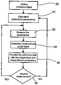
With reference to Figure 3, the method for measuring the
thickness of a layer of material envisages a step of setting
of the sensor 13 (block 30) on specimens of materials that
have respective given values of electrical conductivity for -
temperature values determined in such a way as to obtain the
reference data; a step of calibration of the sensor 13 (block
31) as a function of the electrical conductivity of the
material under examination, i.e., of the material of the layer
to be measured using the reference data for determining
calibration parameters; a step of measurement of the
temperature Tm of the layer of material under examination
(block 32); a step of determination of measurement parameters
of the layer of material from a frequency response of the
layer itself using the calibration parameters (block 33); and
a step of processing of the reference data with the
measurement parameters and the temperature Tm for determining
a measurement Sm of the thickness of the layer itself (block
34).
The steps indicated with blocks 32, 33 and 34 are repeated,
whenever required, to obtain a measurement of the thickness;
otherwise, control returns to the calibration step (block 35).
The step of setting of the sensor 13 (block 30 of Figure 3) is
carried out once and for all in the laboratory and is
illustrated, in all its substeps, in Figure 4 and described
CA 02637788 2008-07-18
WO 2007/083178
PCT/1B2006/003207
- 7 -
hereinafter.
The step of setting of the sensor 13 envisages, in the first
place, obtaining reference data constituted by data of
thickness S of a material determined as the working frequency
F of the sensor 13 varies in a frequency band FB, comprised
between a minimum value Fmin and a maximum value Fmax, and for
given temperature values Ti, T2, T3.
Said data of thickness S as a function of the frequency F are
obtained by: acquiring, via the sensor 13, for each value of
temperature Ti, T2, T3, a plurality of frequency-response
curves of a respective plurality of specimens of a material
having a value CD1 of electrical conductivity, each specimen
having a respective value of substance or thickness S (block
40); and associating to each value of thickness S a respective
value of frequency F identified by the intersection of the
response curve corresponding to said value of thickness S with
a function that is constant in frequency, referred to
hereinafter, for reasons of convenience, as "intercept
straight line" (block 41).
Figure 9 is a graphic illustration of an example of how to
obtain the data of thickness S as the frequency F varies for
any of the temperature values Ti, T2, T3.
The graph in the top part in Figure 9 illustrates the
frequency-response curves, which are constituted by as many
patterns of amplitude A of the output signal of the sensor 13
as the frequency F varies in the band FB for the different
values of the thickness S. The amplitude A is dimensionless in
so far as the output of the sensor 13 corresponds to the
output of an A/D converter of the sensor 13. The intercept
straight line assumes a first value INT1 substantially equal
to half of the output range of the AID converter, and in
particular equal to 2500. Each value of frequency F associated
CA 02637788 2008-07-18
WO 2007/083178
PCT/1B2006/003207
=
- 8 -
-
to the respective value of thickness S is defined by the
intersection of the intercept straight line of value INT1 with
the increasing stretch of the frequency-response curve
corresponding to the value of thickness S itself.
The graph at the bottom of Figure 9 represents an example of
pattern of the thickness S as a function of the frequency F
obtained associating the values of frequency F obtained to the
values of thickness S.
Figure 10 illustrates examples of curves of the thickness S as
a function of the frequency F for the different temperature
values Tl, T2 and T3 that increase so that T3>T2>T1, and
preferably are equal to 10 C, 35 C, and 60 C, respectively.
The data of thickness S as a function of the frequency F for
the three temperature values Ti, T2 and T3 are gathered in a
corresponding look-up table stored in the storage unit 18.
The step of setting of the sensor 13 moreover envisages
obtaining other reference data, constituted by data of
electrical conductivity CD as a function of the minimum
amplitude Amin of the output signal of the sensor 13 at a
constant ambient temperature of value Tamb.
Once again with reference to Figure 4, the data of
conductivity CD as a function of the minimum amplitude Amin
are obtained by: acquiring, via the sensor 13, a plurality of
frequency-response curves, in the frequency band FE, of a
respective plurality of specimens of materials that each have
a respective value of electrical conductivity CD (block 42);
and associating, to each value of electrical conductivity CD,
the value of minimum amplitude Amin of the frequency-response
curves of the specimen that has said value of electrical
conductivity CD (block 43).
CA 02637788 2008-07-18
WO 2007/083178
PCT/1B2006/003207
- 9 -
Figure 11 illustrates examples of frequency-response curves of
materials having different values of the electrical
conductivity CD and highlights the values of minimum amplitude
Amin of each curve designated by Ao, Al, A2, A3f A4 and A5. Said
minima occur at the resonance frequency of the corresponding
material. Figure 12 shows an example of pattern of the
electrical conductivity CD as a function of the minimum
amplitude Amin obtained from the data derived from Figure 11.
The data of electrical conductivity CD as a function of the
minimum amplitude Amin at ambient temperature Tamb are
gathered in a corresponding look-up table stored in the
storage unit 18.
Finally, the step of setting of the sensor 13 envisages
determining a linear function between the generic value INT of
intercept straight line and the electrical conductivity CD of
the material under examination at constant temperature, and in
particular at the value of temperature T2. In other words, the
step of setting envisages determining further reference data
constituted by the coefficients X and Y that identify a linear
function of the type INT = X * CD + Y.
In particular, once again with reference to Figure 4, the step
of setting of the sensor 13 envisages acquiring, via the
sensor 13 itself, three sets of frequency-response curves for
three different values of reference thickness SR, SR', SR" of
material, in which each group of curves comprises three
frequency-response curves of three materials having respective
values of electrical conductivity CD1, CD2, CD3 (block 44).
The values of electrical conductivity CD1, CD2 and CD3 are
increasing so that CD3>CD2>CD1, and preferably equal to 1500,
4000, and 6500 S/cm, respectively. The values of reference
thickness SR, SR' and SR" are decreasing and preferably equal
to 25000, 10000, and 5000 g/m2, respectively.
CA 02637788 2008-07-18
WO 2007/083178
PCT/1B2006/003207
- 10 -
For each of said groups of frequency-response curves, the
following data are determined: a respective value of frequency
Fl, F1', Fl" from the intersection of the curve corresponding
to the material with electrical conductivity CD1 with the
intercept straight line of a first value INT1 (block 45); a
second value INT2, INT2', INT2", and a third value INT3,
INT3', INT3" that the intercept straight line must assume for
identifying the same value of frequency Fl, F1', Fl" in the
presence of the material with electrical conductivity having
value CD2 and, respectively, CD3 given the same reference
thickness SR, SR' and SR" (block 46).
At this point, the values INT1, INT2, INT2', INT2", INT3,
INT3', and INT3", corresponding to the different values of
reference thickness SR, SR' and SR" are averaged with one
another in such a way as to obtain a mean value INT1, INT2m,
INT3m of intercept straight line for each value of electrical
conductivity CD1, CD2, CD3 (block 47). The coefficients X and
Y are determined according to the series of values of
electrical conductivity CD1, CD2, CD3 and of the respective
series of mean values INT1, INT2m, INT3m using any known
linear-regression technique (block 48).
Figure 13 illustrates an example of determination of the
values INT2, INT2', INT2", INT3, INT3' and INT3".
Figure 14 illustrates an example of linear relation between
the value INT of intercept straight line and the electrical
conductivity CD obtained by linear regression. Also the
coefficients X and Y are stored in the storage unit 18.
The step of calibration of the sensor 13 (block 31 of Figure
3) has the purpose of determining a calibration parameter
constituted by a value INTc of the intercept straight line in
the presence of a specimen of the material under examination
CA 02637788 2008-07-18
WO 2007/083178
PCT/1B2006/003207
- 11 -
at the constant ambient temperature of value Tamb.
The calibration is carried out previously by immersing the
read head 3 in a purposely provided calibration cup containing
a specimen of the material under examination. Alternatively,
the calibration is carried out automatically by the device 1
during the normal operations of measurement of the thickness
of the layer of material.
In general, the step of calibration envisages: acquiring
frequency-response curves of the material under examination in
the frequency band FB similar to the ones illustrated in
Figures 9 and 10; finding a value of minimum amplitude Amin_c
of said curves; and processing said value of minimum amplitude
Amin c to obtain the value INTc of the intercept straight
line.
In particular, with reference to Figure 5, acquisition of the
frequency-response curves occurs by: incrementing the
frequency F from the minimum value Fmin (block 50) to the
maximum value Fmax (block 51) according to a given frequency
step Fs in particular of a value of 10 kHz (block 52); and
acquiring a value of amplitude A of the signal at output from
the sensor 13 for each value of frequency F set (block 53).
The value of minimum amplitude Amin_c of the curve is found
by: initially setting the minimum amplitude Amin_c at a
sufficiently high value, and in particular at a maximum value
Alim of the dynamic output range of the sensor 13 equal to
4095 (block 50); comparing, for each value of frequency F set,
the minimum amplitude Amin_c set with each value of amplitude
A acquired (block 54); and replacing the minimum amplitude
Amin c set with the value of amplitude A in the case where the
latter is lower (block 55).
Once the value of minimum amplitude Amin_c is identified, it
CA 02637788 2008-07-18
WO 2007/083178
PCT/1B2006/003207
- 12 -
is compensated according to the relation:
Amin c = (Tmc - Tamb)*KC + Amin c,
where Tmc corresponds to the temperature of the material
during the step of measurement proper and can be set by the
operator via the keypad 11 during the present step of
calibration, and KC is a coefficient that depends upon the
mechanical and electronic characteristics of the read head 3
and is purposely determined in the laboratory in an empirical
way (block 56).
Next, a measurement of the electrical conductivity CDc of the
material under examination is determined, by extracting it, by
means of interpolation, from the data of electrical
conductivity CD using the value of minimum amplitude Amin_c
(block 57), and a value INTc of intercept straight line is
determined as a function of the value of electrical
conductivity CDc using the coefficients X and Y, i.e., using
the linear function of the type illustrated in Figure 14
(block 58).
At this point, once the steps of setting and calibration of
the sensor 13 have been completed, the operations that lead to
the determination of a measurement of the thickness are
carried out.
The measurement of the temperature Tm of the material under
examination (block 32 of Figure 3) is followed, as has already
been mentioned previously, by the step of determination of
measurement parameters (block 33 of Figure 3). Said
measurement parameters comprise a value of intercept frequency
Fl m determined for a range of values of amplitude A of a
frequency response of the layer of material acquired via the
sensor 13, said range being substantially centred around the
value INTc of the intercept straight line obtained during the
CA 02637788 2008-07-18
WO 2007/083178
PCT/1B2006/003207
- 13 -
calibration of the sensor 13.
More precisely, with reference to Figure 6, the determination
of the mean value Fl m of frequency comprises the steps of:
- initially setting the working frequency F of the sensor 13
to the maximum value Fmax, the frequency step Fs to a maximum
or coarse value Fs_g, in particular equal to 1 MHz, a
tolerance T of the amplitude A to the highest value that can
be selected, i.e., to the maximum or coarse value T_g, a
counter of calculation iterations C to a determined value N of
iterations, the intercept straight line to the value INTc of
intercept straight line determined previously with the
calibration of the sensor 13, and the intercept frequency Fl_m
to a starting zero value (block 60);
- comparing the current value of the frequency F with the
maximum value Fmax and the minimum value Fmin (block 62) to
enable warning of possible out-of-range settings of the
frequency F (block 63) and consequently resetting the
parameters set in the previous step represented by block 60
(block 64);
- acquiring a value of amplitude A of the signal at output
from the sensor 13 (block 65); and
- comparing the value of amplitude A acquired with the value
INTc of intercept straight line (block 66) and comparing the
difference, in absolute value, between the value of amplitude
A and the value INTc with the value of tolerance T set (blocks
67 and 68) in order to distinguish the cases described
hereinafter.
If both of the conditions below are satisfied:
A < INTc; and
IA - INTc1 < T,
then the frequency step Fs is set to a minimum or fine value
Fs _f (Fs = Fs f), and the tolerance T to a minimum or accurate
CA 02637788 2008-07-18
WO 2007/083178
PCT/1B2006/003207
- 14 -
value T f (T = T f), and the frequency F is incremented by the
frequency step Fs (F = F + Fs) (block 69), and the flow
proceeds with the subsequent block 71. The minimum value of
tolerance T f is, for example, equal to 1% of the value of
INTc of the intercept straight line.
If both of the conditions below are satisfied:
A < INTc; and
IA - INTcl T,
then the frequency step Fs is set to the maximum value Fs_g
(Fs = Fs_g), and the tolerance T to its maximum value T_g (T =
T_g), the frequency F is incremented by the frequency step Fs
(F = F + Fs) (block 74), and control returns to block 62.
If both of the conditions below are satisfied:
A INTc; and
IA - INTcl < T,
then the frequency step Fs is set to the minimum value Fs_f
(Fs = Fs f), the tolerance T is set to the minimum value T f
(T = T_f), the frequency F is decremented by the frequency
step Fs (F = F - Fs) (block 70), and the flow proceeds with
the subsequent block 71.
If both of the conditions below are satisfied:
A INTc; and
IA - INTcl T,
then the frequency step Fs is set to the maximum value Fs_g
(Fs = Fs_g), and the tolerance T to the maximum value T_g (T =
T_g), the frequency F is decremented by the frequency step Fs
(F = F - Fs) (block 75), and control returns to block 62.
CA 02637788 2008-07-18
WO 2007/083178
PCT/1B2006/003207
- 15 -
,
Following upon increment or decrement of the frequency F by
the frequency step Fs from or to the minimum value Fs_f
(output of block 69 or block 70), the following steps are
envisaged:
- accumulating the current frequency value F adding it to the
intercept frequency Fl_m (Fin = Fl_m + F) and decrementing by
one the counter of iterations of calculation C (C = C - 1)
(block 71);
- verifying the residual number of iterations of calculation
(block 72): if said number is zero (C = 0), then the flow
proceeds with the next block 73; otherwise control returns to
block 62; and
- calculating the value of intercept frequency Fl_m sought as
mean value of the values accumulated (block 73).
Figure 15 illustrates an example of determination of the value
of intercept frequency Fl_m. As may noted, the frequency
response is acquired by decrementing the working frequency F
of the sensor 13 starting from the maximum value Fmax up to ,
values of frequency corresponding to values of amplitude A
comprised in a range DT centred around the value INTc and of
extension equal to twice the minimum value T_f of the
tolerance T. In other words, the frequency response acquired
is constituted by a range of values of amplitude A, which
increase as the frequency F increases and are distributed
around the value INTc.
Processing of the reference data with the measurement
parameters and the temperature of the layer of material under
examination for determining a measurement of the thickness of
the layer itself (block 34 in Figure 3) initially envisages
extracting three first-approximation values of thickness Si,
S2, 53 from the data of thickness S as a function of the
frequency F for the three different temperatures Ti, T2 and T3
using the intercept frequency Fl_m.
CA 02637788 2008-07-18
WO 2007/083178
PCT/1B2006/003207
- 16 -
In this connection, Figure 10 illustrates an example of
extraction of the first-approximation values of thickness Si,
S2, S3 from the curves that express the data of thickness S as
a function of the frequency F for the three temperatures Ti,
T2 and T3, said data being obtained during the step of
calibration of the sensor 13.
The measurement of thickness sought, indicated hereinafter by
Sm, is obtained via an interpolation of the three first-
approximation values of thickness Si, S2, S3 using the
temperature of the material Tm. In greater detail, as
illustrated in Figure 7, the interpolation comprises the steps
of:
- comparing the value of the temperature of the material Tm
with the temperature T2 (block 107): if the two temperatures
are equal (Tm = T2), then the measurement of the thickness Sm
is equal to S2 (block 108); otherwise, the flow proceeds with
the next block 109;
- comparing the value of the temperature of the material Tm
with the temperature T2 (block 109): if the temperature T2 is
below the temperature Tm (T2 < Tm), then the measurement of
thickness Sm is given by a first interpolation (block 110),
Sm = [(S3 - S2) / (T3 - T2)] * Tm + S2;
otherwise the measurement of thickness Sm is given by a
different interpolation (block 111)
Sm = [(S2 - Si) / (T2 - Ti)] * Tm + Si.
According to a further embodiment of the present invention,
the measurement parameters to be determined comprise a second
value of intercept frequency F2_m and a mean value of minimum
amplitude Amin_m of the frequency response of the layer of
material.
CA 02637788 2008-07-18
WO 2007/083178
PCT/1B2006/003207
- 17 -
The second value of intercept frequency F2_m is determined in
a way similar to what was done for the first value of
intercept frequency Fl_m, i.e., it is determined substantially
according to the flowchart illustrated in Figure 6, but with
the following differences:
- the step indicated by block 60 envisages that the working
frequency F of the sensor 13 is initially set to the value
Fl m previously obtained, decremented by a programmable
frequency shift DF1 of sufficiently wide value, for example,
MHz; and
- the comparison indicated by block 66 between the amplitude A
acquired and the value INTc of intercept straight line is
reversed; that is the condition A < INTc is replaced by the
15 condition A > INTc.
With reference to Figure 8, the determination of the mean
value of minimum amplitude Amin_m of the frequency response of
the layer of material comprises the steps of:
- initially setting the value of the working frequency F of
the sensor 13 to a value Finf equal to (Fl_m + F2_m)/2 - DF2,
in which the value DF2 is programmable and is, for example,
equal to 1.25 MHz, and the minimum amplitude Amin_m to a zero
starting value (block 100);
- acquiring a value of amplitude A of the signal at output
from the sensor 13 (block 101);
- accumulating the value of amplitude A acquired, adding
thereto the minimum amplitude Amin_m (Amin_m = Amin_m + A)
(block 103);
- incrementng the frequency F with a frequency step Fs of
given value, and in particular of value equal to 10 kHz
(F = F + 10 kHz) (block 104);
- comparing the frequency F with a value Sup equal to (Fl_m +
F2 m)/2 + DF2 (block 105): if the frequency F is equal to Sup,
then the flow proceeds to the next block 106; otherwise it
returns to block 101; and
CA 02637788 2008-07-18
WO 2007/083178
PCT/1B2006/003207
-18-
- calculating the mean value of minimum amplitude Amin_m
sought as average of the values accumulated previously (block
106).
Figure 16 illustrates an example of determination of the value
of intercept frequency F2 m and of the minimum amplitude
Amin_m. As may be noted, the frequency shift DF1 is to be
chosen in order to speed up the search for the second value of
intercept frequency F2_m, which it located substantially in a
position symmetrical to the first value of intercept frequency
Fl m with respect to the frequency so that the minimum value
Amin m is obtained, i.e., on a stretch of frequency response
defined by a range of values of amplitude A, which decreases
as the frequency F increases and is distributed around the
value INTc.
According to said further embodiment of the present invention,
processing of a part of the reference data with the
measurement parameters (block 34 of Figure 3) envisages
processing the values of intercept frequency Fl_m and F2_m and
the value of minimum amplitude Amin_m by means of an
artificial neural network implemented by a further control
program that can be loaded into the microcontroller of the
processing unit 21 for the purpose of increasing the precision
of the measurement of thickness Sm.