Note: Descriptions are shown in the official language in which they were submitted.
CA 02638006 2008-07-22
I
DESCRIPTION
INFORMATION RECORDING PATCH, PRINTED SHEET, AND
AUTHENTICITY DISCRIMINATION METHOD THEREFOR
TECHNICAL FIELD
The present invention relates to an information recording
patch, a printed sheet, and an authenticity discrimination
method therefor.
BACKGROUND ART
An example of a patch formed by partially adhering a
metal to a resin base material is a demetallized OVD. The
recent mainstream of OVD forgery uses a metallization
technique. Hence, a demetallized OVD is used to apply, to an
OVD, a complex outline or minute pattern which is difficult to
apply by metallization. For this reason, the demetallized OVD
is employed in security products such as banknotes as a visual
authenticity discrimination technique.
There are also many security products having a metal foil
other than an OVD. In this case as well, the demetallization
technique of partially adhering a metal to a resin base material
to form a structure is used in the security products.
However, to accurately discriminate the authenticity of a
security product such as a banknote, it is necessary to
mechanically discriminate the authenticity of a patch such as a
demetallized OVD formed by partially adhering a metal to a
resin base material. Conventionally, to mechanically
discriminate the authenticity of a patch, for example, a
hologram having information embedded has been proposed (see,
e.g., non-patent reference 1 to be described later). This
technique directly forms a submicron structure on a metal
surface by using a laser, thereby imparting unique information.
This technique is used to identify a product sales route as a
measure against, e.g., counterfeit name-brand products.
To inspect a printed product having a diffraction grating
or hologram foil, a technique has been disclosed in which, for
CA 02638006 2008-07-22
2
example, a metal coating is formed on the base material of a
security thread by, e.g., vacuum deposition, chemical etching,
or laser etching and partially removed in a repetitive pattern.
A paper sheet having the security thread is passed through, e.g.,
a microwave detector, and the repetitive pattern of the security
thread is compared with the pattern of an authentic printed
product, thereby discriminating the authenticity (e.g., patent
reference 1).
Security threads in the past are used to only detect
whether a security thread is present, or whether a text is
present on a security thread, i.e., the security thread is partially
removed. However, the above-described technique takes a
step forward and places focus on a fact that a security thread
whose metal coating is partially removed in a repetitive pattern
generates a predetermined microwave detected voltage
waveform pattern. The microwave detected voltage waveform
pattern is compared with that of an authentic printed product,
thereby discriminating the authenticity.
There is also provided a security thread having a
magnetic layer and a conductive layer on a base material, in
which the conductive layer includes a conductive portion with a
relatively high microwave detected voltage, and the conductive
portion with the relatively high microwave detected voltage and
magnetic data recorded in the magnetic layer are arranged in a
predetermined positional relationship, thereby preventing any
magnetic data reading error caused by a relative shift between
the security thread and the printed product (e.g., patent
reference 2).
This technique prevents any reading error of a machine
regardless of a phase shift, allows not only the magnetic layer
but also the conductive layer to carry transmittable data, and
prevents any reading error in the forward and reverse
directions.
There is also provided a metal deposited thermal transfer
hologram sheet in which a metal deposition layer, or a metal
layer and a thermal adhesive layer formed in advance are
CA 02638006 2008-07-22
3
partially removed in a slit or mesh by laser machining, and a
transparent or semitransparent pseudo hologram is formed in a
region including the removed portion, and a method of
processing the same (e.g., patent reference 3).
Non-patent reference 1: Proceedings of SPIE Vol. 4677
(2002), Direct Write method to create DOVIDs in metal surfaces
Patent reference 1: Japanese Patent No. 2906352 (Pages
1 to 5, Figs. 1 to 4)
Patent reference 2: Japanese Patent Laid-Open
No. 2002-348799 (Page 1, Fig. 1)
Patent reference 3: Japanese Patent Laid-Open
No. 2003-226085
DISCLOSURE OF INVENTION
In the mechanical authenticity discrimination method
described in non-patent reference 1, the unit cost per sheet is
as very expensive as 1 dollar. Additionally, in a mechanical
process in, e.g., a vending machine, mechanical authenticity
discrimination is difficult because of, e.g., a flutter of paper
during conveyance.
In the technique disclosed in patent reference 1, a stable
thread whose metal coating is partially removed in a repetitive
pattern generates a predetermined microwave detected voltage
waveform pattern. However, since the thread is formed from
two kinds of regions, i.e., a portion with a conductive portion
and an non-removed portion, only a change in an analog
voltage based on the presence/absence of conductivity is
obtained from the detected voltage waveform. It is therefore
difficult to accurately discriminate the authenticity by calculating
on the basis of the waveform pattern. In addition, if the
waveform pattern contains conveyance disturbance or noise, the
discrimination becomes more inaccurate.
In the technique described in patent reference 2, a
conductive portion with a relatively high microwave detected
voltage is formed in the conductive layer to obtain a high
microwave detected voltage, thereby making the conductive
CA 02638006 2008-07-22
4
layer carry data and preventing any magnetic data reading
error.
In the technique disclosed in patent reference 3, the
reverse surface of the metal deposited thermal transfer
hologram sheet is seen through in the region that has
undergone the removal process so that the hologram sheet
functions as a pseudo transparent sheet. The remaining
portion of the metal deposited layer holds the hologram effect.
However, if the metal deposited thermal transfer hologram sheet
is to be thermally transferred to a medium, alignment is
necessary so that predetermined information described on the
medium can be seen through.
However, if this technique is used as a mechanical
reading element such as a hologram, the hologram or the like is
pasted to the surface of a paper sheet for the purpose of
visually recognizing an optical change. This may facilitate
forgery or data alteration by cutting and pasting a similar
aluminum foil to the surface of a paper sheet.
The present invention has been made in consideration of
the above situation, and has as its object to provide an
information recording patch that allows accurate authenticity
discrimination, a printed sheet, and an authenticity
discrimination method therefor.
According to the present invention, there is provided an
information recording patch characterized by comprising, on a
surface of a resin base material, at least one conductor adhered
region and at least one conductor non-adhered region,
wherein the at least one conductor adhered region has a
long side whose length is 1/2" (n is an integer: n >_ 0) of a
predetermined wavelength.
The conductor adhered region preferably has an
anisotropic shape.
The conductor adhered region may have a rectangular
shape or an elliptical shape.
The conductor adhered region may comprise a plurality of
conductor adhered regions which are arranged while
CA 02638006 2008-07-22
sandwiching the conductor non-adhered region.
The conductor adhered region may comprise a plurality of
conductor adhered regions which are arranged in a grid pattern
while sandwiching the conductor non-adhered region.
5 The conductor adhered region may comprise a plurality of
conductor adhered regions, and at least one of the conductor
adhered regions, which has a long side whose length is not 1/2"
(n is an integer: n >_ 0) of the predetermined wavelength, may
be arranged around the conductor adhered region having the
long side whose length is 1/2" (n is an integer: n >_ 0) of the
predetermined wavelength while sandwiching the conductor
non-adhered region.
The conductor adhered region may comprise a plurality of
conductor adhered regions, and the conductor adhered regions,
each of which has a long side whose length is not 1/2" (n is an
integer: n >_ 0) of the predetermined wavelength, may be
arranged around the conductor adhered region having the long
side whose length is 1/2" (n is an integer: n >_ 0) of the
predetermined wavelength while sandwiching the conductor
non-adhered region.
A hologram may be formed in at least one of the
conductor adhered regions.
According to the present invention, there is also provided
a printed sheet characterized by comprising a sheet to which
the above information recording patch is pasted.
According to the present invention, there is also provided
an authenticity discrimination method for an information
recording patch, characterized by comprising the steps of:
leaking a microwave having a predetermined wavelength
from a leakage hole of a waveguide;
conveying the information recording patch so as to make
the information recording patch face the leakage hole;
measuring influence, on the microwave, of each of a
conductive characteristic of the conductor adhered region and a
nonconductive characteristic of the base material and the
conductor non-adhered region in the information recording
CA 02638006 2008-07-22
6
patch by receiving the microwave in the waveguide and
measuring a voltage; and
discriminating authenticity of the information recording
patch by comparing a measurement result of the received
voltage with a received voltage obtained upon measuring an
authentic information recording patch.
In the step of leaking the microwave having the
predetermined wavelength from the leakage hole of the
waveguide, a peak of the microwave is preferably leaked.
The method may further comprise the step of, after
measuring the influence on the microwave, measuring a voltage
waveform using one of an optical sensor, a capacitance sensor,
and an eddy current sensor, and
in the step of discriminating the authenticity of the
information recording patch, the authenticity may be
discriminated by comparing the voltage waveform with a voltage
obtained by receiving the microwave in the waveguide.
The method may further comprise the step of, after
measuring the influence on the microwave, irradiating the
information recording patch with near infrared light and
measuring a light amount waveform of the near infrared light
transmitted through the information recording patch, and
in the step of discriminating the authenticity of the
information recording patch, the authenticity may be
discriminated by comparing the light amount waveform with a
voltage obtained by receiving the microwave in the waveguide.
The method may further comprise the step of, after
measuring the influence on the microwave, irradiating the
information recording patch with near infrared light and
measuring a light amount waveform of the near infrared light
transmitted through the information recording patch, and
in the step of discriminating the authenticity of the
information recording patch, the authenticity may be
discriminated by comparing a non-transmittance characteristic
of light obtained from the light amount waveform with a
shielding characteristic of a radio wave obtained from a voltage
CA 02638006 2011-01-07
7
obtained by receiving the microwave in the waveguide.
Accordingly, in one aspect, the present invention provides an information
recording patch characterized by comprising, on a surface of a resin base
material, at least two conductor adhered regions and at least one conductor
non-adhered region, wherein one of said at least two conductor adhered
regions is formed as being an anisotropically-shaped first conductor adhered
region having a long side whose length is 1/2" (n is an integer: n4) of a
predetermined wavelength along a first direction being a predetermined
direction with respect to a microwave sensor, the other one of said at least
two
conductor adhered regions is formed as being an anisotropically-shaped
second conductor adhered region having a long side whose length is 1/2" (n is
an integer: n4) of a predetermined wavelength along a second direction
different from the first direction, or is formed as being a second conductor
adhered region having a long side whose length is not 1/2" (n is an integer:
n2:0) of a predetermined wavelength along the first or second direction, said
first and second conductor adhered regions are surrounded by said at least one
conductor non-adhered region, respectively, and are arranged so as to be
adjacent to each other to be seen as one uniform region.
In a further aspect, the present invention provides a printed sheet
characterized by comprising a sheet to which an information recording patch as
described above is pasted.
In a still further aspect, the present invention provides an authenticity
discrimination method for an information recording patch or a printed sheet as
described above, having, on a surface of a resin base material, at least one
conductor adhered region and at least one conductor non-adhered region,
characterized by comprising the steps of: leaking a microwave having a
predetermined wavelength from a leakage hole of a waveguide; conveying the
information recording patch or the printed sheet so as to make the information
recording patch or the printed sheet face the leakage hole along a direction
perpendicular to the first direction; measuring influence, on the microwave,
of
each of a conductive characteristic of the first and second conductor adhered
regions and a nonconductive characteristic of the base material and the
CA 02638006 2011-01-07
7a
conductor non-adhered region in the information recording patch or the printed
sheet by receiving the microwave in the waveguide and measuring a voltage;
and discriminating authenticity of the information recording patch or the
printed
sheet by comparing a measurement result of the received voltage with a
received voltage obtained upon measuring an authentic information recording
patch.
According to the information recording patch, printed sheet, and
authenticity discrimination method therefor of the present invention, it is
possible to accurately discriminate the authenticity.
BRIEF DESCRIPTION OF THE DRAWINGS
Fig. 1 shows explanatory views of the structure of an information
recording patch and a detected voltage according to the first embodiment of
the
present invention;
Fig. 2 shows explanatory views of the structure of an information
recording patch and a detected voltage according to the second embodiment of
the present invention;
Fig. 3 shows explanatory views of the structure of an information
recording patch and a detected voltage according to the third embodiment of
the present invention;
Fig. 4 shows explanatory views of the structure of an information
recording patch and a detected voltage according to the fourth embodiment of
the present invention;
Fig. 5 shows explanatory views of the structure of an information
recording patch and a detected voltage according to the fifth embodiment of
the
present invention;
Fig. 6 shows explanatory views of the arrangement of a sensor capable
of simultaneously measuring a conductor and a dielectric used in the first to
fifth embodiments of the present invention;
Fig. 7 shows explanatory views of the main part of a leakage microwave
sensor used in the first to fifth embodiments of the present invention;
CA 02638006 2011-01-07
7b
Fig. 8 shows explanatory views of a state in which a target measurement
object is placed on the sensor and measured in the first to fifth embodiments
of
the present invention;
Fig. 9 shows graphs showing the classification of detected voltages
obtained using the sensor;
Fig. 10 is a sectional view showing the sectional structure
CA 02638006 2008-07-22
8
of the microwave sensor used in the first to fifth embodiments
of the present invention;
Fig. 11 is a graph showing the pattern length of a metal
layer and a microwave detected voltage in the information
recording patch according to the first to fifth embodiments of
the present invention;
Fig. 12 shows views of an identification card according to
Example 1 of the first to fifth embodiments;
Fig. 13 shows views of a forged product of the
identification card;
Fig. 14 shows explanatory views of an example of the
arrangement of a discrimination apparatus and graphs showing
detected voltages in discriminating an authentic identification
card and a forged product;
Fig. 15 shows views of a cash voucher according to
Example 2 of the first to fifth embodiments;
Fig. 16 shows views of examples of an identification card
and a detected voltage according to Example 3 of the first to
fifth embodiments;
Fig. 17 shows views of an example of a forged product
according to Example 3;
Fig. 18 shows explanatory views of the structure of an
information recording patch and a detected voltage according to
the sixth embodiment of the present invention;
Fig. 19 shows explanatory views of the structure of an
information recording patch and a detected voltage according to
the seventh embodiment of the present invention;
Fig. 20 is a graph showing a voltage upon detecting the
information recording patch;
Fig. 21 is an explanatory view of the structure of an
information recording patch according to Example 4 of the sixth
and seventh embodiments;
Fig. 22 shows views of examples of an identification card,
conveyor, and detected voltage according to Example 4;
Fig. 23 shows views of an example of a forged product
according to Example 4;
CA 02638006 2008-07-22
9
Fig. 24 shows views of another example of a forged
product according to Example 4;
Fig. 25 shows views of examples of an identification card
and a detected voltage according to Example 5 of the sixth and
seventh embodiments;
Fig. 26 shows views of an example of an information
recording patch according to Example 6 of the sixth and seventh
embodiments;
Fig. 27 shows views of examples of an identification card
and a detected voltage according to Example 7 of the sixth and
seventh embodiments;
Fig. 28 shows views of an example of a forged product
according to Example 7;
Fig. 29 is a view showing an example of a conveyor
according to Example 7;
Fig. 30 shows views of examples of an identification card
and a detected voltage according to Example 8 of the sixth and
seventh embodiments;
Fig. 31 shows views of an example of a forged product
according to Example 8; and
Fig. 32 is a view showing an example of a conveyor
according to Example 8.
DESCRIPTION OF THE REFERENCE NUMERALS
1 protective layer
2 intermediate layer
3 metal layer
4 adhesive layer
5, 5' first metal layer
6 second metal layer
7 nonconductive region
8 waveguide
9 irradiation means
10 receiving means
11 leakage hole
12 target measurement object
CA 02638006 2008-07-22
13 leakage microwave sensor
14 reflecting plate
electromagnetic wave
16 magnetic field distribution
5 17 electric field distribution
18 transmitting antenna
19 receiving antenna
microwave transmitting/receiving unit
21 receiving antenna
10 22 receiving diode
23 identification card
24 forged product of identification card
ink layer
26 base material layer
15 27 aluminum foil etc.
28 conveyor
29 oscilloscope
cash voucher
31 paper sheet
20 32 discrimination label
101 first conductive region
102 second conductive region
103 leakage microwave sensor
104 protective layer
25 105 intermediate layer
106 metal layer
107 adhesive layer
112 oscilloscope
123 identification card
30 124 base material
125 ink layer
126, 131 information recording patch
127 conveyor
128 forged product
129 color copy layer
130 aluminum foil
CA 02638006 2008-07-22
11
132 eddy current sensor
133 transmission infrared sensor
BEST MODE FOR CARRYING OUT THE INVENTION
An information recording patch, printed sheet, and
authenticity discrimination method therefor according to several
embodiments of the present invention will now be described
with reference to the accompanying drawings.
"Information recording patch" is an information recording
medium carrying information and is used as a general term for a
technique of optically expressing an image using an optical
diffraction structure (OVD: Optical Variable Device) such as a
holographic image or diffraction grating image and a structure
including a metal foil and the like.
Examples of anisotropic shapes are a rectangle and an
ellipse. In these shapes, when the longest portion is designed
to be 1/2" (n is an integer: n >_ 0) of a wavelength, a large
current flows along the lengthwise direction, and resonance is
obtained. Examples of non-anisotropic shapes are a square
and a perfect circle. These shapes are symmetrical in all
directions and have no portion to flow a large current. It is
therefore difficult to obtain resonance.
The information recording patch and the printed sheet
according to the embodiment are an information recording patch
formed by partially adhering a metal to a resin base material
and a security product formed by pasting it to a printed sheet
such as a paper sheet. The authenticity discrimination method
detects the resonance characteristic and shielding characteristic
of the metal adhered region of the patch, and the dielectric
characteristic of the metal non-adhered region of the patch and
the printed sheet using a leakage wave from the leakage hole of
a waveguide which generates a standing wave, thereby
discriminating the authenticity of the security product.
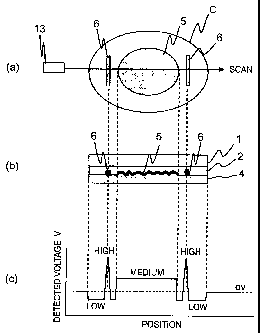
Fig. 1(a) shows the planar structure of an information
recording patch according to the first embodiment. Fig. 1(b)
shows the longitudinal sectional structure.
CA 02638006 2008-07-22
12
An information recording patch A has a conductive region
and a dielectric region and includes a protective layer 1,
intermediate layer 2, metal layer 3, and adhesive layer 4. The
intermediate layer 2 is embossed. The intermediate layer 2
and the metal layer 3 stacked on it form a hologram layer.
Since the metal layer 3 is formed on the surface of the
intermediate layer 2 with the three-dimensional pattern, the
hologram has a function of generating an image that optically
changes in accordance with the three-dimensional pattern when
light that has entered from the protective layer side is visually
recognized as it is reflected by the metal layer 3 and passes
through the protective layer 1 again.
In this embodiment, the shape of the three-dimensional
pattern of the intermediate layer 2 and the degree of the optical
change do not influence mechanical reading. Hence, a detailed
description of the optical change will be omitted. If the
intermediate layer 2 has no three-dimensional pattern, the
intermediate layer 2 and the metal layer 3 which are simply
stacked do not serve as a hologram having the function of
causing an optical change. However, they have the function of
an information recording medium and are usable as an
information recording patch by a metal foil.
The layers included in the information recording patch
according to this embodiment will be described next.
In the information recording patch A, the protective layer
1, intermediate layer 2, and adhesive layer 4 use dielectrics
having predetermined dielectric constants. The metal layer 3
uses a conductive material having a predetermined conductivity.
In this embodiment, the metal layer 3 is arranged in a circular
shape in the conductive region. The protective layer 1,
intermediate layer 2, and adhesive layer 4 are arranged in an
elliptical shape larger than the metal layer 3.
Fig. 1(c) shows a detected voltage upon reading, using a
sensor, the information recording patch A pasted to, e.g., an
article of value via the adhesive layer.
The detected voltage in the dielectric region
CA 02638006 2008-07-22
13
corresponding to the portion of the protective layer 1,
intermediate layer 2, and adhesive layer 4 arranged in an
elliptical shape larger than the metal layer 3 has a level lower
than 0 V of the base. The detected voltage in the conductive
region corresponding to the metal layer portion has a level
higher than 0 V of the base.
Hence, in confirming the authenticity of the information
recording patch pasted to, e.g., an article of value, the
information recording patch can be discriminated as authentic
only when two conditions are satisfied upon reading using the
sensor: the elliptical dielectric region is detected, and the
circular conductive region is detected at a predetermined
position in the ellipse.
In this embodiment, the dielectric region that forms the
information recording patch is elliptic, and the conductive region
is circular. However, the present invention is not limited to this,
and they can have any shape as far as the conductive region is
surrounded by the dielectric region. The two regions may be
adjacent to each other.
Figs. 2(a) and 2(b) show the structure of an information
recording patch according to the second embodiment.
An information recording patch B has conductive regions
and a dielectric region and includes a protective layer 1,
intermediate layer 2, metal layers 5 and 6, and adhesive layer 4.
The protective layer 1, intermediate layer 2, and adhesive layer
4 use dielectrics having predetermined dielectric constants.
The metal layers use a conductive material having a
predetermined conductivity.
In this embodiment, metal layers are arranged in two
kinds of shapes. The first metal layer 5 is arranged in a
circular shape in the conductive region, whereas the second
metal layers 6 are arranged in a crescent shape on both sides of
the first metal layer 5. The protective layer 1, intermediate
layer 2, and adhesive layer 4 are arranged in an elliptical shape
larger than the metal layers. That is, in this embodiment, a
total of three metal layers, i.e., one circular shape and two
CA 02638006 2008-07-22
14
crescent shapes are arranged in the conductive regions.
Fig. 2(c) shows detected voltages upon reading, using a
sensor, the information recording patch B pasted to, e.g., an
article of value via the adhesive layer. The detected voltage in
the dielectric region corresponding to the portion of the
protective layer 1, intermediate layer 2, and adhesive layer 4
arranged in an elliptical shape larger than the first metal layer 5
and the second metal layers 6 has a level lower than 0 V of the
base. The detected voltages in the conductive regions
corresponding to the first and second metal layer portions have
the same level higher than 0 V of the base.
Hence, in confirming the authenticity of the information
recording patch, the information recording patch can be
discriminated as authentic only when three conditions are
satisfied upon reading using the sensor: the elliptical dielectric
region is detected, the circular conductive region is detected at
a predetermined position in the ellipse, and crescent conductive
regions are detected at predetermined positions in the ellipse.
Figs. 3(a) and 3(b) show the structure of an information
recording patch according to the third embodiment. An
information recording patch C has conductive regions and a
dielectric region and includes a protective layer 1, intermediate
layer 2, metal layers 5 and 6, and adhesive layer 4. The
protective layer 1, intermediate layer 2, and adhesive layer 4
use dielectrics having predetermined dielectric constants. The
metal layers 5 and 6 use a conductive material having a
predetermined conductivity.
In this embodiment, metal layers are arranged in two
kinds of shapes. The first metal layer 5 is arranged in a
circular shape in the conductive region, whereas the second
metal layers 6 are arranged, on both sides of the first metal
layer 5, in a shape having a width and length that cause
resonance with a predetermined frequency upon measuring
using a microwave sensor. The protective layer 1, intermediate
layer 2, and adhesive layer 4 are arranged in an elliptical shape
larger than the metal layers.
CA 02638006 2008-07-22
To make the second metal layers 6 resonate with a
predetermined frequency, the length of the long side must be
1/2" (n is an integer: n >_ 0) of a predetermined wavelength.
To cause resonance, the second metal layer 6 preferably
5 has an anisotropic shape such as a rectangular or elliptical
shape.
That is, in this embodiment, a total of three metal layers,
i.e., one circular shape and two shapes each having a width and
length that cause resonance with a frequency are arranged in
10 the conductive regions.
Fig. 3(c) shows detected voltages upon reading, using a
sensor, the information recording patch C pasted to, e.g., an
article of value via the adhesive layer. The detected voltage in
the dielectric region corresponding to the portion of the
15 protective layer 1, intermediate layer 2, and adhesive layer 4
arranged in an elliptical shape larger than the metal layers 5
and 6 has a level lower than 0 V of the base. The detected
voltage in the conductive region of the first metal layer 5 has a
level higher than 0 V of the base. The detected voltage in the
conductive region of each second metal layer 6 has a level
higher than that of the first metal layer 5.
Hence, in confirming the authenticity of the information
recording patch, the information recording patch can be
discriminated as authentic only when three conditions are
satisfied upon reading using the sensor: the elliptical dielectric
region is detected, the circular conductive region is detected at
a predetermined position in the ellipse, and the two conductive
regions each having a width and length that cause resonance
with the frequency of the sensor are detected at predetermined
positions in the ellipse.
Figs. 4(a) and 4(b) show the structure of an information
recording patch according to the fourth embodiment. An
information recording patch D includes a protective layer 1,
intermediate layer 2, metal layer 3, and adhesive layer 4. The
protective layer 1, intermediate layer 2, and adhesive layer 4
use dielectrics having predetermined dielectric constants. The
CA 02638006 2008-07-22
16
metal layer 3 uses a conductive material having a
predetermined conductivity.
In this embodiment, the metal layer is arranged in a
circular shape in the conductive region while including
nonconductive regions 7 formed by partially removing the metal
layer 3. The protective layer 1, intermediate layer 2, and
adhesive layer are arranged in an elliptical shape larger than
the metal layer 3. The portions of the nonconductive regions 7
in the metal layer 3 are made of only dielectrics.
Fig. 4(c) shows detected voltages upon reading, using a
sensor, the information recording patch D pasted to, e.g., an
article of value via the adhesive layer. The detected voltage in
the dielectric region corresponding to the portion of the
protective layer 1, intermediate layer 2, and adhesive layer 4
arranged in an elliptical shape larger than the metal layer 3 has
a level lower than 0 V of the base. The detected voltage of the
metal layer 3 has a level higher than 0 V of the base. The
detected voltage of each nonconductive region 7 in the metal
layer 3 has the same level as in the dielectric region that is
lower than 0 V of the base.
Hence, in confirming the authenticity of the information
recording patch, the information recording patch can be
discriminated as authentic only when three conditions are
satisfied upon reading using the sensor: the elliptical dielectric
region is detected at a predetermined position, the circular
conductive region is detected at a predetermined position in the
ellipse, and the dielectric regions corresponding to the
nonconductive regions are detected at predetermined positions
in the circle.
Fig. 5 shows the structure of an information recording
patch according to the fifth embodiment. An information
recording patch E shown in Figs. 5(a) and 5(b) includes a
protective layer 1, intermediate layer 2, metal layers 5 and 6,
and adhesive layer 4. The protective layer 1, intermediate
layer 2, and adhesive layer 4 use dielectrics having
predetermined dielectric constants. The metal layers 5 and 6
CA 02638006 2008-07-22
17
use a conductive material having a predetermined conductivity.
In this embodiment, the metal layers are formed by
combining vertical strips and horizontal stripes. The first metal
layer 5 is arranged as a combination of horizontal stripes. The
second metal layer 6 is arranged as a combination of vertical
stripes. The protective layer 1, intermediate layer 2, and
adhesive layer 4 are arranged in an elliptical shape larger than
the image of the metal layers. The vertical and horizontal
stripes made of the metal layers are conductive. Portions
between the vertical stripes or horizontal stripes are dielectric
because of the absence of the metal layers.
The length of the long side of the second metal layer 6
must be 1/2" of a predetermined wavelength. To cause
resonance, the second metal layer 6 preferably has an
anisotropic shape. The second metal layer 6 is rectangular
here. However, the second metal layer 6 need not always have
a rectangular shape and may have an elliptical shape or the
like.
Fig. 5(c) shows detected voltages upon reading, using a
sensor, the information recording patch E pasted to, e.g., an
article of value via the adhesive layer. The detected voltage in
the dielectric region corresponding to the portion of the
protective layer 1, intermediate layer 2, and adhesive layer 4
arranged in an elliptical shape larger than the metal layers has
a level lower than 0 V of the base. The detected voltage in the
conductive region of the first metal layer 5 formed from
horizontal stripes has a level higher than 0 V of the base. The
detected voltage of the second metal layer 6 formed from
vertical stripes has a level higher than that of the first metal
layer 5 at each layer portion corresponding to a vertical stripe
and a level lower than 0 V of the base at each dielectric region
portion between the stripes.
Hence, in confirming the authenticity of the information
recording patch, the information recording patch can be
discriminated as authentic only when three conditions are
satisfied upon reading using the sensor: the elliptical dielectric
CA 02638006 2008-07-22
18
region is detected, the conductive regions having vertical and
horizontal stripe patterns are detected at predetermined
positions in the ellipse, and dielectric regions are detected
between the stripes at predetermined positions in the ellipse.
(Form of Information Recording Patch)
The six elements of the third and fifth embodiments, i.e.,
the metal layer, the metal layer having a width and length that
cause resonance with a frequency upon measuring using a
microwave sensor, the protective layer, the intermediate layer,
the adhesive layer, and the nonconductive region formed by
partially removing the conductive region are measured using a
microwave sensor. Then, the six elements are classified into
the following three levels (a) to (c).
a) Dielectric level (I ow level): protective layer,
intermediate layer, adhesive layer, and nonconductive region
formed by partially removing the conductive region
b) First conductive level (medium level): metal layer
(conductive region)
c) Second conductive level (high level): metal layer (the
portion that resonates with a predetermined wavelength upon
measuring using a microwave sensor)
The information recording patch according to each of the
third and fifth embodiments carries information by appropriately
arranging the six elements and the three levels (a) to (c) in a
combination of (a) and (b), (a) and (c), or (a), (b), and (c).
To apply the information recording patch to a base
material or the like, for example, the following three methods
are available.
(a) Direct Applying Method
The protective layer, intermediate layer, adhesive layer,
and metal layer are directly applied to a base material. The
protective layer, intermediate layer, and adhesive layer can be
formed by forming a coating directly on a base material using
an applicator, coater, or various kinds of printing machines. For
stable mechanical reading, a method such as screen printing,
gravure printing, or intaglio printing capable of obtaining a large
CA 02638006 2008-07-22
19
ink transfer amount is preferable. The metal layer can be
formed directly on the base material using a vapor deposition
apparatus.
(b) Retransfer Method
A retransfer method used for an OVD or the like is
available, in which the materials are arranged on a transfer base
material and retransferred to a base material by, e.g., heat,
pressure, or adhesive. For stable mechanical reading, it is
preferable to form a uniform transfer film by thermal transfer
printing or hot stamping.
(c) Label Method
A label that is an adhesive sticker is pasted to a printed
product or the like together with the base material. To do this,
a method is available, in which the materials are arranged on a
label base material and pasted to a base material by, e.g., an
applied adhesive. For stable mechanical reading, it is
preferable to form a uniform transfer film by thermal transfer
printing or hot stamping.
The thickness of the conductive layer is preferably 400 to
2,000 A. If the conductive layer is thinner than 400 A, it is
difficult to obtain a sufficient voltage in detection by mechanical
reading. If the conductive layer is thicker than 2,000 A, the
flexibility of the hologram becomes slightly poor.
(Mechanical Reading Method)
Mechanical reading necessary for authenticity
discrimination of the information recording patch obtained by
each of the first to fifth embodiments will be described next.
(Explanation of Principles)
To read the information recording patch of each of the
first to fifth embodiments, it is necessary to use a mechanical
reading apparatus capable of detecting the conductivity and
dielectric constant. In this embodiment, mechanical reading
using a sensor using a microwave that is a band of an
electromagnetic wave will be described with reference to the
accompanying drawings. In this embodiment, the
electromagnetic wave has a frequency of 3 kHz (exclusive) to
CA 02638006 2008-07-22
30 THz (inclusive) as defined in the Radio Wave Act. For
example, a microwave having a frequency of 1 GHz to 300 GHz
is preferable.
Fig. 6(a) shows an example of the arrangement of a
5 sensor capable of simultaneously measuring a conductor and a
dielectric.
This sensor performs measurement by leaking a
microwave from a waveguide 8 and will therefore be called a
leakage microwave sensor 13. The leakage microwave sensor
10 13 includes the waveguide 8, an irradiation means 9 for
irradiating the inside of the waveguide with an electromagnetic
wave, a receiving means 10, a leakage hole 11 formed in a wall
of the waveguide 8 to externally leak an electromagnetic wave
propagating through the waveguide, and a reflecting plate 14.
15 Fig. 6(b) shows an example of the internal structure of
the leakage microwave sensor 13 which performs measurement
by leaking a microwave from the waveguide 8. The leakage
microwave sensor 13 can detect the conductivity or dielectric
property of a sheet-shaped target measurement object 12.
20 The principles of the leakage microwave sensor 13 will be
described next.
Fig. 7 shows the main part of the leakage microwave
sensor 13. This part corresponds to the core of the function.
Fig. 7(a) shows a state in which the leakage hole 11 for leaking
an electromagnetic wave 15 is arranged in the upper wall of the
waveguide 8, and the electromagnetic wave 15 from the
electromagnetic wave oscillation source irradiates the inside of
the waveguide 8 so that an electromagnetic wave distribution in
a TE10 mode is obtained in the waveguide.
Fig. 7(b) shows a magnetic field distribution 16 of a
magnetic field in the waveguide and a magnetic field leaked
from the leakage hole 11. Fig. 7(c) shows an electric field
distribution 17 of an electric field in the waveguide and an
electric field leaked from the leakage hole 11. Fig. 7(d) shows
a principle that when a leaked electromagnetic field is
transmitted through the target measurement object 12 which is
CA 02638006 2008-07-22
21
placed on the leakage hole 11 while facing it, the magnetic field
distribution 16 or electric field distribution 17 in the waveguide
changes depending on the material properties of the target
measurement object 12.
In this case, when a portion such as a paper or resin
portion having a large dielectric constant comes to the leakage
hole 11, it affects the leaked electromagnetic field. Hence, the
amplitude or phase of a standing wave generated upon
synthesizing the electromagnetic wave propagating through the
waveguide 8 and the reflected electromagnetic wave changes.
When a portion such as a metal deposition film or crystal film
having a high conductivity comes to the leakage hole 11, the
material with the high conductivity blocks the leakage hole.
Hence, a cavity resonance state is generated in the waveguide 8,
and the amplitude or phase of the electromagnetic field
changes.
More specifically, the detected voltage obtained by
measurement exhibits a waveform including both the change by
the dielectric constant and the change by the conductivity. For
this reason, whether the target measurement material is a
conductor or a dielectric can be known based on the waveform
in measurement.
Principles that the target measurement object 12 is
placed on the apparatus and measured will be described next.
Fig. 8 shows a state in which the target measurement
object is placed on the apparatus and measured. Fig. 8(a)
shows a state in which the target measurement object 12 is not
present on the leakage hole 11. The detected voltage at this
time is defined as a first voltage (this level is considered as the
zero-base of the detected voltage).
Fig. 8(b) shows a state in which the target measurement
object 12 is placed on the leakage hole 11. The detected
voltage at this time is defined as a second voltage.
Figs. 9(a), 9(b), and 9(c) show the three classes of
detected voltages obtained upon measuring various kinds of
target measurement objects 12 in the order of Figs. 8(a) and
CA 02638006 2008-07-22
22
8(b).
Fig. 9(a) shows a voltage when the target measurement
object 12 is made of a PET film. The second voltage exhibited
a negative value based on the dielectric constant.
That is, when the target measurement object 12 is made
of a dielectric material, first voltage > second voltage.
Fig. 9(b) shows a voltage when the target measurement
object 12 is made of a metal layer formed by metal deposition
on a PET film. The target measurement object 12 was placed
on the leakage hole 11 and measured without being relatively
moved. Hence, the second voltage exhibited not a negative
value based on the dielectric constant of PET but only a positive
value based on the metal layer having a high conductivity.
That is, when the target measurement object 12 made of
a composite material of a dielectric material and a conductive
material is measured without conveyance, first voltage < second
voltage.
Fig. 9(c) shows a voltage when the target measurement
object 12 is made of an aluminum foil (a general aluminum foil
for domestic use). The second voltage exhibited a positive
value based on the conductivity.
That is, when the target measurement object 12 is made
of a conductive material, first voltage < second voltage.
The components of the leakage microwave sensor will be
described next.
As shown in Fig. 10, the sensor comprises the irradiation
means 9 including a transmitting antenna 18 and a transmitting
diode 19 such as a Gunn diode, the receiving means 10
including a receiving antenna 21 and a receiving diode 22 such
as a Schottky diode, the waveguide 8 having the leakage hole
11 in the upper wall, and the reflecting plate 14 to close the
waveguide 8.
The transmitting diode 19 irradiates the inside of the
waveguide with an electromagnetic wave in a TE10 mode via
the transmitting antenna 18. The electromagnetic field
partially externally leaks from the leakage hole 11. When the
CA 02638006 2008-07-22
23
target measurement object 12 is placed on the leakage hole 11,
the electromagnetic field is transmitted through the target
measurement object 12. The amplitude or phase of the
electromagnetic wave in the waveguide changes depending on
the material properties of the target measurement object. The
receiving diode 22 detects the change via the receiving antenna
21 to discriminate the material of the target measurement
object on the basis of the change amount.
As for adjustment of the apparatus, the positions of the
leakage hole 11 and reflecting plate 14 relative to a microwave
transmitting/receiving unit 20 are important to most leak the
electromagnetic wave 15 in the waveguide from the leakage
hole 11. To enable measurement based on the conductivity,
the leakage hole and reflecting plate are preferably adjusted to
such positions that generate a cavity resonance state in the
waveguide when the conductor blocks the leakage hole 11.
In the example to be describe below, a Doppler module
used in an automatic door or speed sensor is used as a
component that serves as both the irradiation means 9 including
the transmitting antenna 18 and the transmitting diode 19 such
as a Gunn diode and the receiving means 10 including the
receiving antenna 21 and the receiving diode 22 such as a
Schottky diode. The Doppler module comprises the transmitting
diode 19, transmitting antenna 18, receiving diode 22, and
receiving antenna 21 in a square waveguide WR42 and can
transmit or receive an electromagnetic wave of 24.15 GHz in the
TE10 mode.
The leakage microwave sensor 13 is used here as the
mechanical reading sensor. However, any other sensor capable
of reading a conductor or a dielectric is usable.
Simultaneously with the voltage waveform measurement
using the leakage microwave sensor 13, a voltage waveform
may be measured using an optical sensor, capacitance sensor,
or eddy current sensor for the target measurement object 12.
In this case, the voltage waveform obtained from the leakage
microwave sensor 13 on the basis of the conductivity and
CA 02638006 2008-07-22
24
dielectric constant is compared with the voltage waveform with
or without an OVD obtained from the optical sensor, capacitance
sensor, or eddy current sensor. Authenticity discrimination is
done based on the difference between the waveforms.
Simultaneously with the voltage waveform measurement
using the leakage microwave sensor 13, the target
measurement object 12 may be irradiated with near infrared
light, and the waveform of the transmitted near infrared light
may be measured. The shielding characteristic of a radio wave
obtained from the leakage microwave sensor 13 is compared
with the non-transmittance of the light obtained from the
waveform of light. Authenticity discrimination is done based on
the difference between the waveforms.
A method of reading, using the leakage microwave sensor
13, a conductor formed into a length that causes resonance with
a frequency will be described next.
The conductor is formed into a desired length and/or a
desired width using a material having a high electric
conductivity and arranged to express information.
Fig. 11 is a graph showing the length of a metal layer
which resonates with a frequency plotted along the abscissa and
a microwave detected voltage plotted along the ordinate. The
microwave is an electromagnetic wave. Its frequency (GHz)
and waveform (mm) are given below.
wavelength k = c/f (c: velocity of light, f: frequency)
The resonant wavelength of the antenna for the
electromagnetic wave is a fraction of an integer of the
wavelength X. The value of the microwave detected voltage is
affected by various factors as described above. Microwave
detected voltages of smooth conductors having various lengths
were actually measured using a microwave transmitter/receiver
of 24.15 GHz.
According to the experiments, the highest microwave
detected voltage can be obtained from an about 4-mm long
conductor based on various factors, as shown in Fig. 11.
Because of the presence of various factors, in Examples 1 and 2,
CA 02638006 2008-07-22
the length of the smooth conductor was set to "almost" a
fraction of an integer of the electromagnetic wave wavelength.
According to the experiments, generally, the detected voltage of
a smooth conductor whose length was about 1/4 the wavelength
5 of the detection microwave was high. The maximum value of
the microwave detected voltage was observed at lengths
corresponding to 1/2" (n is an integer: n >_ 0), i.e., 1/2, 1/8,
1/16,....
Results obtained by measuring the information recording
10 patches shown in Figs. 1 to 5 described above using the leakage
microwave sensor 13 will be described next.
Fig. 1(c) shows the measurement result of the
information recording patch A in Figs. 1(a) and 1(b). The
detected voltage by the leakage microwave sensor 13 exhibited
15 "medium level" in the circular conductive region arranged in the
metal layer 3, and "low level" in the remaining portion formed
by the protective layer 1, intermediate layer 2, and adhesive
layer 4.
Fig. 2(c) shows the measurement result of the
20 information recording patch B in Figs. 2(a) and 2(b). The
detected voltage by the leakage microwave sensor 13 exhibited
"medium level" in the two kinds of conductive regions, i.e., the
circular and crescent conductive regions are arranged in the
metal layers 5 and 6, and "low level" in the remaining portion
25 formed by the protective layer 1, intermediate layer 2, and
adhesive layer 4.
Fig. 3(c) shows the measurement result of the
information recording patch C in Figs. 3(a) and 3(b). The two
kinds of conductive regions are arranged in the metal layers 5
and 6. The detected voltage by the leakage microwave sensor
13 exhibited "medium level" in the circular conductive region,
"high level" in the conductive regions that resonate with a
frequency, and "low level" in the remaining portion formed by
the protective layer 1, intermediate layer 2, and adhesive layer
4.
Fig. 4(c) shows the measurement result of the
CA 02638006 2008-07-22
26
information recording patch D in Figs. 4(a) and 4(b). The
detected voltage by the leakage microwave sensor 13 exhibited
"medium level" in the circular conductive region arranged in the
metal layer 3, "low level" in the nonconductive regions 7 formed
in the circular metal layer 3, and "low level" in the remaining
portion formed by the protective layer 1, intermediate layer 2,
and adhesive layer 4.
Fig. 5(c) shows the measurement result of the
information recording patch E in Figs. 5(a) and 5(b). The metal
layers 5 and 6 form combinations of vertical and horizontal
stripes. The detected voltage by the leakage microwave sensor
13 exhibited "high level" in each vertical stripe portion of the
second metal layer 6, "medium level" in each horizontal stripe
portion of the first metal layer 5, "low level" in portions between
the vertical and horizontal stripes, and "low level" in the
remaining portions formed by the protective layer 1,
intermediate layer 2, and adhesive layer 4. Although the second
metal layer 6 and the first metal layer 5 have the same stripe
pattern, the detected voltage of the second metal layer 6 is
higher because the length of each vertical stripe resonates with
the frequency of the leakage microwave sensor 13 used for the
measurement, and the sensor and the vertical stripes are
parallel to each other.
(Example 1)
Fig. 12 to 14 show an example of an identification card
with an information recording patch as Example 1 of the first to
fifth embodiments. Fig. 12 shows an authentic identification
card 23. Fig. 13 shows a forged product 24 of the identification
card. Fig. 14 shows detected voltages in mechanical reading.
Fig. 12(a) is a plan view showing an example of the
authentic product of the identification card. Fig. 12(b) shows
its section.
Printing is performed on a base material 26 to form an
ink layer 25. An elliptical information recording patch
according to the embodiment, which allows authenticity
discrimination, is pasted onto the ink layer 25.
CA 02638006 2008-07-22
27
The information recording patch includes the adhesive
layer 4, intermediate layer 2, first metal layers 5 and 5', second
metal layers 6, and protective layer 1.
The ink layer 25, base material 26, adhesive layer 4, and
protective layer 1 made of a polyethylene resin are dielectric.
The first metal layers 5 and 5' formed by aluminum vapor
deposition are conductive. The second metal layers 6 formed
by aluminum vapor deposition are conductive but have a size to
resonate with the frequency (24.15 GHz) of the leakage
microwave sensor 13 used for measurement, unlike the first
metal layers 5 and 5'. The first metal layers 5' each having a
length and width different from those of the second metal layers
6 that resonate with the sensor are appropriately arranged.
Fig. 12(b) shows the section of the authentic product.
The identification card 23 basically has the following four kinds
of layer structures as a whole.
(1) Base material, ink layer, protective layer,
intermediate layer, and adhesive layer
(2) Base material, ink layer, protective layer,
intermediate layer, adhesive layer, and first metal layer
(3) Base material, ink layer, protective layer,
intermediate layer, adhesive layer, and second metal layer
(4) Only base material and ink layer
When the identification card 23 having these four kinds of
layer structures is measured through each layer stack using a
leakage microwave sensor, the following detection levels are
obtained.
(1) Only dielectric layers --> low level
(2) Dielectric layers and first metal layer -> medium
level
(3) Dielectric layers and second metal layer high level
(4) Only dielectric layers -* low level
The contents of the respective layers of the identification
card 23 will be explained next.
A 0.3-mm thick PET film was used as the base material
26. Any other material having a desired conductivity or
CA 02638006 2008-07-22
28
dielectric constant is usable except for PET. The thickness is
preferably about 0.3 to 0.75 mm.
The ink layer 25 is formed to print a design on the card.
An ink having a desired conductivity or dielectric constant is
usable. Printing was performed to an ink thickness of about 1
m by offset printing.
When the ink layer 25 was actually measured by the
leakage microwave sensor 13, the detected voltage level was
much lower than that of the information recording patch portion.
Such a level is supposed to be negligible and have no effect in
Example 1.
In Example 1, the intermediate layer 2 was formed using
a 0.1-mm thick PET layer. A three-dimensional pattern for an
optical change in a hologram forming layer was formed.
For the adhesive layer 4 and the protective layer 1, a
material having a desired conductivity or dielectric constant can
be selected from existing materials.
The first metal layers 5 and 5' and the second metal
layers 6 were formed by depositing a metal on the intermediate
layer 2. The first metal layers 5 and 5' were designed to
exhibit "medium level", and the second metal layers 6 were
designed to exhibit "high level" upon measurement using the
leakage microwave sensor 13.
In Example 1, the first metal layers 5 and 5' and the
second metal layers 6 were formed by aluminum vapor
deposition to a film thickness of 500 A. However, any other
material such as chromium is also usable if a desired
conductivity can be obtained.
Each second metal layer 6 needs to have a size to obtain
a high level upon resonating with the frequency (24.15 GHz) of
the leakage microwave sensor 13 used for measurement. In
Example 1, each second metal layer 6 had a bar-like shape
having a 4-mm long side and a 0.1-mm short side.
The short side of the second metal layer 6 was set to 0.1
mm against a forgery method of cutting and pasting an
available aluminum foil. The width is preferably as small as
CA 02638006 2008-07-22
29
possible and is not limited to 0.1 mm.
Fig. 13(a) shows an example of the forged product 24 of
the identification card. Fig. 13(b) shows the section of the
forged product. The forged product 24 of the identification
card is formed by copying the authentic product shown in
Fig. 12 by a copying machine and pasting an available
aluminum foil 27 or the like.
As shown in the sectional view, a large difference from
the authentic product is that the intermediate layer 2 and
protective layer 1 of the information recording patch used in
Example 1 do not exist.
Fig. 14(a) shows an example of a discrimination
apparatus for discriminating the target measurement object 12.
This apparatus comprises the leakage microwave sensor 13,
oscilloscope 29, and conveyor 28.
This discrimination apparatus causes the conveyor 28 to
convey target measurement objects, i.e., the authentic
identification card 23 shown in Fig. 12(a) and the forged
product 24 shown in Fig. 13(a) and causes the leakage
microwave sensor 13 to read them.
The conveyor 28 conveys the identification card 23
sandwiched between conveyor belts arranged on the upper and
lower sides at a conveyance speed of 2 m/sec to the leakage
microwave sensor 13. The leakage microwave sensor 13 is
arranged at a position to measure the information recording
patch pasted portion of the moving identification card 23 that is
being conveyed. The oscilloscope 29 can display the waveform
of a detected voltage scanned and measured by the leakage
microwave sensor 13. The forged product 24 of the
identification card is also measured in the same way.
In Example 1, measurement is done using the leakage
microwave sensor 13. However, any other measurement
apparatus capable of discriminatingly reading the nonconductive
region, first metal layer 5, and second metal layer 6 is usable.
Fig. 14(b) shows a detected voltage waveform obtained
by measuring the authentic identification card 23.
CA 02638006 2008-07-22
As can be seen from the waveform, three kinds of
detection levels were obtained in the respective portions,
including "low level" in the region having only the dielectrics,
"medium level" in the region of the dielectrics and the first
5 metal layer 5 or 5', and "high level" in the region of the
dielectrics and the second metal layer 6. The identification
card can be regarded as authentic based on Fig. 12(b) described
above.
On the other hand, Fig. 14(c) shows a detected voltage
10 waveform obtained by measuring the forged product 24. As
can be seen from the waveform, two kinds of detection levels
were obtained in the respective portions, including "medium
level" in the region of the dielectrics and the first metal layer 5,
and "high level" in the region of the dielectrics and the second
15 metal layer 6. However, since the detected voltage level in the
region having only the dielectrics was not low but zero, the
identification card can be regarded as a forged product. In this
way, it is possible to discriminate the authenticity based on the
layer structure of the hologram.
20 (Example 2)
Fig. 15 shows Example 2 in which an information
recording patch is applied to a cash voucher. In Example 1,
two detection levels are obtained by causing the first metal
layer 5 and second metal layer 6 of the information recording
25 patch to have different lengths. In Example 2, a high-level
detected voltage is obtained by changing the length of the
second metal layer 6 and additionally by making the direction of
the leakage microwave sensor 13 relatively parallel to a pattern
formed by arranging a conductive material in stripes.
30 A cash voucher 30 shown in Fig. 15(a) is formed by
printing its face value on a base material to form the ink layer
25, and pasting, onto the ink layer, a discrimination label 32
that is a metal foil having a rectangular shape and capable of
recording information. The metal foil includes the adhesive
layer 4, first metal layer 5, second metal layer 6, and base
material layer 26. The ink layer 25, paper sheet 31, adhesive
CA 02638006 2008-07-22
31
layer 4, and base material layer 26 are dielectric. The first
metal layer 5 formed by aluminum vapor deposition is
conductive. The second metal layer 6 formed by aluminum
vapor deposition is conductive but has a design to resonate with
the frequency (24.15 GHz) of the leakage microwave sensor 13
used for measurement, unlike the first metal layer 5.
Fig. 15(b) shows a section which basically has the
following four kinds of layer structures.
(1) Paper sheet, ink layer, base material layer, and
adhesive layer
(2) Paper sheet, ink layer, base material layer, adhesive
layer, first metal layer
(3) Paper sheet, ink layer, base material layer, adhesive
layer, second metal layer
(4) Only paper sheet and ink layer
When these four kinds of layer structures are measured
through each layer stack using a leakage microwave sensor, the
following detection levels are obtained.
(1) Only dielectric layers ---> low level
(2) Dielectric layers and first metal layer --> medium
level
(3) Dielectric layers and second metal layer high level
(4) Only dielectric layers -3 low level
The contents of the respective layers of the cash voucher
will be explained next.
A 0.1-mm thick bond paper sheet was used as the paper
sheet 31. Any other material having a desired conductivity or
dielectric constant is usable except for the bond paper sheet.
The ink layer 25 is formed by printing necessary
information such as a face value on the paper sheet 31. An ink
having a desired conductivity or dielectric constant is usable.
In Example 2, printing was performed to an ink thickness of
about 1 m by offset printing. When the printed portion was
actually measured by the leakage microwave sensor 13, the
detected voltage level was much lower than that of the portion
of the discrimination label 32. Such a level is supposed to be
CA 02638006 2008-07-22
32
negligible and have no effect in Example 2.
In Example 2, the base material layer was formed using a
0.1-mm thick PET film.
For the adhesive layer 4, a material having a desired
conductivity or dielectric constant can be selected from existing
materials.
The first metal layer 5 and the second metal layer 6 were
formed by aluminum vapor deposition on the base material
layer 26. The first metal layer 5 is designed to exhibit
"medium level", and the second metal layer 6 was designed to
exhibit "high level" upon measurement using the leakage
microwave sensor 13. In Example 2, the first metal layer 5 and
the second metal layer 6 were formed by aluminum vapor
deposition to a film thickness of 500 A. However, any other
material such as chromium is also usable if a desired
conductivity can be obtained.
Fig. 15(a) shows examples of designs applicable to the
first metal layer 5 and the second metal layer 6. The second
metal layer 6 has a design that resonates with the frequency
(24.15 GHz) of the leakage microwave sensor 13 used for
measurement to obtain a high level. An example is indicated
by a portion a in Fig. 15(a). The portion a in Fig. 15(a) is
formed by arranging 20 bars of a conductive material, each
having a length of 4 mm and a width of 0.1 mm, in a stripe
pattern at an interval of 0.1 mm. When the portion a relatively
parallel to the leakage microwave sensor is read, a high-level
detected voltage is obtained.
The first metal layer 5 has a design that does not
resonate with the frequency (24.15 GHz) of the leakage
microwave sensor 13 used for measurement to obtain a medium
Ievel. Examples of the first metal layer 5 are indicated by
portions b, c, d, and e in Fig. 15(a).
The portion b in Fig. 15(a) will be described in detail.
The portion b is formed by arranging 20 bars each having a
length of 4 mm and a width of 0.1 mm in a stripe pattern at an
interval of 0.1 mm and also superimposing a stripe pattern
CA 02638006 2008-07-22
33
perpendicularly intersecting the 20 stripes so that no resonance
with the frequency occurs. When the portion b is read by the
leakage microwave sensor, no resonance occurs, and a
medium-level detected voltage is obtained. That is, the portion
b in Fig. 15(a) apparently resembles the portion A. However,
the portion b does not resonate with the frequency, and only a
medium level is obtained. The medium level is easier to obtain
as the number of bars that are made of a conductive material
and arranged relatively perpendicular to the sensor increases.
This is because the pattern becomes almost solid, as indicated
by d.
The portions c, d, and e shown in Fig. 15(a) also
apparently resemble the portion a. However, they do not
resonate with the frequency, and only a medium level is
obtained because the portion c has a zigzag design, the portion
d is solid, and the portion e includes bars that are made of a
conductive material and arranged in a stripe pattern relatively
perpendicular to the sensor.
Fig. 15(c) shows a result obtained by causing the
conveyor 28 to convey the cash voucher 30 and causing the
leakage microwave sensor 13 to read it. In reading, the
apparatus shown in Fig. 14(a) was used.
When scanning measurement was done, a waveform
shown in Fig. 15(c) was obtained. The waveform was
compared with threshold level 1 and threshold level 2 to classify
the respective portions of the discrimination label 32 into three,
high, medium, and low levels. The portion a corresponding to
the second metal layer 6 in Fig. 15(a) exhibited "high level", the
portions b, c, d, and e corresponding to the first metal layer 5
exhibited "medium level", and the portion including only the
base material layer 26 and the adhesive layer 4 without the
metal layers 5 and 6 exhibited "low level". The levels are "high,
medium, medium, medium, medium" in the scanning direction.
They are replaced with "1" and "0" to obtain "10000". This will
be referred to as detection data.
When the detection data was collated with a preset
CA 02638006 2008-07-22
34
relationship between detection data and voucher types (table in
Fig. 15(d)), the face value of the cash voucher was
discriminated as y10,000.
The information recording patch of Example 2 is created
aiming at mechanically reading the face value of the cash
voucher and also as a measure against a forgery method of
cutting and pasting, e.g., an available aluminum foil. Hence,
the cut width is not limited to 0.1 mm in Example 2 and is
preferably smaller.
A basic authenticity discrimination method for various
articles of value with information recording patches will be
explained next.
(Example 3)
Figs. 16 and 17 show, as Example 3, examples of an
identification card with the information recording patch
described in the first embodiment. Fig. 16 shows the authentic
identification card 23. Fig. 17 shows the forged product 24 of
the membership card.
Fig. 16(a) is a plan view showing an example of the
authentic product of the identification card. Fig. 16(b) shows
its section. Printing is performed on the base material 26 to
form the ink layer 25. The elliptical information recording
patch A according to the embodiment, which allows authenticity
discrimination, is pasted onto the ink layer 25.
The information recording patch includes the adhesive
layer 4, intermediate layer 2, metal layer 3, and protective layer
1.
The ink layer 25, base material 26, adhesive layer 4, and
protective layer 1 made of a polyethylene resin are dielectric.
The metal layer 3 formed by aluminum vapor deposition is
conductive.
Fig. 16(b) shows the section of the authentic product.
The identification card 23 basically has the following three kinds
of layer structures as a whole.
(1) Base material, ink layer, protective layer,
intermediate layer, and adhesive layer
CA 02638006 2008-07-22
(2) Base material, ink layer, protective layer,
intermediate layer, adhesive layer, and metal layer
(3) Only base material and ink layer
When the identification card 23 having these three kinds
5 of layer structures is measured through each layer stack using a
leakage microwave sensor, the following detection levels are
obtained.
(1) Only dielectric layers -* low level
(2) Dielectric layers and metal layer -> medium level
10 The contents of the respective layers of the identification
card 23 will be explained next.
A 0.3-mm thick PET film was used as the base material
26. Any other material having a desired conductivity or
dielectric constant is usable except for PET. The thickness is
15 preferably about 0.3 to 0.75 mm. The ink layer 25 is formed to
print a design on the card. An ink having a desired
conductivity or dielectric constant is usable. Printing was
performed to an ink thickness of about 1 m by offset printing.
When the ink layer 25 was actually measured by the
20 leakage microwave sensor 13, the detected voltage level was
much lower than that of the information recording patch portion.
Such a level is supposed to be negligible and have no effect in
Example 3.
In Example 3, the intermediate layer 2 was formed using
25 a 0.1-mm thick PET layer. A three-dimensional pattern for an
optical change in a hologram forming layer was formed. For
the adhesive layer 4 and the protective layer 1, a material
having a desired conductivity or dielectric constant can be
selected from existing materials. The metal layer 3 is formed
30 by depositing a metal on the intermediate layer 2 and exhibits
"medium level" upon measurement using the leakage
microwave sensor 13.
In Example 3, the metal layer 3 was formed by aluminum
vapor deposition to a film thickness of 500 A. However, any
35 other material such as chromium is also usable if a desired
conductivity can be obtained.
CA 02638006 2008-07-22
36
Fig. 17(a) shows an example of the forged product 24 of
the identification card. Fig. 17(b) shows the section of the
forged product. The forged product 24 of the identification
card is formed by copying the authentic product shown in
Fig. 16 by a copying machine and pasting the available
aluminum foil 27 or the like. As shown in the sectional view, a
large difference from the authentic product is that the
intermediate layer 2 and protective layer 1 of the information
recording patch A used in Example 3 do not exist.
The discrimination apparatus shown in Fig. 14(a) causes
the conveyor 28 to convey target measurement objects, i.e., the
authentic identification card 23 shown in Fig. 16(a) and the
forged product 24 shown in Fig. 17(a) and causes the leakage
microwave sensor 13 to read them.
The conveyor 28 conveys the identification card
sandwiched between conveyor belts arranged on the upper and
lower sides at a conveyance speed of 2 m/sec to the leakage
microwave sensor 13. The leakage microwave sensor 13 is
arranged at a position to measure the information recording
patch pasted portion of the moving identification card 23 that is
being conveyed. The oscilloscope 29 can display the waveform
of a detected voltage scanned and measured by the leakage
microwave sensor 13. The forged product 24 of the
identification card is also measured in the same way.
In Example 3, measurement is done using the leakage
microwave sensor 13. However, any other measurement
apparatus capable of discriminatingly reading the nonconductive
region and the metal layer 3 is usable.
Fig. 16(c) shows a detected voltage waveform al
obtained by measuring the authentic identification card 23. As
can be seen from the waveform, two kinds of detection levels
were obtained in the respective portions, including "low level" in
the region having only the dielectrics, and "medium level" in the
region of the dielectrics and the metal layer 3. Hence, the
identification card can be regarded as authentic.
On the other hand, Fig. 17(c) shows a detected voltage
CA 02638006 2008-07-22
37
waveform a2 obtained by measuring the forged product 24. As
can be seen from the waveform, two kinds of detection levels
were obtained in the respective portions, including "low level" in
the region having only the dielectrics, and "medium level" in the
region of the dielectrics and the metal layer 3. However, since
the detected voltage level in the region having only the
dielectrics was not low, as in Fig. 16(c), but zero, the
identification card can be regarded as a forged product. That is,
it is possible to discriminate the forged product 24 based on the
absence of the protective layer 1, intermediate layer 2, and
adhesive layer 4 around the aluminum layer 27 or the like.
As described above, according to the first to fifth
embodiments of the present invention, it is possible to reliably
discriminate a forged product formed by a metallization
technique. Additionally, even when a mechanical authenticity
discrimination apparatus having a conveyance system produces
conveyance disturbance or noise, stable authenticity
discrimination is possible.
Even when a hologram or the like is formed on the
information recording patch, it is very difficult to forge it or alter
the data by using all materials because conductive regions,
dielectric regions, and metal adhered regions each having a
width and length that cause resonance with the frequency of the
microwave sensor are appropriately arranged.
Fig. 18 shows an information recording patch according
to the sixth embodiment of the present invention. A first
conductive region has a long side with a length to cause
resonance with the frequency of a microwave sensor. A second
conductive region has a size not to cause resonance with the
frequency of a microwave sensor. The second conductive
region is formed into a grid pattern, mesh pattern, mesh-like
pattern made formed from minute dots, or arbitrary pattern by
using hollow lines to change the conductivity.
An information recording patch F includes a protective
layer 104, intermediate layer 105, metal layer 106, and
adhesive layer 107. The metal layer 106 is segmented by
CA 02638006 2008-07-22
38
hollow lines to form the first and second conductive regions.
A first conductive region 101 has a width and length that
cause resonance with the frequency of a leakage microwave
sensor. As shown in Fig. 18(c), an element having a vertical
size of 4 mm and a horizontal size of 1 mm is arranged. The
periphery of the element is defined by hollow lines. A second
conductive region 102 has a size that does not cause resonance
with the frequency of the leakage microwave sensor. This
region is formed into a grid pattern with 1 mm x 1 mm squares
segmented by hollow lines and carries information for
authenticity discrimination.
Each hollow line to form the first conductive region 101
and the second conductive region 102 is so thin as to be
invisible or hard to see. A three-dimensional pattern may be
formed on the intermediate layer 105 so that a holographic
image which optically changes is obtained by stacking the metal
layer 106 on the intermediate layer 105. If no optically
changing function is necessary, the information recording patch
can be used as that made of a smooth metal foil without a
three-dimensional pattern on the intermediate layer 105. The
adhesive layer 107 is necessary to paste the information
recording patch to a paper sheet or the like. The protective
layer 104 for protecting the surface may be omitted.
Fig. 18(d) shows a detected voltage upon reading the
information recording patch F using a leakage microwave sensor
103. A detected voltage waveform a3 exhibited "high level" in
the first conductive region 101 because of the resonance with
the frequency of the leakage microwave sensor 103 and "low
level" in the second conductive region 102 because of the
absence of resonance with the frequency of the leakage
microwave sensor 103. Since the detected voltage waveform
a3 exhibits a unique waveform, it is possible to determine
whether the information recording patch is authentic.
Fig. 19 shows the structure of an information recording
patch according to the seventh embodiment of the present
invention. An information recording patch G shown in
CA 02638006 2008-07-22
39
Fig. 19(a) includes a protective layer 104, intermediate layer
105, metal layer 106, and adhesive layer 107, as is apparent
from the sectional view of Fig. 19(b). The metal layer 106 is
segmented by hollow lines to form a first conductive region 101
having vertical lines and a second conductive region 102 having
horizontal lines.
The first conductive region 101 has a shape that causes
resonance with the frequency of a leakage microwave sensor
103. Three lines each having a width of 0.5 mm and a length
of 4 mm are arranged. The second conductive region 102 has
a shape that does not cause resonance with the frequency of
the leakage microwave sensor 103. A plurality of lines each of
which does not have a width of 0.5 mm and a length of 4 mm
are arranged in parallel. The intermediate layer 105, adhesive
layer 107, and protective layer 104 are the same as in the sixth
embodiment shown in Fig. 18.
Fig. 19(c) shows a detected voltage upon reading the
information recording patch G using the leakage microwave
sensor 103. A detected voltage waveform a4 exhibited "high
level" in the first conductive region 101 because of the
resonance with the frequency of the leakage microwave sensor
103 and "low level" in the second conductive region 102
because of the absence of resonance with the frequency of the
leakage microwave sensor 103. Since the detected voltage
waveform a4 has a unique waveform, it is possible to
discriminate the authenticity of the information recording patch.
As described in the sixth and seventh embodiments in
detail, the information recording patch is apparently uniformly
conductive but is finely segmented by hollow lines in fact.
When the information recording patch is read by the leakage
microwave sensor, a unique detected voltage waveform based
on the first conductive region and the second conductive region
is obtained. It is therefore possible to accurately discriminate
the authenticity.
To form the information recording patch, for example, the
following three methods are available.
CA 02638006 2008-07-22
(a) Direct Applying Method
In the direct applying method, the protective layer,
intermediate layer, and metal layer are directly applied to a
base material. The protective layer and intermediate layer can
5 be formed by forming a coating directly on a base material
using an applicator, coater, or various kinds of printing machines.
For stable mechanical reading, a method such as screen printing,
gravure printing, or intaglio printing capable of obtaining a large
ink transfer amount is preferable. The hollow lines to segment
10 the first conductive region 101 and the second conductive
region 102 can be formed by, e.g., placing a masking film and
performing vapor deposition using a vapor deposition apparatus.
(b) Retransfer Method
The materials are arranged on a transfer base material
15 and retransferred to a base material by, e.g., heat, pressure, or
(adhesive). For stable mechanical reading, it is preferable to
form a uniform transfer film by thermal transfer printing or hot
stamping.
(c) Label Method
20 The materials are arranged on a label base material and
pasted to a base material by, e.g., an applied adhesive. For
stable mechanical reading, it is preferable to form a uniform
transfer film by thermal transfer printing or hot stamping.
The thickness of the metal layer is preferably 400 to
25 2,000 A. If the conductive layer is thinner than 400 A, it is
difficult to obtain a sufficient voltage in detection by mechanical
reading. If the conductive layer is thicker than 2,000 A, the
flexibility of the hologram becomes slightly poor.
(Mechanical Reading Method)
30 A method of mechanically reading the information
recording patch obtained by each of the sixth and seventh
embodiments will be described next.
(Explanation of Principles)
To read the information recording patch of each of the
35 sixth and seventh embodiments, it is necessary to use a
mechanical reading apparatus capable of detecting the
CA 02638006 2008-07-22
41
conductivity and waveform resonance. The sensor for reading
the information recording patch of each of the sixth and seventh
embodiments is the same as the sensor for reading the
information recording patch of each of the first to fifth
embodiments, and a description thereof will not be repeated.
In Examples 4 to 8, reading is performed using a leakage
microwave sensor shown in Fig. 10. As shown in Fig. 10, a
Doppler module used in an automatic door or speed sensor is
used as a component that serves as both an irradiation means 9
and a receiving means 10. The Doppler module comprises a
transmitting diode 19, transmitting antenna 18, receiving diode
22, and receiving antenna 21 in a square waveguide WR42 and
can transmit or receive an electromagnetic wave of 24.15 GHz
in the TE10 mode.
In this embodiment, a leakage microwave sensor is used
as a mechanical reading sensor. However, any other sensor
capable of reading a conductor or a dielectric is usable. For
example, information of the information recording patch may be
read using a capacitance sensor to read a dielectric and an eddy
current sensor to read a conductor.
A method of reading, using the leakage microwave sensor,
a conductive layer formed into a length that causes resonance
with a frequency will be described next. The conductive layer
is formed into a desired length and a desired width using a
material having a high electric conductivity and arranged to
express information.
Fig. 20 is a graph showing the length of the pattern of
the first conductive region of a metal layer plotted along the
abscissa and a microwave detected voltage plotted along the
ordinate. The microwave is an electromagnetic wave. Its
frequency (GHz) and waveform (mm) are given below.
wavelength k = c/f (c: velocity of light, f: frequency)
The resonant wavelength of the antenna for the
electromagnetic wave is a fraction of an integer of the
wavelength X. The value of the microwave detected voltage is
affected by various factors as described above. Microwave
CA 02638006 2008-07-22
42
detected voltages of smooth conductors having various lengths
were actually measured using a microwave transmitter/receiver
of 24.15 GHz.
According to the experiments, the highest microwave
detected voltage can be obtained from an about 4-mm long
conductor based on various factors, as shown in Fig. 20.
Because of the presence of various factors, in Examples 4 to 8,
the length of the conductor was set to "almost" a fraction of an
integer of the electromagnetic wave wavelength. According to
the experiments, generally, the detected voltage of a smooth
conductor whose length was about 1/4 the wavelength of the
detection microwave was high. The maximum value of the
microwave detected voltage was observed at lengths
corresponding to 1/2" (n is an integer: n > 0), i.e., 1/2, 1/8,
1/16,....
Detailed Examples 4 to 8 using the information recording
patch will be described next.
(Example 4)
Fig. 21 shows, as Example 4, an example of the structure
of an identification card with an information recording patch and
a reading method therefor. Figs. 21(a) and 21(b), and 22(b)
show an information recording patch that allows authenticity
discrimination. Fig. 22(a) shows a reading apparatus.
Fig. 22(c) shows a detected voltage upon reading an authentic
identification card with the information recording patch in the
scanning direction. Figs. 23(b) and 24(b) show detected
voltages upon reading forged products shown in Figs. 23(a) and
24(a) by the reading apparatus, respectively.
An information recording patch 131 shown in Fig. 21(a)
includes the first conductive regions 101 each having a width
and length that cause resonance with the frequency of the
leakage microwave sensor, and the second conductive region
102 which does not resonate with the frequency and is formed
from the protective layer 104, intermediate layer 105, metal
layer (the first conductive layer 101 and the second conductive
layer 102), and adhesive layer 107.
CA 02638006 2008-07-22
43
Each first conductive region 101 was formed into a shape
having a width and length that cause resonance with the
frequency of the leakage microwave sensor. As shown in
Fig. 21(b), two elements each having a vertical size of 4 mm
and a horizontal size of 1 mm were arranged. The second
conductive region 102 was formed into a hollow grid or mesh
pattern not to resonate with the frequency of the leakage
microwave sensor. Blocks each having a vertical size of 1 mm
and a horizontal size of 1 mm were two-dimensionally arranged.
A three-dimensional pattern was formed on the
intermediate layer 105 so that the intermediate layer 105 and
the metal layer (the first conductive layer 101 and the second
conductive layer 102) stacked on it form a hologram layer, i.e.,
has a function of causing an optical change. The adhesive layer
107 is used to paste the information recording patch 131 to the
identification card. The protective layer 104 for protecting the
surface may be omitted.
Fig. 22(b) shows the structure of an identification card
123 of Example 4. The identification card 123 includes a base
material 124 for the identification card, an ink layer 125, and
the information recording patch 131.
Fig. 22(a) shows a state in which a conveyor 127 conveys
the identification card 123 with the information recording patch
131 to perform measurement. The leakage microwave sensor
103 is attached to the conveyor 127. An oscilloscope 112
displays the detected voltage of the leakage microwave sensor
103 upon conveying the identification card 123.
A 0.3-mm thick PET film was used as the base material
124 for the identification card. Any other material having a
desired dielectric constant is usable except for PET. The
thickness is preferably about 0.3 to 0.75 mm. The ink layer
125 formed by printing information and a design necessary for
the identification card has a desired dielectric constant.
Printing was performed to an ink thickness of about 1 m by
offset printing. The protective layer and the intermediate layer
were made of a polyethylene resin. In Example 4, the
CA 02638006 2008-07-22
44
intermediate layer was formed using a 0.1-mm thick PET film.
A three-dimensional pattern for an optical change in a hologram
was formed.
The first conductive regions and the second conductive
region of the information recording patch were formed by
depositing aluminum on the intermediate layer. Hollow lines
each having a width of 0.1 mm were formed by etching.
In Example 4, the first conductive regions and the second
conductive region were formed by aluminum vapor deposition to
a film thickness of 500 A. However, any other material such as
chromium is also usable if a desired conductivity can be
obtained.
The first conductive region were defined by the hollow
lines into a size (vertical size of 4 mm x horizontal size of 1
mm) that causes resonance with the frequency 24.15 GHz and
arranged on the left and right sides, respectively. The second
conductive region was segmented, by the hollow lines, into sizes
(grid pattern with 1 mm x 1 mm squares) that do not cause
resonance with the frequency 24.15 GHz. Each hollow line is
so thin as to be invisible or hard to see.
When the base material 124, ink layer 125, protective
layer 104, and intermediate layer 105 made of dielectric
materials were measured by the leakage microwave sensor 103,
the detected voltage level was much lower than that of the
information recording patch. Such a level is supposed to be
negligible and is therefor not taken into consideration in
Example 4.
Fig. 22(c) shows a detected voltage waveform a5
obtained by measuring the identification card using the
apparatus shown in Fig. 22(a). The waveform a5 exhibited
"high level" in the first conductive regions, "low level" in the
second conductive region, and about 0 V in portions of the
identification card 123 without the information recording patch.
It is therefore possible to discriminated the authenticity of the
identification card 123.
Fig. 23 shows an example of a forged product 128 of the
CA 02638006 2008-07-22
identification card. As shown in the sectional view, a color copy
layer 129 is formed on the base material 124 in place of the ink
layer of the authentic identification card, and an available
aluminum foil 130 is pasted via the adhesive layer 107 in place
5 of the metal layer of the information recording patch of the
authentic identification card. Fig. 23(b) shows a detected
voltage waveform a6.
The forged product is different from the authentic
identification card in two points. As one point, the metal layer
10 is thick. For this reason, the whole region of the hologram
exhibits "medium level" upon measurement using the leakage
microwave sensor 103. The other point is that the aluminum
foil 130 is not segmented by hollow lines, and the first
conductive regions 101 and the second conductive region 102 of
15 the authentic identification card do not exist. Hence, no region
resonates with the frequency (24.15 GHz) of the first conductive
region upon measurement using the leakage microwave sensor
103. Due to the two reasons, the forged product exhibits the
detected voltage waveform a6 upon measurement using the
20 leakage microwave sensor 103. It is therefore possible to
determine that the identification card is a forged product.
Fig. 24 shows another example of the forged product 128
of the identification card. As shown in the sectional view, the
color copy layer 129 is formed on the base material 124 in place
25 of the ink layer of the authentic identification card. Similarly, a
color copy layer is formed using a color copying machine in
place of the metal layer of the information recording patch of
the authentic identification card, thereby forging the
identification card.
30 Fig. 24(b) shows a detected voltage waveform a7.
The forged product is different from the authentic product
in the following points. That is, since no metal layer of
aluminum is present, the whole region of the hologram exhibits
about 0 V upon measurement using the leakage microwave
35 sensor 103. Additionally, since the first conductive regions 101
do not exist, no level resonant with the frequency (24.15 GHz)
CA 02638006 2008-07-22
46
is obtained. It is possible to determine on the basis of the two
differences that the identification card is a forged product.
(Example 5)
Fig. 25 shows another example of the identification card
123 with the information recording patch 131. The
identification card 123 includes the base material 124 for the
identification card, the ink layer 125, and the information
recording patch 131.
In Example 4, the information recording patch had a
mesh pattern formed by vertically arranging hollow lines in the
longitudinal direction and horizontally arranging hollow lines in
the lateral direction. In the information recording patch of
Example 5, hollow lines in the longitudinal direction and those in
the lateral direction were arranged obliquely. The second
conductive region 102 had a design as an aggregate of
rhombuses, whereas each first conductive region 101 was
designed by connecting some rhombuses to a length that causes
resonance with the leakage microwave sensor 103. Hence, as
compared to the information recording patch 131 of Example 4
shown in Fig. 22(b), the presence of the first conductive regions
101 is more hard to confirm.
Fig. 25(b) shows a detected voltage waveform a8. The
waveform a8 exhibited "high level" in the first conductive
regions 101, "low level" in the second conductive region 102,
and about 0 V in portions of the identification card 123 without
the information recording patch. It is therefore possible to
discriminate the authenticity of the identification card 123.
(Example 6)
Fig. 26 shows another example of an information
recording patch 126. In Example 6, the information recording
patch 126 including the protective layer 104, intermediate layer
105, and metal layer 106 can be pasted to a document or the
like via the adhesive layer 107.
The metal layer 106 is segmented by hollow lines to form
first conductive regions 101 each having vertical stripes and a
second conductive region 102 having horizontal stripes. Each
CA 02638006 2008-07-22
47
first conductive region 101 has a shape that causes resonance
with the frequency of the leakage microwave sensor 103.
Three lines each having a width of 0.5 mm and a length of 4
mm are arranged at two points. The second conductive region
102 has a shape that does not cause resonance with the
frequency of the leakage microwave sensor. A plurality of lines
each of which does not have a width of 0.5 mm and a length of
4 mm are arranged in parallel. Hence, the presence of the first
conductive regions 101 is hard to confirm.
Fig. 26(c) shows a detected voltage waveform a9. The
waveform a9 exhibited "high level" in the two first conductive
regions 101 and "low level" in the second conductive region 102.
It is therefore possible to determine that the information
recording patch 126 pasted to a document or the like is
authentic.
(Example 7)
Figs. 27 to 29 are views for explaining Example 7. After
reading using a leakage microwave sensor, reading is further
performed using an eddy current sensor capable of detecting a
material, thereby enhancing the authenticity discrimination
effect.
Fig. 27 shows the structure of the identification card 123
with the authentic information recording medium 131, a
detected voltage obtained by reading the identification card in
the scanning direction using a leakage microwave sensor, and a
detected voltage obtained by reading in the scanning direction
using an eddy current sensor.
Fig. 28 shows the structure of a forged identification card
formed by pasting the aluminum foil 130 to portions
corresponding to the first conductive regions of the authentic
information recording medium so as to obtain the same
detected voltage as in the authentic product by the leakage
microwave sensor, a detected voltage obtained by reading the
forged identification card in the scanning direction using a
leakage microwave sensor, and a detected voltage obtained by
reading in the scanning direction using an eddy current sensor.
CA 02638006 2008-07-22
48
The information recording medium shown in Fig. 27 has the
same structure as in Example 4.
Fig. 29 shows a reading apparatus using a leakage
microwave sensor and an eddy current sensor. Fig. 29 shows a
state in which the conveyor 127 conveys the identification card
123 with the information recording patch 131 to perform
measurement. The leakage microwave sensor 103 and an eddy
current sensor 132 are attached to the conveyor 127. The
oscilloscope 112 displays the detected voltages of the leakage
microwave sensor 103 and the eddy current sensor 132 upon
conveying the identification card 123.
A process of discriminating the identification card will be
described with reference to Fig. 27. A detected voltage
waveform alO shown in Fig. 27(b) is a result obtained by
measuring the identification card 123 conveyed by the conveyor
127 in Fig. 29 at the portion of the leakage microwave sensor
103. The waveform alO exhibited "high level" in the first
conductive regions that resonated with the microwave, "low
level" in the second conductive region that did not resonate,
and 0 V in portions without the information recording patch.
A detected voltage waveform all shown in Fig. 27(c) is a
result obtained by measuring the conveyed identification card
123 at the portion of the eddy current sensor 132 of the
conveyor 127 in Fig. 29. The detected voltage waveform all
exhibited "high level" all over the information recording medium
because the eddy current sensor 132 which reacts to a metal
detected both the first conductive regions 101 and the second
conductive region 102 of the information recording medium 131
of the identification card 123.
Fig. 28 explains a process of discriminating the forged
product 128 of the identification card. As shown in the
sectional view of Fig. 28(a), the color copy layer 129 is formed
on the base material 124 in place of the ink layer of the
authentic identification card, and the available aluminum foil
130 is pasted via the adhesive layer 107 in place of the first
conductive region metal layer of the authentic information
CA 02638006 2008-07-22
49
recording patch.
A detected voltage waveform a12 shown in Fig. 28(b) is a
result obtained by measuring the forged product 128 at the
portion of the leakage microwave sensor 103 of the reading
apparatus shown in Fig. 29. The waveform a12 exhibited "high
level" in portions corresponding to the first conductive regions
of the authentic product because of the aluminum foil 130,
about 0 V in a portion corresponding to the second conductive
region of the authentic product because nothing existed, and 0
V in portions without the information recording patch.
A detected voltage waveform a13 shown in Fig. 28(c) is a
result obtained by measuring the forged product at the portion
of the eddy current sensor 132 of the reading apparatus in
Fig. 29. The eddy current sensor 132 which reacts to a metal
detected the aluminum foil 130 corresponding to each first
conductive region of the authentic information recording
medium. However, since nothing existed in the portion
corresponding to each first conductive region, the waveform
exhibited 0 V.
As described above, as the method of discriminating the
authenticity of the identification card with the information
recording patch, the leakage microwave sensor 103 is used as
the first sensor of the reading apparatus, and the eddy current
sensor 132 is used as the second sensor to detect that, in an
authentic product, the pasted information recording medium has
conductivity in the whole region and partially resonates with a
microwave. This allows to more accurately discriminate the
authenticity of the identification card 123.
(Example 8)
Figs. 30 to 32 are views for explaining Example S. After
reading using a leakage microwave sensor, reading is further
performed using a transmission infrared sensor capable of
detecting a light transmission amount, thereby, enhancing the
authenticity discrimination effect.
Fig. 30 shows the structure of the identification card 123
with the authentic information recording medium 131, a
CA 02638006 2008-07-22
detected voltage obtained by reading the identification card in
the scanning direction using a leakage microwave sensor, and a
detected voltage obtained by reading in the scanning direction
using a transmission infrared sensor 133.
5 Fig. 31 shows the structure of a forged identification card
formed by pasting the aluminum foil 130 to portions
corresponding to the first conductive regions of the authentic
information recording medium so as to obtain the same
detected voltage as in the authentic product by the leakage
10 microwave sensor, a detected voltage obtained by reading the
forged identification card in the scanning direction using a
leakage microwave sensor, and a detected voltage obtained by
reading in the scanning direction using the transmission infrared
sensor 133. The information recording medium shown in
15 Fig. 30 has the same structure as in Example 4.
Fig. 32 shows a reading apparatus using a leakage
microwave sensor and the transmission infrared sensor 133.
Fig. 32 shows a state in which the conveyor 127 conveys the
identification card 123 with the information recording patch 131
20 to perform measurement. The leakage microwave sensor 103
and the transmission infrared sensor 133 are attached to the
conveyor 127. The oscilloscope 112 displays the detected
voltages of the leakage microwave sensor 103 and the
transmission infrared sensor 133 upon conveying the
25 identification card 123.
A process of discriminating the identification card will be
described with reference to Fig. 30. A detected voltage
waveform a14 shown in Fig. 30(b) is a result obtained by
measuring the identification card 123 conveyed by the conveyor
30 127 in Fig. 32 at the portion of the leakage microwave sensor
103. The waveform a14 exhibited "high level" in the first
conductive regions that resonated with the microwave, "low
level" in the second conductive region that did not resonate,
and 0 V in portions without the information recording patch.
35 A detected voltage waveform a15 shown in Fig. 30(c) is a
result obtained by measuring the conveyed identification card
CA 02638006 2008-07-22
51
123 at the portion of the transmission infrared sensor 133 of the
conveyor 127 in Fig. 32. The transmission infrared sensor 133
performs detection based on the spectral reflectance
characteristics of the base material 124 for the identification
card, the ink layer 125, protective layer 104, intermediate layer
105, first conductive regions 101, and second conductive region
102.
The waveform exhibited "high level" in the portion of the
base material layer 124 without the information recording patch
131. The waveform exhibited "medium level" in the first
conductive regions 101 and the second conductive region 102
which were formed in this example by aluminum vapor
deposition to a film thickness of 500 A because of the
relationship between the vapor deposition thickness and the
infrared light transmission amount. The first conductive
regions 101 and the second conductive region 102 are finely
segmented by, e.g., a negative and positive pattern of hollow
lines. The lines are thin and therefore do not exhibit any level
in the detected voltage waveform a15 because of the resolving
power of the transmission infrared sensor 133.
Fig. 31 explains a process of discriminating the forged
product 128 of the identification card. As shown in the
sectional view of Fig. 31(a), the color copy layer 129 is formed
on the base material 124 in place of the ink layer of the
authentic identification card, and the available aluminum foil
130 is pasted via the adhesive layer 107 in place of the first
conductive region metal layer of the authentic information
recording patch.
A detected voltage waveform a16 shown in Fig. 31(b) is a
result obtained by measuring the forged product 128 at the
portion of the leakage microwave sensor 103 of the reading
apparatus shown in Fig. 32. The waveform a16 exhibited "high
level" in portions corresponding to the first conductive regions
of the authentic product because of the aluminum foil 130,
about 0 V in a portion corresponding to the second conductive
region of the authentic product because nothing existed, and 0
CA 02638006 2008-07-22
52
V in portions without the information recording patch.
A detected voltage waveform a17 shown in Fig. 31(c) is a
result obtained by measuring the forged product at the portion
of the transmission infrared sensor 133 of the reading apparatus
in Fig. 32. The waveform exhibited "high level" in the portion
of the base material layer 124 having no information recording
patch because it readily passed infrared light. The waveform
exhibited about 0 V in each portion corresponding to the first
conductive region which had the aluminum foil 130 pasted and
did not pass the infrared light, and "high level" in a portion
corresponding to the second conductive region without the
aluminum foil 130, as in the base material layer 124.
As described above, as the method of discriminating the
authenticity of the identification card with the information
recording patch, the leakage microwave sensor 103 is used as
the first sensor of the reading apparatus, and the transmission
infrared sensor 133 is used as the second sensor to detect that,
in an authentic product, the pasted information recording
medium exhibits "medium level" in the whole region because it
is formed by aluminum vapor deposition to a film thickness of
500 A, and partially resonates with a microwave. This allows to
more accurately discriminate the authenticity of the
identification card 123.
As is apparent from Examples 4 to 8 described above, the
information recording patch of the present invention is formed
by arranging, on a foil, a region that resonates with the leakage
microwave sensor and a region that does not resonate in
arbitrary shapes so that it can carry information. Such an
information recording patch is pasted to a identification card,
card, or various articles of value, thereby preventing forgery.
In Examples 4 to 8 described above, hollow lines are formed in
the metal deposited layer to form the first conductive regions
101 and the second conductive region 102. Any other design is
also usable if it can obtain the same effect.
As described above, according to the sixth and seventh
embodiments, there are provided a printed sheet such as a
CA 02638006 2008-07-22
53
paper sheet having an information recording patch formed not
by arranging only a metal such as aluminum but by partially
adhering a metal (conductor) to a resin base material, and an
authenticity discrimination method therefor.
More specifically, it is possible to discriminate authenticity,
by forming a leakage hole in a waveguide which generates a
standing wave and using a microwave that is a leaked polarized
wave, on the basis of the resonance characteristic and shielding
characteristic of a metal adhered region, and the dielectric
characteristic of a metal non-adhered region on the resin base
material and a printed sheet such as a paper sheet. This
enables inexpensive and reliable authenticity discrimination of a
forged product formed using a metallization technique or a
flexible paper sheet or the like that is being conveyed.
To make it difficult to find the structure of information
embedded in the information recording patch, metal adhered
regions without the resonance characteristic are arranged in a
grid pattern. As a result, unique detected voltage waveforms
are obtained upon mechanical reading in a metal adhered region
that resonates and a metal adhered region that does not
resonate.
As described above, according to the information
recording patch of each of the sixth and seventh embodiments,
a conductive region that resonates with a microwave is arranged
in a metal layer while being surrounded by another conductive
region that does not resonate with the microwave. Hence, the
information recording patch apparently has no information. In
fact, however, the metal layer portion is finely segmented by,
e.g., a negative and positive pattern of hollow lines. For this
reason, upon mechanical reading, unique detected voltage
waveforms are obtained in two regions, i.e., the first conductive
region that resonates with the frequency of a microwave sensor
and the second conductive region that does not resonate with
the frequency of the microwave sensor. It is therefore possible
to perform accurate authenticity discrimination.
In the information recording patch according to the
CA 02638006 2008-07-22
54
above-described embodiments, a fine segmenting process using,
e.g., a negative and positive pattern of hollow lines is performed
at the time of manufacture. Hence, it is difficult to realize on
the occasion of forgery that the information recording patch has
information. Additionally, since the fine hollow lines are hard to
reproduce, it is possible to effectively prevent forgery or data
alteration.
When a hologram or the like is formed on the information
recording patch, reflected light is diffracted by its optical change
effect. This makes the negative and positive pattern of hollow
lines more difficult to see.