Note: Descriptions are shown in the official language in which they were submitted.
CA 02638057 2008-07-17
SYSTEM AND METHOD OF MEASURING TOTAL RADIATED POWER
FROM MOBILE WIRELESS COMMUNICATIONS DEVICE
Field of the Invention
The present invention relates to the field of communications devices, and more
particularly, to systems and methods that measure total radiated power (TRP)
from
communications devices.
Background of the Invention
Cellular communication systems continue to grow in popularity and have become
an integral part of both personal and business communications. Cellular
telephones allow
users to place and receive phone calls most anywhere they travel. Moreover, as
cellular
telephone technology is increased, so too has the functionality of cellular
devices. For
example, many cellular devices now incorporate Personal Digital Assistant
(PDA) features
such as calendars, address books, task lists, calculators, memo and writing
programs, etc.
These multi-function devices usually allow users to wirelessly send and
receive electronic
mail (email) messages and access the internet via a cellular network and/or a
wireless local
area network (WLAN), for example.
As the functionality of cellular communications devices continues to increase,
so
too does demand for smaller devices that are easier and more convenient for
users to carry.
As any circuit boards and electronic components thereon are reduced in size
and placed
closer together, including antenna and microphone components, and associated
software
requirements change, development costs increase. As a result, any testing of
minor circuit,
antenna and software changes becomes increasingly important since these minor
changes
can affect overall device performance, for example, the total radiated power
(TRP) emitted
from the device.
During the development stage of such mobile wireless communications devices,
changes are made in circuit design, manufacturing specifications, antenna
design, software
and other modifications, affecting the TRP emitted from the device. Thus, with
each
modification, the device is tested to determine how the modifications affect
the TRP. The
measurement time for TRP in such devices typically takes about two hours
across four
frequency bands, for example, the 850, 900, 1800 and 1900 MHz bands. Testing
also
occurs in three channels for each frequency band corresponding to the low,
middle and
1
CA 02638057 2008-07-17
high channels. These measurements slow down the design and development of the
device
since testing occurs to meet system specifications such as the TRP, harmonics
and similar
details. Typically, TRP measurements occur in a large anechoic chamber using
expensive
test equipment such as a spectrum analyzer. The device to be tested is moved
from the
development laboratory to the anechoic chamber, which in itself takes time.
The device is
supported by a turntable or similar support and rotated 360 degrees
horizontally and
vertically to measure the total radiated power in an isotropic pattern. This
is also time
consuming and labor intensive, taking another two hours minimum.
With each change in device design during the development stage, multiple
measurements are taken in this expensive anechoic chamber, not only tying up
an
expensive anechoic chamber every time a measurement is taken, but also
requiring the
device to be moved to the anechoic chamber from a development lab. As a
result, the
entire development of the device is slowed down appreciably. A better
development
system for measuring TRP of mobile wireless communications devices is required
without
making multiple measurements in an expensive anechoic chamber as is
accomplished
currently using prior art systems.
Summary of the Invention
A system for testing a communications device includes a portable wireless
communications device comprising a transmitter for transmitting an RF signal.
A
monitoring device receives the RF signals from the portable wireless
communications
device and analyzes the RF signals to determine total radiated power emitted
from the
transmitter. An adaptive antenna equivalent circuit is coupled to the
transmitter. A
connection line extends between the adaptive antenna equivalent circuit and
the
monitoring device. The adaptive antenna equivalent circuit has an equivalent
antenna
impedance matched to the portable wireless communications device and the
connection
line and monitoring device based on transmit frequency to ensure that total
radiated power
of the RF signals is transmitted from the transmitter to the monitoring
device.
A controller is operatively connected to the adaptive antenna equivalent
circuit for
varying the impedance to adapt to impedance changes resulting form a change in
frequency of the transmitter. The adaptive antenna equivalent circuit is
formed as
grounded parallel capacitors. In yet another aspect, a conductor of
predetermined
wavelength is matched for the portable wireless communications device and
extends
2
CA 02638057 2008-07-17
between the grounded capacitors. The antenna equivalent circuit can be formed
by at least
one variable capacitor.
In another aspect, the monitoring device is formed as a spectrum analyzer. The
connection line coupling the adaptive antenna equivalent circuit and
monitoring device is
formed as a coaxial cable such as a 50 ohm antenna cable. The portable
wireless
communications device can include a power amplifier and power amplifier
matching
network coupled to the adaptive antenna equivalent circuit. A grounded switch
can be
coupled between the power amplifier matching network and adaptive antenna
equivalent
circuit.
A method aspect is also set forth.
Brief Description of the Drawings
Other objects, features and advantages will become apparent from the detailed
description which follows when considered in light of the accompanying
drawings in
which:
FIG. 1 is a fragmentary, block diagram of a prior art system for measuring
total
radiated power (TRP) of a mobile wireless communications device that uses an
anechoic
chamber.
FIG. 2 is a block circuit diagram showing a single antenna equivalent circuit
used
with TRP monitoring devices for a mobile wireless communications device
without an
anechoic chamber in accordance with a non-limiting example of the present
invention.
FIG. 3 is a block diagram showing a system and method for measuring TRP in
accordance with a non-limiting example of the present invention.
FIG. 4 is a circuit block diagram showing an example of an adaptive antenna
equivalent circuit as a variable tuner for changing impedance in accordance
with a non-
limiting example of the present invention.
FIG. 5 is a table showing experimental test results as a comparison and
obtained
using the system and method in accordance with a non-limiting example of the
present
invention.
FIG. 6 is a schematic block diagram of an example of a mobile wireless
communications device configured as a handheld device that can be used as a
device-
under-test (DUT) for the system shown in FIG. 3 and illustrating basic
internal
components thereof.
3
CA 02638057 2008-07-17
FIG. 7 is a front elevation view of the mobile wireless communications device
of
FIG. 6.
FIG. 8 is a schematic block diagram showing basic functional circuit
components
that can be used in the mobile wireless communications device of FIGS. 6-7.
Detailed Description of the Preferred Embodiments
Different embodiments will now be described more fully hereinafter with
reference
to the accompanying drawings, in which preferred embodiments are shown. Many
different forms can be set forth and described embodiments should not be
construed as
limited to the embodiments set forth herein. Rather, these embodiments are
provided so
that this disclosure will be thorough and complete, and will fully convey the
scope to those
skilled in the art. Like numbers refer to like elements throughout.
FIG. 1 is a fragmentary block diagram showing a prior art system 20 for
measuring
total radiated power using an anechoic chamber illustrated at 22. A mobile
wireless
communications device is illustrated diagrammatically at 24 and includes basic
modules
and components of a communications device necessary for transmitting and
receiving
communications signals. The device 24 operates as a device-under-test (DUT) in
this
prior art system 20, and includes a power amplifier 30, a power amplifier
matching
network 32, switch connector 34, antenna matching network 36 and mobile
antenna 38.
The power amplifier 30 receives signals to be transmitted from transmitter
circuitry
located within the device 24 and outputs RF signals to the power amplifier
matching
network 32, which matches the network and impedance through the switch
connector 34
to the antenna matching network 36. Thus, the proper impedance is maintained
between
the power amplifier 30, power amplifier matching network 32 and antenna
matching
network 36 such that RF signals are transmitted through the mobile antenna 40
at the
radiated power in which the device is designed without impedance mismatch.
The mobile wireless communications device 24 is typically mounted on a
turntable
42 or similar rotating device, allowing the communications device 24 to turn
360 degrees
horizontally and vertically in order to measure the total radiated power in an
isotropic
pattern. The turntable 42 and its associated motor 44 support the mobile
wireless
communications device 24 for the necessary movement. A controller 50 is
operatively
connected to the turntable motor 44 to control any 360 degree horizontal and
vertical
movement in a controlled manner. Depending on the particular device-under-
test, the
4
CA 02638057 2008-07-17
pattern of movement can be controlled based on signals received from any
measuring
equipment or from a preprogrammed pattern of movement. For example, device
movement and rotation could be in a substantially spherical manner or be
modified
depending on testing requirements. RF signals transmitted from the mobile
wireless
communications device 24 are received in a receiving antenna 60 of a spectrum
analyzer
62, which is connected to a computer 64 that receives the measurements from
the
spectrum analyzer and integrates the measurements to calculate a total
radiated power
(TRP).
Such prior art systems as described require the use of the anechoic chamber 22
and
the transport of the mobile wireless communications device 20 from a
development
laboratory or other design area to the anechoic chamber 22. The testing in the
anechoic
chamber 22 takes about two hours across four frequency bands, in one example,
such as
850, 900, 1800 and 1900 MHz. Each band typically requires three measurements
for low,
middle and high channels of a particular frequency band. Once the TRP
measurement
occurs, the device is transported back to the development lab, taking even
more time. If
the total radiated power with the design change is less than it was before the
design
change, or below any required design specifications or requirements, the
device change or
circuit modification is inadequate and a new circuit design is implemented,
requiring
another series of time-consuming transport and testing within the anechoic
chamber.
Referring now to FIGS. 2-4, a system and method in accordance with a non-
limiting example of the present invention is now set forth such that testing
and estimating
the total radiated power of a portable wireless communications device can
occur within a
development laboratory without having to transport the device to another
facility for
expensive and time-consuming testing within an anechoic chamber. The mobile
wireless
communications device includes an antenna equivalent circuit that is
equivalent to the
antenna matching network as shown in the prior art of FIG. 1. As shown in FIG.
2, the
switch connector is connected to the antenna equivalent circuit and a 50 ohm
circuit
corresponding to the impedance of the measuring equipment such as a spectrum
analyzer.
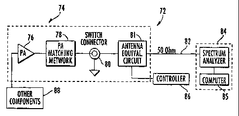
The system 72 in accordance with a non-limiting example as shown in FIG. 3,
includes a mobile wireless communications device 74 as a device-under-test in
which its
power amplifier 76 connects to its power amplifier matching network 78 and its
switch
connector 80. These components are similar to the components in FIG. 1. The
antenna
equivalent circuit 81 is connected by a connection line 82 to the monitoring
device, in this
CA 02638057 2008-07-17
non-limiting example, a spectrum analyzer 84. A separate computer 85 for
calculating
TRP can be connected to the spectrum analyzer, or the spectrum analyzer and
computer
could be integrated as one unit as shown by the dashed lines. The connection
line
corresponds to a cable having the impedance of the monitoring device as
measuring
equipment, in this case the spectrum analyzer 84. The connection line 82, in
one non-
limiting example, is a standard 50 ohm coaxial antenna cable used by many
skilled in the
art. The standard impedance based on monitoring devices is about 50 ohms, but
of course,
other lines as cables having different impedances could be used as long as
impedance
adjustments are made. The antenna equivalent circuit 81 and the overall system
72 are
designed under the assumption that the normal TRP measurement is lossless and
the RF
path loss can be calibrated out.
The simplified antenna equivalent circuit 81 can be used with a communications
test set for a spectrum analyzer 84, such as a Universal Radio Communication
Tester
CMU200, as manufactured by Rohde and Schwarz. To achieve accurate TRP
measurement through the antenna equivalent circuit 81, the input impedance of
this
circuit, for example, with a 50 ohm loading from the spectrum analyzer 84 to
its output
port, is designed to reflect the same impedance at a specified frequency point
as that of an
antenna of the portable wireless communications device. Thus, the antenna
equivalent
circuit operates similar to a lossless two-port network, for example, designed
using an RF
circuit design tool based on measured antenna input impedance. The antenna
equivalent
circuit 81 can vary in its impedance to match different frequencies, for
example, controlled
through a controller 86, which could include feedback from the device 74 or
spectrum
analyzer 84 or control the impedance based on programmed changes in transmit
frequencies from the device 74. As a result, the antenna equivalent circuit 81
can vary in
its impedance and look to the device 74 as if it is an antenna impedance at a
selected
single frequency point. The section of the device shown by dashed lines in
FIG. 3 could
be a separate module and connected to other components 88 and a mobile
wireless
communications device as a device-under-test as a non-limiting example.
FIG. 4 is an example of the antenna equivalent circuit 81 designed in a tuner
configuration such that the impedance can be changed to adapt to any frequency
for
testing. For this reason, the circuit can be termed an adaptive antenna
equivalent circuit.
This circuit includes a circuit line 90 of predetermined "n" wavelength and
two parallel,
variable capacitors 92 in a pie configuration and controlled by the controller
86 to operate
6
CA 02638057 2008-07-17
as a tuner for varying capacitance and thus impedance. In this example, a 1/8
wavelength
circuit line could be used, but other lengths based on different wavelengths
could be used
depending on the device-under-test, the transmit frequencies and other
variables. In this
example, capacitance can be varied to control the impedance, which changes
with transmit
frequency. As the frequency changes up and down, the impedance changes, and
thus, the
adaptive antenna equivalent circuit 81 as a tuner can vary to ensure any
proper impedance
match with the measuring equipment as a spectrum analyzer in this non-limiting
example.
Thus, the antenna equivalent circuit 81 is variable for the different
frequencies emitted by
the mobile wireless communications device. The controller 86 operates to
change the
capacitance of the tuner through the variable capacitors and controls the
proper impedance
as the mobile wireless communications device transmits or emits its RF energy
and
changes frequency during a test phase.
The Universal Radio Communication Tester in this example as the CMU200 is
only one non-limiting example of the type of measuring equipment as a
monitoring
device, for example, spectrum analyzer, which can be used, in accordance with
a non-
limiting example of the present invention. The equipment is a multi-protocol
tester for
current and future mobile radio networks that incorporates digital signal
processor (DSP)
technology, parallel measurements and remote command processing. It has a
modular
architecture that works similar to an oscilloscope probe with the DSP
dedicated to specific
local data acquisition and evaluation workload. Measurements can be made in a
signaling
and non-signaling mode and operated in remote or manual configuration. A
graphical user
interface simplifies operation. The system has a software platform and can
incorporate a
test stand as a fixture for holding a portable wireless communications device.
It is
possible to perform parallel testing of multiple mobile wireless
communications devices.
Further details are set forth in the CMU200 specification sheet.
In accordance with a non-limiting example of the present invention, total
radiated
power measurements can now be accomplished in 20 minutes using the system 72
as
described, as compared to multiple hours of testing in an anechoic chamber.
The mobile
wireless communications device does not have to be transported from a
development lab
to an anechoic chamber as in the prior art system shown in FIG. 1. The control
over the
antenna equivalent circuit as a tuner, as shown in FIG. 4, permits the system
to vary
impedance frequency changes during testing of the mobile wireless
communications
device.
7
CA 02638057 2008-07-17
FIG. 5 is a table showing a comparison made between normal TRP measurements
and an equivalent circuit measurement in accordance with a non-limiting
example of the
present invention. Measurements are shown for 850, 900, 1800 and 1900 MHz.
Frequencies are shown in the respective low, middle and high channels as
illustrated. Path
loss for a one-meter cable with 30 decibel attenuator is shown. The magnitude
phase in
degrees and the equivalent TRP measurement is illustrated. The TRP measurement
for
each of the four frequency bands with the three channels is shown.
A brief description will now proceed relative to FIGS. 6-8, which disclose an
example of a mobile wireless communications device, for example, a handheld
portable
cellular radio, which can incorporate the non-limiting examples of the various
circuits.
FIGS. 6-8 are representative non-limiting examples of the many different types
of
functional circuit components and their interconnection.
Referring initially to FIGS. 6 and 7, an example of a mobile wireless
communications device 120, such as a handheld portable cellular radio is first
described.
This device 120 illustratively includes a housing 121 having an upper portion
146 and a
lower portion 147, and a dielectric substrate (i.e., circuit board) 167, such
as a
conventional printed circuit board (PCB) substrate, for example, carried by
the housing. A
housing cover (not shown in detail) would typically cover the front portion of
the housing.
The term circuit board 167 as used hereinafter can refer to any dielectric
substrate, PCB,
ceramic substrate or other circuit carrying structure for carrying signal
circuits and
electronic components within the mobile wireless communications device 120.
The
illustrated housing 121 is a static housing, for example, as opposed to a flip
or sliding
housing which are used in many cellular telephones. However, these and other
housing
configurations may also be used.
Circuitry 148 is carried by the circuit board 167, such as a microprocessor,
memory, one or more wireless transceivers (e.g., cellular, WLAN, etc.), which
includes
RF circuitry, including audio and power circuitry, including any keyboard
circuitry. It
should be understood that keyboard circuitry could be on a separate keyboard,
etc., as will
be appreciated by those skilled in the art. A battery (not shown) is also
preferably carried
by the housing 121 for supplying power to the circuitry 148. The term RF
circuitry could
encompass the interoperable RF transceiver circuitry, power circuitry and
audio circuitry.
Furthermore, an audio output transducer 149 (e.g., a speaker) is carried by an
upper
portion 146 of the housing 121 and connected to the circuitry 148. One or more
user input
8
CA 02638057 2008-07-17
interface devices, such as a keypad (keyboard) 123 (FIG. 7), is also
preferably carried by
the housing 121 and connected to the circuitry 148. The term keypad as used
herein also
refers to the term keyboard, indicating the user input devices having lettered
and/or
numbered keys coniunonly known and other embodiments, including multi-top or
predictive entry modes. Other examples of user input interface devices include
a scroll
wheel 137 and a back button 136. Of course, it will be appreciated that other
user input
interface devices (e.g., a stylus or touch screen interface) may be used in
other
embodiments.
An antenna 145 is preferably positioned at the lower portion 147 in the
housing
and can be formed as a pattern of conductive traces that make an antenna
circuit, which
physically forms the antenna. It is connected to the circuitry 148 on the main
circuit board
167. In one non-limiting example, the antenna could be formed on an antenna
circuit
board section that extends from the circuit board at the lower portion of the
housing. By
placing the antenna 145 adjacent the lower portion 147 of the housing 121, the
distance is
advantageously increased between the antenna and the user's head when the
phone is in
use to aid in complying with applicable SAR requirements. Also, a separate
keyboard
circuit board could be used.
More particularly, a user will typically hold the upper portion of the housing
121
very close to his head so that the audio output transducer 149 is directly
next to his ear.
Yet, the lower portion 147 of the housing 121 where an audio input transducer
(i.e.,
microphone) is located need not be placed directly next to a user's mouth, and
can be held
away from the user's mouth. That is, holding the audio input transducer close
to the user's
mouth may not only be uncomfortable for the user, but it may also distort the
user's voice
in some circumstances. In addition, the placement of the antenna 145 adjacent
the lower
portion 147 of the housing 121 also advantageously spaces the antenna farther
away from
the user's brain.
Another important benefit of placing the antenna 145 adjacent the lower
portion
147 of the housing 121 is that this may allow for less impact on antenna
performance due
to blockage by a user's hand. That is, users typically hold cellular phones
toward the
middle to upper portion of the phone housing, and are therefore more likely to
put their
hands over such an antenna than they are an antenna mounted adjacent the lower
portion
147 of the housing 121. Accordingly, more reliable performance may be achieved
from
placing the antenna 145 adjacent the lower portion 147 of the housing 121.
9
CA 02638057 2008-07-17
Still another benefit of this configuration is that it provides more room for
one or
more auxiliary input/output (UO) devices 150 to be carried at the upper
portion 146 of the
housing. Furthermore, by separating the antenna 145 from the auxiliary UO
device(s) 150,
this may allow for reduced interference therebetween.
Some examples of auxiliary I/O devices 150 include a WLAN (e.g., Bluetooth,
IEEE 802.11) antenna for providing WLAN communication capabilities, and/or a
satellite
positioning system (e.g., GPS, Galileo, etc.) antenna for providing position
location
capabilities, as will be appreciated by those skilled in the art. Other
examples of auxiliary
I/O devices 150 include a second audio output transducer (e.g., a speaker for
speaker
phone operation), and a camera lens for providing digital camera capabilities,
an electrical
device connector (e.g., USB, headphone, secure digital (SD) or memory card,
etc.).
It should be noted that the term "input/output" as used herein for the
auxiliary I/O
device(s) 150 means that such devices may have input and/or output
capabilities, and they
need not provide both in all embodiments. That is, devices such as camera
lenses may
only receive an optical input, for example, while a headphone jack may only
provide an
audio output.
The device 120 further illustratively includes a display 122, for example, a
liquid
crystal display (LCD) carried by the housing 121 and connected to the
circuitry 148. A
back button 136 and scroll wheel 137 can also be connected to the circuitry
148 for
allowing a user to navigate menus, text, etc., as will be appreciated by those
skilled in the
art. The scroll wheel 137 may also be referred to as a "thumb wheel" or a
"track wheel" in
some instances. The keypad 123 illustratively includes a plurality of multi-
symbol keys
124 each having indicia of a plurality of respective symbols thereon. The
keypad 123 also
illustratively includes an alternate function key 125, a next key 126, a space
key 127, a
shift key 128, a return (or enter) key 129, and a backspace/delete key 130.
The next key 126 is also used to enter a"*" symbol upon first pressing or
actuating
the alternate function key 125. Similarly, the space key 127, shift key 128
and backspace
key 130 are used to enter a "0" and "#", respectively, upon first actuating
the alternate
function key 125. The keypad 123 further illustratively includes a send key
131, an end
key 132, and a convenience (i.e., menu) key 139 for use in placing cellular
telephone calls,
as will be appreciated by those skilled in the art.
Moreover, the symbols on each key 124 are arranged in top and bottom rows. The
symbols in the bottom rows are entered when a user presses a key 124 without
first
CA 02638057 2008-07-17
pressing the alternate function key 25, while the top row symbols are entered
by first
pressing the alternate function key. As seen in FIG. 7, the multi-symbol keys
124 are
arranged in the first three rows on the keypad 123 below the send and end keys
131, 132.
Furthermore, the letter symbols on each of the keys 124 are arranged to define
a
QWERTY layout. That is, the letters on the keypad 123 are presented in a three-
row
format, with the letters of each row being in the same order and relative
position as in a
standard QWERTY keypad.
Each row of keys (including the fourth row of function keys 125-129) is
arranged
in five columns. The multi-symbol keys 124 in the second, third, and fourth
colunms of
the first, second, and third rows have numeric indicia thereon (i.e., I
through 9) accessible
by first actuating the alternate function key 125. Coupled with the next,
space, and shift
keys 126, 127, 128, which respectively enter a"*", "0", and "#" upon first
actuating the
alternate function key 125, as noted above, this set of keys defines a
standard telephone
keypad layout, as would be found on a traditional touch-tone telephone, as
will be
appreciated by those skilled in the art.
Accordingly, the mobile wireless communications device 120 as described may
advantageously be used not only as a traditional cellular phone, but it may
also be
conveniently used for sending and/or receiving data over a cellular or other
network, such
as Internet and email data, for example. Of course, other keypad
configurations may also
be used in other embodiments. Multi-tap or predictive entry modes may be used
for
typing e-mails, etc. as will be appreciated by those skilled in the art.
The antenna 145 is preferably formed as a multi-frequency band antenna, which
provides enhanced transmission and reception characteristics over multiple
operating
frequencies. More particularly, the antenna 145 is designed to provide high
gain, desired
impedance matching, and meet applicable SAR requirements over a relatively
wide
bandwidth and multiple cellular frequency bands. By way of example, the
antenna 145
preferably operates over five bands, namely a 850 MHz Global System for Mobile
Communications (GSM) band, a 900 MHz GSM band, a DCS band, a PCS band, and a
WCDMA band (i.e., up to about 2100 MHz), although it may be used for other
bands/frequencies as well. To conserve space, the antenna 145 may
advantageously be
implemented in three dimensions although it may be implemented in two-
dimensional or
planar embodiments as well.
11
CA 02638057 2008-07-17
The mobile wireless communications device shown in FIGS. 6 and 7 can
incorporate e-mail and messaging accounts and provide different functions such
as
composing e-mail, PIN messages, and SMS messages. The device can manage
messages
through an appropriate menu that can be retrieved by choosing a messages icon.
An
address book function could add contacts, allow management of an address book,
set
address book options and manage SIM card phone books. A phone menu could allow
for
the making and answering of phone calls using different phone features,
managing phone
call logs, setting phone options, and viewing phone information. A browser
application
could permit the browsing of web pages, configuring a browser, adding
bookmarks, and
changing browser options. Other applications could include a task, memo pad,
calculator,
alarm and games, as well as handheld options with various references.
A calendar icon can be chosen for entering a calendar program that can be used
for
establishing and managing events such as meetings or appointments. The
calendar
program could be any type of messaging or appointment/meeting program that
allows an
organizer to establish an event, for example, an appointment or meeting.
A non-limiting example of various functional components that can be used in
the
exemplary mobile wireless communications device 120 of FIGS. 6 and 7 is
further
described in the example below with reference to FIG. 8. The device 120
illustratively
includes a housing 220, a keypad 240 and an output device 260. The output
device 260
shown is preferably a display, which is preferably a full graphic LCD. Other
types of
output devices may alternatively be used. A processing device 280 is contained
within the
housing 220 and is coupled between the keypad 240 and the display 260. The
processing
device 280 controls the operation of the display 260, as well as the overall
operation of the
mobile device 120, in response to actuation of keys on the keypad 240 by the
user.
The housing 220 may be elongated vertically, or may take on other sizes and
shapes (including clamshell housing structures). The keypad may include a mode
selection
key, or other hardware or software for switching between text entry and
telephony entry.
In addition to the processing device 280, other parts of the mobile device 120
are
shown schematically in FIG. 8. These include a communications subsystem 201; a
short-
range communications subsystem 202; the keypad 240 and the display 260, along
with
other input/output devices 206, 208, 210 and 212; as well as memory devices
216, 218 and
various other device subsystems 221. The mobile device 120 is preferably a two-
way RF
communications device having voice and data communications capabilities. In
addition,
12
CA 02638057 2008-07-17
the mobile device 120 preferably has the capability to communicate with other
computer
systems via the Internet.
Operating system software executed by the processing device 280 is preferably
stored in a persistent store, such as the flash memory 216, but may be stored
in other types
of memory devices, such as a read only memory (ROM) or similar storage
element. In
addition, system software, specific device applications, or parts thereof, may
be
temporarily loaded into a volatile store, such as the random access memory
(RAM) 218.
Communications signals received by the mobile device may also be stored in the
RAM
218.
The processing device 280, in addition to its operating system functions,
enables
execution of software applications 230A-230N on the device 120. A
predetermined set of
applications that control basic device operations, such as data and voice
communications
230A and 230B, may be installed on the device 120 during manufacture. In
addition, a
personal information manager (PIM) application may be installed during
manufacture.
The PIM is preferably capable of organizing and managing data items, such as e-
mail,
calendar events, voice mails, appointments, and task items. The PIM
application is also
preferably capable of sending and receiving data items via a wireless network
241.
Preferably, the PIM data items are seamlessly integrated, synchronized and
updated via
the wireless network 241 with the device user's corresponding data items
stored or
associated with a host computer system.
Communication functions, including data and voice communications, are
performed through the communications subsystem 201, and possibly through the
short-
range communications subsystem. The communications subsystem 201 includes a
receiver
250, a transmitter 252, and one or more antennae 254 and 256. In addition, the
communications subsystem 201 also includes a processing module, such as a
digital signal
processor (DSP) 258, and local oscillators (LOs) 261. The specific design and
implementation of the communications subsystem 201 is dependent upon the
communications network in which the mobile device 120 is intended to operate.
For
example, the mobile device 120 may include a communications subsystem 101
designed
to operate with the MobitexTM, Data TACTM or General Packet Radio Service
(GPRS)
mobile data communications networks, and also designed to operate with any of
a variety
of voice communications networks, such as AMPS, TDMA, CDMA, PCS, GSM, etc.
13
CA 02638057 2008-07-17
Other types of data and voice networks, both separate and integrated, may also
be utilized
with the mobile device 120.
Network access requirements vary depending upon the type of communication
system. For example, in the Mobitex and DataTAC networks, mobile devices are
registered on the network using a unique personal identification number or PIN
associated
with each device. In GPRS networks, however, network access is associated with
a
subscriber or user of a device. A GPRS device therefore requires a subscriber
identity
module, commonly referred to as a SIM card, in order to operate on a GPRS
network.
When required network registration or activation procedures have been
completed,
the mobile device 120 may send and receive communications signals over the
communication network 241. Signals received from the communications network
241 by
the antenna 254 are routed to the receiver 250, which provides for signal
amplification,
frequency down conversion, filtering, channel selection, etc., and may also
provide analog
to digital conversion. Analog-to-digital conversion of the received signal
allows the DSP
258 to perform more complex communications functions, such as demodulation and
decoding. In a similar manner, signals to be transmitted to the network 241
are processed
(e.g., modulated and encoded) by the DSP 258 and are then provided to the
transmitter
252 for digital to analog conversion, frequency up conversion, filtering,
amplification and
transmission to the communication network 241 (or networks) via the antenna
256.
In addition to processing communications signals, the DSP 258 provides for
control of the receiver 250 and the transmitter 252. For example, gains
applied to
communications signals in the receiver 250 and transmitter 252 may be
adaptively
controlled through automatic gain control algorithms implemented in the DSP
258.
In a data communications mode, a received signal, such as a text message or
web
page download, is processed by the communications subsystem 201 and is input
to the
processing device 280. The received signal is then further processed by the
processing
device 280 for an output to the display 260, or alternatively to some other
auxiliary I/O
device 206. A device user may also compose data items, such as e-mail
messages, using
the keypad 240 and/or some other auxiliary I/O device 206, such as a touchpad,
a rocker
switch, a thumb-wheel, or some other type of input device. The composed data
items may
then be transmitted over the communications network 241 via the communications
subsystem 201.
14
CA 02638057 2008-07-17
In a voice communications mode, overall operation of the device is
substantially
similar to the data communications mode, except that received signals are
output to a
speaker 210, and signals for transmission are generated by a microphone 212.
Alternative
voice or audio UO subsystems, such as a voice message recording subsystem, may
also be
implemented on the device 120. In addition, the display 260 may also be
utilized in voice
communications mode, for example to display the identity of a calling party,
the duration
of a voice call, or other voice call related information.
Any short-range communications subsystem enables communication between the
mobile device 120 and other proximate systems or devices, which need not
necessarily be
similar devices. For example, the short-range communications subsystem may
include an
infrared device and associated circuits and components, or a BluetoothTM
communications
module to provide for communication with similarly-enabled systems and
devices.
Many modifications and other embodiments of the invention will come to the
mind
of one skilled in the art having the benefit of the teachings presented in the
foregoing
descriptions and the associated drawings. Therefore, it is understood that the
invention is
not to be limited to the specific embodiments disclosed, and that
modifications and
embodiments are intended to be included within the scope of the appended
claims.