Note: Descriptions are shown in the official language in which they were submitted.
CA 02638531 2008-08-07
,.4 w
ELECTRIC POWER STEERING APPARATUS
BACKGROUND OF THE INVENTION
[0001]
The present invention relates to an electric power steering apparatus.
[0002]
FIG. 4 is a block diagram of an electric power steering apparatus 100
described in Japanese Patent No. 3154665. In the drawing, controller 101
controls a steering auxiliary motor M based on a vehicle speed output from a
vehicle speed sensor and a steering torque output from a torque sensor.
[0003]
In the drawing, reference numeral 102 denotes an H bridge circuit. The
H bridge circuit 102 is driven by an FET driving circuit 103. The FET driving
circuit 103 is subjected to PWM (pulse-width modulation) control by the
controller 101 based on a PWM signal.
[0004]
The controller 101 obtains a difference between a current command
value associated with the vehicle speed and the steering torque, and a current
actually flowing through the steering auxiliary motor M. The controller then
performs PWM control with respect to the FET driving circuit 103 based on
this difference.
[0005]
The current actually flowing through the steering auxiliary motor M is
obtained by detecting a voltage across a motor current detection resistance
104.
[0006]
-1-
CA 02638531 2008-08-07
The voltage across the motor current detection resistance 104 is
supplied to a sample-hold circuit 105 and held as a voltage across a capacitor
Cl in the sample-hold circuit 105.
[0007]
The voltage held in the capacitor Cl is input to an operational amplifier
106 as a voltage across the input terminals of the operational amplifier 106.
The voltage is amplified in the operational amplifier 106.
[0008]
An output from the operational amplifier 106 is supplied to a base of a
PNP transistor Q 10 to turn the transistor Q 10 on, which causes a collector
current to flow. The collector current flows through a collector resistance
R14
and is converted into a voltage, which is read into the controller 101. Since
the
collector current in the PNP transistor Q10 is associated with a magnitude of
the voltage across the motor current detection resistance 104, the controller
101 can obtain a magnitude of the current actually flowing through the
steering auxiliary motor M based on the magnitude of the collector current.
[0009]
However, this conventional electric power steering apparatus 100 has
the following disadvantage. Since the operational amplifier 106 generally has
an offset voltage, when a current flowing through the motor current detection
resistance 104 is small, the current cannot be detected because of the
influence
of the offset voltage. Therefore, there is a problem in that accurate assist
control cannot be executed by the electric power steering apparatus 100.
[0010]
Japanese Published Patent Application No. 1992-251596 discloses
another electric power steering apparatus, in which an influence of an offset
-2-
CA 02638531 2008-08-07
voltage is eliminated. FIG. 5 illustrates the device described in that
document.
A voltage across a shunt resistance Rs is detected by a differential circuit
51. A
predetermined voltage Vr is applied to a positive input terminal of the
differential circuit 51. The voltage detected by the differential circuit 51
is
supplied to a negative input terminal of a comparator 53. The comparator 53
executes half-wave rectification. A connection point between the shunt
resistance Rs and a battery 48 is connected to a positive input terminal of a
differential circuit 52. The predetermined voltage Vr is also applied to the
positive input terminal of this differential circuit 52. The differential
circuit 52
compensates for an offset voltage generated by the differential circuit 51 and
the comparator 53.
[0011]
However, in the device described in Japanese Published Patent
Application No. 1992-251596, which is thus configured to compensate for the
offset voltage, there is a problem in that the circuit configuration is
complicated and selection of its respective elements is troublesome. A device
that can easily and accurately execute assist control by enabling compensation
for the offset voltage but with a simple structure has thus been demanded.
[0012]
Another known electric power steering apparatus is described in
Japanese Published Patent Application No. 2002-46630.
[0013]
In the electric power steering apparatus disclosed in that document, a
current value flowing through a motor current detection resistance is held in
a
peak hold circuit and then fetched into a controller.
[0014]
-3-
CA 02638531 2008-08-07
FIG. 6 shows the peak hold circuit 60 described in Japanese Published
Patent Application No. 2002-46630. This peak hold circuit 60 includes a first
peak hold circuit 61 and a second peak hold circuit 62. Operation of the first
peak hold circuit 61 will now be explained. When a motor current flows
through a motor current detection resistance 56, a potential at a non-
inverting
input terminal of a comparator 61a (a potential at a point U) is increased.
When this potential at the non-inverting input terminal of the comparator 61a
is higher than a potential at an inverting input terminal of the comparator
61a,
the comparator 61a is turned off and a diode 61c is turned on. As a result, a
current flows through a capacitor 61f via a resistance 61g and the diode 61c,
and the capacitor 61f is charged. Based on this charge, when the potential at
the non-inverting input terminal of the comparator 61a becomes higher than
the potential at the non-inverting input terminal of the comparator 61a, the
comparator 61a is turned on, the diode 61c is turned off, charging of the
capacitor 61f is stopped, and discharging of the capacitor 61f is carried out
via
resistances 61d and 61e. An operational amplifier 61b converts a potential
VP 1 at a point P 1 into a low impedance and outputs this impedance to a
channel CHI of an ADC 43. Respective values of elements in the first peak
hold circuit 61, e.g., resistance values R1 and R2 or a capacitance of the
capacitor 61f are selected in such a manner that a maximum value of an
analog voltage VP1 (the analog voltage VP1 when a motor current has a
maximum value that can be taken under control) becomes equal to a
maximum value of a voltage that can be subjected to analog/digital conversion
by the ADC 43.
[0015]
-4-
CA 02638531 2008-08-07
However, the invention described in Japanese Published Patent
Application No. 2002-46630 has the following problem. FIG. 7(a) shows a
waveform of a PWM signal. FIG. 7(b) depicts a voltage generated in the motor
current detection resistance 56. Furthermore, as shown in FIG.7(b), a time
constant that is determined based on the capacitance of the capacitor 61f and
the resistance values Rl and R2 of the resistances 61d and 61e is set with
respect to the capacitor 61f so that the same voltage as the voltage generated
in the motor current detection resistance 56 can be produced. However, when
the time constant is too large, discharge of the voltage in the capacitor 61f
takes a long time, and a voltage generated in the motor current detection
resistance 56 in synchronization with the next PWM signal is thereby added
before the voltage in the capacitor 61f is completely discharged. Therefore,
the
voltage in the capacitor 61f becomes a voltage higher than the voltage
currently generated in the current detection resistance 56, thus leading to a
problem in that the motor current cannot be accurately detected.
[0016]
When the time constant is too small, the capacitor 61f cannot hold the
voltage for a fixed time and can readily discharge the voltage. As a result,
the
voltage in the capacitor 61f is discharged before the controller reliably
fetches
the voltage in the capacitor 61f, thereby leading to a problem in that the
controller cannot execute accurate assist control.
[0017]
That is, in the invention disclosed in Japanese Published Patent
Application No. 2002-46630, when performing accurate assist control, there
occurs a problem that adjustment of the time constant determined based on
-5-
CA 02638531 2008-08-07
the capacitor 61f and the resistance values R1 and R2 of the discharge
resistances 61d and 61e is complicated.
[0018]
Therefore, in view of the problems in the conventional technology, it is
an object of the present invention to provide an electric power steering
apparatus that has a simple structure and which enables highly accurate
detection of a current value actually flowing through a steering motor to
execute accurate assist control.
SUMMARY OF THE INVENTION
[0019]
The invention provides an electric power steering apparatus. A
preferred embodiment of the invention may include a vehicle speed sensor that
detects a vehicle speed, a torque sensor that detects a steering torque of a
steering device such as a steering wheel, a steering auxiliary motor for the
steering device, a motor current detector that detects a value of a motor
current actually flowing through the motor, and a controller that obtains a
difference between a current command value calculated based on the vehicle
speed and the steering torque and the value of the motor current actually
flowing through the motor to perform PWM control with respect to an
operation of the motor. A motor current hold section that holds the value of
the
motor current detected by the motor current detector may be included, with a
switching device being provided between the motor current detector and the
motor current hold section. The controller can sample the motor current value
detected by the motor current detector at a sampling start timing for turning
on the switching device to start holding in the motor current hold section,
and
-6-
CA 02638531 2008-08-07
fetching the motor current value held in the motor current hold section at a
hold timing for turning off the switching device. Finally, the sampling start
timing and the hold timing can be variable.
[0020]
The controller can change the sampling start timing and the hold
timing without restraint by controlling opening and closing of the switching
device in accordance with, e.g., a magnitude of a pulse width of the PWM
signal, thereby executing accurate assist control.
BRIEF DESCRIPTION OF THE DRAWINGS
[0021]
FIG. 1 is a block diagram of an example of an electric power steering
apparatus according to an embodiment of the invention;
FIGS. 2(A)-2(K) are views showing relationships between a PWM signal,
a motor current, a voltage across a motor current detection resistance, and a
sampling signal according to several distinct embodiments;
FIG. 3 is a diagram showing characteristics of an operational amplifier
used in the embodiment;
FIG. 4 is a block diagram of an electric power steering apparatus in a
conventional device;
FIG. 5 is a block diagram of an electric power steering apparatus in a
conventional technology;
FIG. 6 is a block diagram of an electric power steering apparatus in a
conventional device;
-7-
CA 02638531 2008-08-07
FIG. 7a is a view showing a waveform of a PWM signal; and
FIG. 7b is a view showing a waveform of a voltage generated in a motor
current detection resistance in a conventional electric power steering
apparatus.
DETAILED DESCRIPTION OF PREFERRED EMBODIMENTS
[0022]
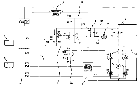
FIGS. I to 3 depict embodiments of the present invention. In FIG. 1,
reference numeral 1 denotes a motor circuit. The motor circuit 1 is formed by
bridge-connecting four switching elements Si to S4. Each of these switching
elements includes, e.g., an FET. The motor circuit 1 includes two of the
switching elements Sl and S2 on a high side, the other two switching elements
S3 and S4 on a low side, and a steering auxiliary motor M between the two
switching elements SI and S2 on the high side and the two switching elements
S3 and S4 on the low side.
[0023]
The motor circuit 1 is connected to a motor power supply 2 through a
motor current detection resistance R6. The motor current detection resistance
R6 includes a motor current detector.
[0024]
The four switching elements Sl to S4 in the motor circuit 1 are
connected to a boosting power supply S to receive power, and controlled by a
motor circuit driving section 3. The motor circuit driving section 3 is
controlled
by controller 4 to perform PWM control with respect to the switching elements
in the motor circuit 1 based on a PWM signal. The controller 4 comprises,
e.g.,
-8-
CA 02638531 2008-08-07
a microcomputer. Additionally, the switching elements S1 and S4, and S2 and
S3 in diagonal directions form respective pairs. Further, the boosting power
supply S is connected with the motor power supply 2 to boost a voltage in the
motor power supply 2.
[0025]
The controller 4 calculates a current command value based on a vehicle
speed output from a vehicle speed sensor 5 and a steering torque output from
a torque sensor 6. The controller obtains a difference between the current
command value and a current value actually flowing through the steering
auxiliary motor M and performs PWM control with respect to the motor circuit
1 based on this difference.
[0026]
A motor current hold section 7 and a motor current output section 8 are
provided between the motor current detection resistance R6 and the controller
4. A value of the motor current detection resistance R6 is fetched into the
controller 4 through the motor current hold section 7 and the motor current
output section 8.
[00271
A switching device 9 is provided between the motor current detection
resistance R6 and the motor current hold section 7. The switching device 9 is
controlled to switch on and off by a switching controller 10.
[0028]
The motor current hold section 7 includes a capacitor C1 and a
discharge resistance R4 connected in parallel to the motor current detection
resistance R6. A first reference line X1 and a second reference line X2 are
provided at respective ends of the motor current detection resistance R6. The
-9-
CA 02638531 2008-08-07
capacitor Cl and the discharge resistance R4 are provided between the first
reference line X1 and the second reference line X2. The first reference line
X1
is connected to a positive side of the motor power supply 2 and thus has a
fixed
potential.
[0029]
The motor current output section 8 includes an operational amplifier 11
and a transistor Q5 at the rear of the operational amplifier 11. A negative
terminal of the operational amplifier 11 is connected to the first reference
line
Xl, with a positive terminal of the operational amplifier connected to a
second
reference line X2. An output from the operational amplifier 11 is connected to
a base of the transistor Q5 through a resistance R7. An emitter resistance R8
is connected to an emitter side of the transistor Q5, and a collector side of
the
transistor Q5 is connected to the first reference line Xl.
[0030]
A current flowing through the emitter side of the transistor Q5 is
converted into a voltage by the emitter resistance R8 and input to an AD
terminal of the controller 4 through a resistance R9 and a capacitor C4.
[0031]
An offset circuit 12 is connected to the first reference line Xl. The offset
circuit 12 includes the boosting power supply S, a first resistance Rl with a
negative side connected to a positive side of the boosting power supply S, a
zener diode ZD with a cathode side connected to the other side of the first
resistance Rl and an anode side connected to a positive side of the motor
power supply 2, and a second resistance R2 between the cathode side of the
zener diode ZD and the first reference line X1.
[0032]
-10-
CA 02638531 2008-08-07
The switching device 9 is provided on the second reference line X2. The
switching device 9 can be, e.g., a MOSFET of an N channel. If the switching
device 9 is formed of the N-channel MOSFET, the switching device 9 is turned
on when a high voltage is applied to a gate side of the switching device 9,
and
turned off when a low voltage is applied to the gate of the switching device
9.
[0033]
The switching control section 10 can include a grounded-emitter NPN
transistor. A base side of this transistor is connected with a terminal P00 of
the controller 4 through a resistance Rll and grounded through a resistance
R12. A collector side of this transistor is connected at a positive side of
the
boosting power supply S through a resistance R10 and also connected to a gate
side of the MOSFET that constitutes the switching device 9. A sampling signal
P is output from the controller 4 to a base side of the switching control
section
10.
[0034]
The electric power steering apparatus according to this embodiment
performs PWM control with respect to the switching elements S1 and S2 alone.
As the controller 4 turns the switching elements S1 and S2 in the motor
circuit
1 on and off, the steering auxiliary motor M is subjected to PWM control based
on a PWM signal. When the switching element Sl is turned on, for example,
as shown in FIG. 1, a current K flows through the motor circuit 1. When the
current K flows through the motor circuit 1 in this manner, a motor current
flows through the motor current detection resistance 6, and a voltage V1 is
produced between the first reference line X1 and the second reference line X2.
[0035]
-11-
CA 02638531 2008-08-07
On the other hand, when the switching element S1 is turned off, since
the current does not flow through the motor current detection resistance R6,
the voltage is not produced between the first reference line Xl and the second
reference line X2. In this case, a regenerative current produced in the
steering
auxiliary motor M circulates in a path extending from the steering auxiliary
motor M and returning to the steering auxiliary motor M via the diodes of the
switching element S4 and the switching element S3, and is then annihilated.
[00361
When the switching element S2 is turned on, the current flows through
the motor circuit 1, the motor current flows through the motor current
detection resistance 6, and the voltage Vl is produced between the first
reference line X1 and the second reference line X2. When the switching
element S2 is turned off, since the current does not flow through the motor
current detection resistance R6, the voltage is not produced between the first
reference line Xl and the second reference line X2. In this case, the
regenerative current produced in the steering auxiliary motor M circulates in
a path extending from the steering auxiliary motor M and returning to the
steering auxiliary motor M via the diodes of the switching element S3 and the
switching element S4, and is then annihilated.
[0037]
When the sampling signal P is supplied from the controller 4 to the
switching control section 10 in synchronization with the switching elements
S1 or S2 being turned on and the switching control section 10 is thereby
turned on, a high voltage is applied to an FET of the switching device 9 to
turn
the switching device on. As a result, a voltage across the capacitor Cl
becomes
-12-
CA 02638531 2008-08-07
the voltage V1 between the first reference line Xl and the second reference
line X2.
[0038]
The voltage Vi of the capacitor Cl is applied to a part of the circuit
between the input terminals of the operational amplifier 11. In this case, a
current flows in such a manner that an imaginary short-circuit occurs in the
operational amplifier 11. This current flows through the collector side of the
transistor Q5 as indicated by an arrow in FIG. 1 to become an emitter current,
and a voltage V2 is generated in the emitter resistance R8.
[0039]
This voltage V2 is read into the controller 4 from the terminal AD of the
controller 4. This voltage V2 is associated with the voltage V1 at both ends
of
the motor current detection resistance R6. Detecting an increase or decrease
in this voltage V2 enables the detection of an increase or decrease of the
voltage Vl.
[0040]
A voltage of the capacitor C1 can be read by the controller 4 with
appropriate timing.
[0041]
First, based on FIGS. 2(A)-2(K), descriptions will be given of
relationships between a triangular wave (shown in FIG. 2(A)) that is a basis
for shaping of a pulse wave of the PWM signal used for PWM control, timings
of rising and falling of the PWM signal (shown in FIG. 2(B)), a waveform of
the
motor current (shown in FIG. 2(C)), the voltage at both ends of the motor
current detection resistance (shown in FIG. 2(D)), and the sampling signal P
(shown in FIGS. 2(E) to (K)).
-13-
CA 02638531 2008-08-07
[0042]
The pulse wave of the PWM signal used for the PWM control (shown in
FIG. 2(B)) can be formed by using, e.g., a limiter circuit having a variable
threshold value, The pulse wave can be shaped into a rectangular wave by
passing the triangular wave depicted in FIG. 2(A) to, e.g., the limiter
circuit.
FIG. 2(B) shows the PWM signal shaped into a rectangular wave with a fixed
pulse width by passing the triangular wave to the limiter circuit having a
threshold value T1.
[0043]
The sampling signal P is a signal that is supplied from the controller 4
to the switching control section 10 and which turns the switching device 9 on
and off. A pulse width of the sampling signal P is called a sampling time AT.
Although the sampling signal P essentially has a negative voltage, it will be
explained as having a positive voltage for the sake of convenience.
[0044]
When the switching control section 10 is activated to turn on the
switching device 9 based on a rise of the sampling signal P, sampling of the
voltage in the motor current detection resistance R6 begins. Rising of the
sampling signal P corresponds to a sampling start timing. When the switching
device 9 is turned off based on a fall of the sampling signal P, sampling is
stopped. The controller 4 fetches the voltage V1 in the capacitor Cl in
synchronization with falling of the sampling signal P. A time of falling of
the
sampling signal P corresponds to a hold time H.
[0045]
The controller 4 can change the sampling start timing S and the hold
timing H.
-14-
CA 02638531 2008-08-07
[0046]
Since the sampling start timing S and the hold timing H can be changed,
the following effect can be achieved. In the invention disclosed in Japanese
Published Patent Application No. 2002-46630 and depicted in FIG. 6, the time
constant determined based on a capacitance of the capacitor and resistance
value of the discharge resistances must be highly accurately adjusted, and
this
adjustment is complicated. In the present embodiment, though, the controller
4 can change the sampling start timing S and the hold timing H without
restraint by controlling times at which the switching device 9 is turned on or
off. As a result, the controller 4 can start sampling of a motor current value
with optimum timing and can read the motor current value with optimum
timing, and thereby execute optimum assist control.
[0047]
Cases in which the sampling start timing S and the hold timing H are
changed in various embodiments will now be explained.
[0048]
FIG. 2(E) illustrates a first embodiment. This first embodiment
corresponds to a case in which the sampling time aT is fixed and the hold
timing H is synchronized with falling of the PWM signal. In this first
embodiment, since a time for subjecting a motor current value detected in the
motor current detection resistance R6 to AD conversion can be sufficiently
assured by providing enough sampling time AT, an analog value can be
converted into a digital value even if the AD converter requires a long
conversion time. Furthermore, sampling software can be simplified by fixing
the sampling time AT. Moreover, since the hold timing H is synchronized with
-15-
CA 02638531 2008-08-07
falling of the PWM signal, the hold timing H does not have to be
independently controlled, which facilitates its implementation.
[0049]
FIG. 2(F) shows a second embodiment. In this second embodiment, the
hold timing H can be set immediately before falling of the PWM signal. As to
the hold timing H in this case, a point N where a threshold value T2 which is
not smaller than the threshold value T1 crosses the triangular wave can be
determined as the hold timing H.
[0050]
FIG. 2(G) shows a third embodiment in which the sampling start timing
S can be synchronized with rising of the PWM signal, and the hold timing H
can be synchronized with falling of the PWM signal. When the sampling start
timing S is synchronized with rising of the PWM signal and the hold timing H
is synchronized with falling of the PWM signal, the sampling start timing S
and the hold timing H can be readily assured without preparing a dedicated
timer or program software.
[0051]
FIG. 2(H) shows a fourth embodiment in which the center of the
sampling time AT, i.e., the center of a pulse width of the sampling signal,
matches with the center of a pulse width of the PWM signal, and in which the
sampling time OT is fixed. In this case, as shown in FIG. 2(D), a substantial
average value of the voltage across the motor current detection resistance R6,
which is gradually increased when the PWM signal is ON, can be detected,
and a substantial average value of the motor current can thereby be detected,
thus executing assist control according to an actual state based on this
substantial average value. When the sampling time AT is set to a fixed time
-16-
CA 02638531 2008-08-07
that is not smaller than the time required for AD conversion, an AD converter
that requires a relatively long conversion time can be used. Furthermore,
when the sampling time AT is fixed, software required for sampling can be
simplified.
[0052]
FIG. 2(I) shows a fifth embodiment in which the sampling signal P is
output before a timing at the center of a pulse width of the PWM signal, and
the center of the pulse width of the PWM signal is determined as the hold
timing H. In this case, as shown in FIG. 2(D), the controller 4 can detect an
average value of the voltage across the motor current detection resistance R6,
which is gradually increased when the PWM signal is ON, and can thereby
detect an average value of the motor current, thus executing ideal assist
control according to an actual state based on this average value.
[0053]
A sixth embodiment will now be explained. In this sixth embodiment,
the sampling start timing S and the hold timing H can be changed in
accordance with a large current region and a small current region. In the
large
current region, as shown in FIG. 2(J), the sampling start timing S is provided
before the rise of the PWM signal, and the hold timing H is matched with the
center of the pulse width of the PWM signal. In the small current region, as
shown in FIG. 2(G), the sampling start timing S is synchronized the rise of
the
PWM signal, and the hold timing H is synchronized with falling of the PWM
signal.
[0054]
In the large current region, when the sampling start timing S is
provided before rising of the PWM signal and the hold timing H is
-17-
CA 02638531 2008-08-07
synchronized with the center of the pulse width of the PWM signal as shown
in FIG. 2(J), the controller 4 can detect an average value of the voltage
across
the motor current detection resistance R6, which is gradually increased when
the PWM signal is ON, and can thereby detect an average value of the motor
current as shown in FIG. 2(D), thus executing ideal assist control according
to
an actual state based on this average value. Moreover, when the sampling
start timing S is provided before rising of the PWM signal, the relatively
long
sampling time AT from the sampling start timing S to the hold timing H can
be assured, and hence an AD converter which requires a relatively long
processing time for AD conversion can be used.
[0055]
Additionally, in the small current region, when the sampling start
timing S is synchronized with rising of the PWM signal and the hold timing H
is synchronized with falling of the PWM signal as shown in FIG. 2(G), the
controller 4 can accurately synchronize the sampling start timing S with
rising
of the PWM signal and also synchronize the hold timing H with falling of the
PWM signal to precisely fetch the voltage Vl generated in the motor current
detection resistance R6 even in the small current region where the pulse width
of the PWM signal is narrowed, thus executing accurate assist control based
on the voltage V 1.
[0056]
A seventh embodiment will now be explained. In this seventh
embodiment, the sampling start timing S can be synchronized with rising of
the PWM signal and the hold timing H can be synchronized with falling of the
PWM signal in the large current region as shown in FIG. 2(G), whilst the
sampling start timing S is provided before rising of the PWM signal and the
-18-
CA 02638531 2008-08-07
hold timing H can be synchronized with falling of the PWM signal in the small
current region as shown in FIG. 2(K).
[0057]
In this case, in the large current region, when the sampling start timing
S and the hold timing H are synchronized with rising and falling of the PWM
signal, the sampling start timing S and the hold timing H can be readily
assured without preparing a dedicated timer or program software.
[0058]
Further, in the small current region, since sampling can be started
without falling behind rising of the PWM signal by providing the sampling
start timing S before rising of the PWM signal, sampling can be accurately
performed even if a duty ratio of the PWM signal is small. Furthermore, when
the hold timing H is synchronized with falling of the PWM signal, the hold
timing H can be easily assured without preparing a dedicated timer or
program soft. Providing the hold timing H in synchronization with the center
of the pulse width of the PWM signal is ideal in an implication that sampling
an average value of the motor current is most preferable, but a sampled value
does not have a large difference from an ideal value even if the hold timing H
is synchronized with falling of the PWM signal rather than the center of the
pulse width of the PWM signal since the pulse width of the PWM signal is
very narrow in the small current region.
[0059]
An eighth embodiment will now be explained. In this eighth
embodiment, as shown in FIG. 2(G), the sampling start timing S is
synchronized with rising of the PWM signal, the hold timing H is synchronized
with falling of the PWM signal in the large current region, and the sampling
-19-
CA 02638531 2008-08-07
time AT is fixed in the small current region in addition to the requirements
explained in connection with the seventh embodiment.
[0060]
In this eighth embodiment, in the large current region, when the
sampling start timing S and the hold timing H are synchronized with rising
and falling of the PWM signal, the sampling start timing S and the hold
timing H can be readily assured without preparing a dedicated timer or
program software.
[0061]
Further, in the small current region, since a time required to perform
AD conversion with respect to a motor current value detected by the motor
current detection resistance R6 can be sufficiently assured by providing
enough sampling time AT, in addition to the function and the effect in the
small current region explained in the seventh embodiment, an analog value
can be converted into a digital value even if an AD converter requiring a long
conversion time is used. Furthermore, software for sampling can be simplified
by fixing the sampling time AT.
[0062]
A function of the offset circuit 12 will now be explained. Although a
fixed potential is generated on the cathode side of the zener diode ZD when a
current supplied from the boosting power supply S passes through the first
resistance R1, the fixed potential is maintained by a zener effect of the
zener
diode ZD. Therefore, a fixed current associated with a voltage between the
potential on the cathode side of the zener diode ZD and the first reference
line
Xl flows through the second resistance R2. Moreover, when this current flows
through the emitter resistance R8 of the transistor Q5, a voltage based on the
-20-
CA 02638531 2008-08-07
current supplied from the boosting power supply S is constantly added to this
emitter resistance R8. This state will now be explained with reference to FIG.
3.
[0063]
In FIG. 3, the abscissa represents a current value flowing through the
motor current detection resistance R6, and the ordinate represents a voltage
generated in the emitter resistance R8 of the transistor Q5. In FIG. 3, the
alternate long and short dashed line represents characteristics when an offset
voltage of the operational amplifier 11 is negative, the chain double-dashed
line represents characteristics when the offset voltage of the operational
amplifier 11 is positive, and the solid line represents ideal characteristics
when the operational amplifier 11 does not have the offset voltage. In this
embodiment, by providing the offset circuit 12, the offset voltage of the
operational amplifier is absorbed when the characteristic line moves up from a
state indicated by the alternate long and short dash line to a state indicated
by the solid line or a state indicated by the chain double-dashed line in FIG.
3.
[0064]
That is, as indicated by the alternate long and short dash line in FIG. 3,
in a case where the offset voltage is negative, when a small current that is
not
higher than a point a where the characteristic line crosses the abscissa flows
through the motor current detection resistance R6, this current cannot be
detected. That is, when the small current flows through the motor current
detection resistance R6, this small current cannot be detected.
[0065]
However, in this embodiment the offset circuit 12 is connected with one
terminal of the operational amplifier 11, and a voltage that is not smaller
than
-21-
CA 02638531 2008-08-07
the offset voltage of the operational amplifier 11 is applied to the emitter
resistance R8 based on a current flowing through the offset circuit 12. That
is,
when a voltage that is not smaller than the offset voltage is applied to the
emitter resistance R8 from the boosting power supply S side, the offset
voltage
of the operational amplifier 11 is canceled out, thereby demonstrating the
characteristics indicated by the chain double-dashed line or the solid line in
FIG. 3. Therefore, as indicated by the chain double-dashed line or the solid
line in FIG. 3, even if a minute electric current flows through the motor
current detection resistance R6, this minute electric current can be detected
as
the voltage across the emitter resistance R8, thereby ensuring highly accurate
assist control.
-22-