Note: Descriptions are shown in the official language in which they were submitted.
CA 02639638 2008-09-17
PLANAR LIGHTWAVE CIRCUIT, MANUFACTURING METHOD THEREOF,
AND LIGHT WAVEGUIDE DEVICE
CROSS-REFERENCE TO RELATED APPLICATION
This application is based upon and claims the benefit of
priority from Japanese patent application No. 2007-255202,
filed on September 28, 2007, the disclosure of which i.s
incorporated herein in its entirety by reference.
BACKGROUND OF THE INVENTION
1. Field of the Invention
The present invention relates to a planar lightwave
circuit having a light waveguide part and an optical element
mount part on a substrate, etc. Hereinafter the "planar
lightwave circuit" is referred to as PLC in short.
2. Description of the Related Art
As optical transceivers used on the market of optical
access business, there are a micro-optics type module that is
configured with LD (Laser Diode) , PD (Photodiode) , a thin film
filter, a lens, and the like, and a PLC module that is configured
by fabricating a quartz waveguide on a silicon substrate, and
mounting LD, PD, and the like on the surface. Both types have
advantages and disadvantages. However, the latter is
expedient in terms of th.e cost and delivery, since i.t does not
require adjustment of the optical axis while monitoring light
output. A mounting method used in the latter PLC module is
CA 02639638 2008-09-17
2
normally referred to as passive alignment packaging. With the
passive alignment packaging, positioning accuracy regarding
the planar direction with respect to a waveguide chip is secured
by image-recognizing an alignment marker with infrared rays.
The accuracy regarding the vertical direction is secured by a
block refereed to as a pedestal. The height of the pedestal
is set with high precision, so that it is possible to align an
optical component with the light waveguide by simply loading
the optical component on the pedestal. At last, both of those
components are fixed via solder or the like. Japanese
Registered Patent Publication No. 2823044 (Patent Document 1)
discloses an example of such structure. Hereinafter, a
technique regarding Patent Document 1 will be described as the
related technique.
FIG. 7 is a detailed perspective view of a li.ght waveguide
device according to the related technique before packaging.
Explanations will be provided hereinafter by referring to this
drawing.
A light waveguide device 70 according to the related
technique has a PLC 71 and an LD 72 mounted to the PLC 71. The
PLC 71 includes : a light waveguide part 80 having a lower clad
layer 81, a core layer 84, and an upper clad layer 82 formed
on a part of a silicon substrate 73; and an optical element mount
part 90 for mounting, on the silicon substrate 73, the LD 72
that i s to be optically coupled via a light waveguide end face
87. The upper clad layer 82 is configured with an embedding
CA 02639638 2008-09-17
3
layer 85 for covering the core layer 84, and a clad layer 86
superimposed on the embedding layer 85.
The light waveguide part 80 is formed with a si lica film
on the silicon substrate 73. On the optical element mount part
90, a part of the silica film on the silicon substrate 73 is
eliminated, and pedestals 91 - 94 for loading the LD 72 and
alignment markers 95, 96 are formed. The height of the
pedestals 91 - 94 is so designed that the height of an acti.ve
layer 74 of the LD 72, when being loaded thereon, fits to the
height of the core layer 84 of the light waveguide part 80. In
the meantime, the planar direction is adjusted by using the
alignment markers 95 and 96. Those alignment markers 95 and
96 are formed in a column shape, and the top faces thereof are
covered by a metal film. The centers of the circles on the top
faces of the alignment markers 95 and 96 are adjusted with high
precision on the basis of the position of the core layer 84.
Further, alignment markers 75 and 76formed with metal patterns
as circle cutting dies are also formed on the back side the LD
72 (epi-side surface). The centers of the circles on the top
faces of the alignment markers 75 and 76 are adjusted with high
precision on the basis of the position of the active layer 74.
The alignment markers 95, 96 and the alignment markers 75, 76
are overlapped with each other, an infrared ray is irradiated
from the back face side of the silicon substrate 73, and
transmission light is monitored from the above by CCD (Charge
Coupled Device). Since the infrared ray is shielded only at
CA 02639638 2008-09-17
4
the metal part, a marker image between the LD 72 and the PLC
71 can be produced. The positions of the alignment markers 75,
76 on the PLC 71 side and the positions of the alignment markers
95, 96 of the LD 72 side are determined with high prec.ision with
respect to the core layer 84 and the active layer 74,
respectively. Therefore, the optical axis in the planar
direction can be aligned by loading the LD 72 at the position
where the centers of the circles of both markers match with each
other.
FIG. 8 is a sectional view of the light waveguide device
of FIG. 7 after packaging. Issues of the related technique will
be described hereinafter by referring to FIG. 7 and FIG. B.
Normally, the light waveguide end face 87 via which the
LD 72 is coupled to the PLC 71 is formed by RIE (Reactive Ion
Etching) . At that time, an area in the vicinity of intersecting
point between the face that is etched in parallel to the silicon
substrate 73 and the light waveguide end face 87 that gradually
appears by the etching tends to have a low pressure. Thus, an
etching gas does not volatilize and tends to stay there. As
a result, a reaction product film such as a fluorocarbon polymer
film becomes easily formed, so that an end face 81a of the lower
clad layer 81 is formed into a slope. The light waveguide end
face 87 formed in this manner comes to have a slightly tilted
shape (the lower part becomes projected) at last.
This tendencybecomes more prominent by following causes.
Normally, a pure film to which doping is hardly applied (for
CA 02639638 2008-09-17
example, NSG: Non-doped Silicate Glass) is used for the lower
clad layer 81, and heat treatment at a relatively high
temperature (about 1,000 degrees Celsius) is applied. This is
because it is necessary to form the upper clad layer 82 as a
5 film with a suffi ciently high softening point, so that the core
layer 84 and the like do not sink into the lower clad layer 81
at the time of applying heat treatment for forming the core layer
84 and the upper clad layer 82 after forming the lower clad layer
81. In th.e meantime, the upper clad layer 82 needs to be a film
with a relatively low softening point so as to embed the formed
core layer 84 without having voids. Therefore, a film to which
an impurity is doped (for example, BPSG: Borophospho Silicate
Glass) is used, and heat treatment at a relatively low
temperature (850 degrees Celsius) is applied.
Normally, a relation between the heat treatment
temperatures applied on the film coincides with a relation
between etching rates of dry etching performed on the film by
RIE or the like. That is, a film heat-treated at a h.igher
temperature comes to have a minute crystalline structure, so
that it becomes harder to be dry-etched. That is, the etching
rate by RIE becomes slower for the lower clad layer 81 than for
the upper clad layer 82 and the core layer 84. As a result,
the etching time of the end face 81a of the lower clad layer
81 is extended, so that it tends to be affected by a reaction
product film. Therefore, the end face 81a of the lower clad
layer 81 tends to have a greater slop than the etching faces
CA 02639638 2008-09-17
6
of the upper clad layer 82 and the core layer 84.
The light waveguide end face 87 formed in this manner is
not perfectly vertical to the silicon substrate 73. More
exactly, the upper clad layer 82 part in the light waveguide
end face 87 is almost vertical, whi.le the lower clad layer part
81 becomes slightly tilted. In the meantime, a light emission
end face 77 of the LD 72 is flat, and it is coupled to a light
waveguide end face 87 in a form that is almost vertical to the
silicon substrate 73. That is, even if it is tri.ed to bring
both to fit with each other by suppressing a gap therebetween
as much as possible in order to increase the optical coupling
efficiency, the slope of the end face 81a of the lower clad layer
81 comes to be in contact first with the LD 72. Thus, a gap
D is generated therebetween, so that both end faces cannot be
brought closer than that.
SUMMARY OF THE INVENTION
An exemplary object of the present invention is to provide
a PLC and the like, which can improve the optical coupling
efficiency by coupling an optical element with a li.ght waveguide
part without having a gap.
A PLC according to an exemplary aspect of the invention
includes : a light waveguide part having a lower clad layer, a
core layer, and an upper clad layer formed on a part of a
substrate; and an optical element mount part for loading, on
the substrate, an optical element that is to be optically
coupled to an end face of the light waveguide part. At the end
CA 02639638 2008-09-17
7
face of the light waveguide part, an end face of the lower clad
layer is recessed with respect to an end face of the core layer
and an end face of the upper clad layer towards a direction away
from the optical element.
A light waveguide device according to another exemplary
aspect of the invention includes the PLC according to the
present invention and the optical element mounted to the PLC.
A PLC manufacturing method according to still another
exemplary aspect of the invention is a methodfor manufacturing
a PLC which includes a light waveguide part having a lower clad
layer, a core layer, and an upper clad layer formed on a part
of a substrate, and an optical element mount part for loading,
on the substrate, an optical element that is to be optically
coupled to an end face of the light waveguide part. The PLC
manufacturing method according to the present invention
includes: a first step of laminating the lower clad layer, the
core layer, and the upper clad layer on the substrate; a second
step of forming the light waveguide part and the optical element
mount part through eli.minating the lower clad layer, the core
layer, and the upper clad layer formed on the part of the
substrate by using anisotropy etching; and a thi.rd step of
applying wet etching on the end face of the light waveguide part
by using etchant that exhibits a greater etching rate for the
lower clad layer than for the core layer and the upper clad layer
to make an end face of the lower clad layer recessed with respect
to and end face of the core layer and an end face of the upper
CA 02639638 2008-09-17
8
clad layer towards a direction away from the optical element.
BRIEF DESCRIPTION OF THE DRAWINGS
FIG. 1 is a detailed perspective view showing a first
exemplary embodiment of a light waveguide device according to
the invention before packaging;
FIG. 2 is a sectional view of the ligh.t waveguide device
of FIG. 1 after packaging;
FIG. 3 shows first sectional views of a first exemplary
embodiment of a PLC manufacturing method according to the
invention;
FIG. 4 shows second sectional views of the first exemplary
embodiment of the PLC manufacturing method according to the
invention;
FIG. 5 is a detailed perspective view showing a second
exemplary embodiment of the light waveguide device according
to the invention before packaging;
FIG. 6 is a detailed perspective view showing a third
exemplary embodiment of the light waveguide device according
to the invention before packagi.ng;
FIG. 7 is a detailed perspective view showing a light
waveguide device according to a related technique before
packaging; and
FIG. 8 is a sectional view showing the light waveguide
device of FIG. 7 after packaging.
DETAILED DESCRIPTION OF THE EXEMPLARY EMBODIMENTS
FIG. 1 is a detailed perspective view showing a first
CA 02639638 2008-09-17
9
exemplary embodiment of a light waveguide device according to
the invention before packaging. FIG. 2 is a sectional view of
the light waveguide device of FIG. 1 after packaging.
Explanations will be provided hereinafter by referring to FIG.
1 and FIG. 2. Same reference numerals are applied to th.e same
components as those of FIG. 7 and FIG. 8, and explanations
thereof will be omitted.
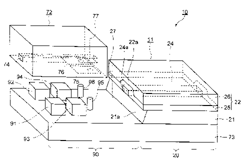
A light waveguide device 10 according to this exemplary
embodiment includes a PLC 11 of the exemplary embodiment and
an LD 72 as an optical element mounted to the PLC 11. The PLC
11 includes a light waveguide part 20 and an optical element
mount part 90. The light waveguide part 20 has a lower clad
layer 21, a core layer 24, and an upper clad layer 22 formed
on a part of a silicon substrate 73 as a substrate. The optical
element mount part 90 has the LD 72, which is to be optically
coupled at a light waveguide end face 27 as an end face of the
light waveguide 20, loaded on the silicon substrate 73. At the
light waveguide end face 27, an end face 21a of the lower clad
layer 21 is recessed with respect to an end face 24a of the core
layer 24 and an end face 22a of the upper clad layer 22 towards
a direction away from the LD 72. The upper clad layer 22 is
configured with an embedding layer 25 for covering the core
layer 24 and a clad layer 26 that is superimposed on the embedding
layer 25.
Next, functions and effects of the PLC 11 and the light
waveguide device 10 according to the exemplary embodiment will
CA 02639638 2008-09-17
be described. At the light waveguide end face 27, the end face
21a of the lower clad layer 21 is recessed with respect to the
end face 24a of the core layer 24 and the end face 22a of the
upper clad layer 22 towards a direction away from the LD 72.
5 Thus, when mounting the LD 72 by bringing it close to the light
waveguide end face 27, the LD 72 does not come in contact first
with the end face 21a of the lower clad layer 21. Therefore,
as shown in FIG. 2, the LD 72 can be coupled to the light waveguide
part 20 without having a gap, so that the optical coupling
10 efficiency can be improved.
FIG. 3 and FIG. 4 are sectional view showing a first
exemplary embodimentof a methodfor manufacturing the PLC shown
in FIG. 1. This exemplary embodiment is a method for
manufacturing the PLC shown in FIG. 1. Thus, explanations will
be provided hereinafter by referring to FIG. 1- FIG. 4.
This exemplary embodiment is a method for manufacturing
the PLC 11 shown in FIG. 1. The PLC 11 includes the light
waveguide part 20 and the optical element mount part 90. The
light waveguide part 20 has the lower clad layer 21, the core
layer 24, and the upper clad layer 22 formed on a part of the
si.licon substrate 73. The optical element mount part 90 has
the LD 72, which is to be optically coupled at the light waveguide
end face 27, loaded on the silicon substrate 73. At the light
waveguide end face 27, the end face 21a of the lower clad layer
21 is recessed with respect to the end face 24a of the core layer
24 and the end face 22a of the upper clad layer 22 towards a
CA 02639638 2008-09-17
11
direction away from the LD 72.
The manufacturing method according to this exemplary
embodiment is characterized to include a fi rst step, a second
step, and a third step described in the followings. In the first
step, the lower clad layer 21, the core layer 24, and the upper
clad layer 22 are laminated on the silicon substrate 73 (steps
A, B, and C in FIG. 3) . In the second step, a part of the lower
clad layer 21, the core layer 24, and the upper clad layer 22
on the silicon substrate 73 is eliminated by using anisotropic
dry etching to form the light waveguide part 20 and the optical
element mount part 90 (step D in FIG. 3 and step E in FIG. 4) .
In the third step, wet etching is applied to the light waveguide
end face 27 by using etchant that exhibits a greater etching
rate for the lower clad layer 21 than for the core layer 24 and
the upper clad layer 22 so as to have the end face 21a of the
lower clad layer 21 recessed with respect to the end face 24a
of the core layer 24 and the end face 22a of the upper clad layer
22 towards the direction away from the LD 72 (step F in FIG.
4).
When eliminating the lower clad layer 21, the core layer
24, and the upper clad layer 22 by using anisotropic dry etching
in the second step, an area in the vicinity of intersecting point
between the face that is etched in parallel to the silicon
substrate 73 and the li.ght waveguide end face 27 that gradually
appears by the etching tends to have a lower pressure. Thus,
an etching gas does not volatilize and tends to stay there. As
CA 02639638 2008-09-17
12
a result, a reaction product film is easily formed on the end
face 21a of the lower clad layer that appears at last by etching,
so that the end face 21a formed into a slope. Normally, a minute
film is used for the lower clad layer 21 so that the core layer
24 does not sink in. Therefore, the dry etching rate thereof
is slow. This helps forming the slop shape of the end face 21a
of the lower clad layer 21. That is, the end face 21a of the
lower clad layer 21 becomes proj ected with respect to the end
faces of the upper clad layer 22 and the core layer 24 towards
a direction approaching to the LD 72.
Thus, in the third step, wet etching is applied to the
light waveguide end face 27 by using etchant that exhibits a
greater etching rate for the lower clad layer 21 than for the
core layer 24 and the upper clad layer 22. With this, the end
face 21a of the lower clad layer 21 becomes more recessed towards
the direction away from the LD 72 than the end face 24a of the
core layer 24 and the end face 22a of the upper clad layer 22.
Thus, when mounting the LD 72 by bringing it close to the light
waveguide end face 27, the LD 72 does not come in contact first
with the end face 21a of the lower clad layer 21 (step G in FIG.
4) . Therefore, it is possible to couple the LD 72 to the light
waveguide part 20 without having a gap, so that the optical
coupling efficiency can be improved.
Next, functions of the exemplary embodiment will be
described in detail. Hereinafter, hydrofluoric acid based
aqueous solutions are generally referred to as "hydrofluoric
CA 02639638 2008-09-17
13
acid".
The silica film that configures the light waveguide part
20 can be etched by hydrofluoric acid. The silica film to which
boronis doped exhibits high etching resistance to hydrofluoric
acid, i. e., it is hard to be etched. When BPSG is compared to
NSG, NSG is etched faster than BPSG. This etching rate ratio
(etching selection ratio) varies depending on the content of
boron and heat treatment temperature of the film. However,
normally, BPSG is not etched faster than NSG.
This is also observed when the light waveguide end face
27 is dipped in a hydrofluoric acid based etchant. That is,
before being dipped in the etchant, the lower clad layer 21 is
projected with respect to the upper clad layer 22. However,
after being dipped in the etchant for a given time or longer,
the upper clad layer 22 becomes projected with respect to the
lower clad layer 21. With this, the lower clad layer 21 does
not become an obstacle when fitting the light emission end face
77 of the LD 72 to the light waveguide end face 27, so that th.e
both can be coupled to each other without having a gap.
FIG. 1 and FIG. 2 are schematic illustrations of the light
waveguide device 10 that is fabricated by passive alignment
packaging. The core layer 24 in the drawings is drawn as a
simple straigh.t waveguide for conveniences' sake. However, in
practice, it is designed diversely for enabling various
functions. FIG. 1 is a schemati.c illustration before the LD
72 is mounted to th.e PLC 11, and FIG. 2 is a sectional view taken
CA 02639638 2008-09-17
14
through the core layer 24 after packaging. As shown in the step
E of FIG. 4, the light waveguide end face 27 is not perfectly
vertical to the silicon substrate 73 as described above, and
it is in a slope shape with the lower clad layer 21 side being
more projected than the upper clad layer 22 side. Therefore,
it is not possible in such a state to completely couple the light
emission end face 77 of the LD 72 to the light waveguide end
face 27 without having a gap.
Thus, a film whose etching rate by hydrofluoric acid is
slower than the lower clad layer 21 is used for the upper clad
layer 22, and it is then dipped in hydrofluoric aci d after the
light waveguide end face 27 is exposed. With this, the lower
clad layer 21 side can be selectively etched as shown in step
F of FIG. 4. As a result, the light emission end face 77 of
the LD 72 and the light waveguide end face 27 can be coupled
without having a gap, at least at the exposed end face of the
active layer 74 and the exposed end face of the core layer 24.
First, each of the steps A- F will be described in more
details. Hereinafter, explanations will be provided by having
buffered hydrofluoric acid (BHF) as preferable etchant for
performing wet etching and having reactive ion etching as
preferable anisotropic dry etching. However, the etchant and
the etching type are not limited to those, as long as it is
possible to achieve the same effects.
(Step A)
First, through the same procedures as those of a typical
CA 02639638 2008-09-17
light waveguide manufacturing method, the lower clad layer 21
is formed on the silicon substrate 73, the core layer 24 is then
formed thereover, and the core layer 24 is processed to a
prescribed shape by photolithography and RIE. Thereafter, the
5 embedding layer 25 for embedding the processed core layer 24
is deposited, and the core layer 24 is embedded by annealing.
Note here that an NSG film having a relatively high softening
point is used for the lower clad layer 21, so that the core layer
24 does not sink in at the time of annealing. Also, an SiON
10 film having a relatively high softening point is used for the
core layer 24, so that it is not deformed by the annealing. In
the meantime, a reflow characteristic is required for the
embedding layer 25, so that a BPSG film having a low softening
point is used for the embedding layer 25.
15 (Step B)
Subsequently, a photoresist film 28 is formed by
photolithography, andthe lower cladlayer 21 and the embedding
layer 25 at a part where the LD 72 is to be loaded are eliminated
by RIE. Here, the core layer 24 is designed in advance so as
not to reach the end face that is exposed by the elimination.
(Step C)
Then, a clad layer 26 of the upper cad layer 22 is formed.
The same BPSG film as that of the embedding layer 25 is also
used for the clad layer 26. This clad layer 26 also functions
as pedestals 91 - 94 at last, so that the film thickness is
determined uniquely. That is, the f ilm thickness is determined
CA 02639638 2008-09-17
16
so that the center axis of the active layer 74 of the LD 72 matches
with the center axis of the core layer 24 of the light waveguide
part 20, when the LD 72 is loaded on the pedestals 91 - 94. If
it is desired to set the sum of the film thickness of the
embedding layer 25 and the film thickness of th.e clad layer 26
to be a prescribed value or more for the characteristic of the
light waveguide, the film thickness of the embedding layer 25
may be adjusted. That is, for thinning the clad layer 26 in
order to lower the pedestals 91 - 94, the embedding layer 25
may be thickened. After forming the clad layer 26, annealing
is applied as necessary.
(Step D)
Subsequently, a photoresist film 29 is formed by
photolithography, and the pedestals 91 - 94, alignment markers
95, 96, and the light waveguide end face 27 are formed by RIE
(Step E) . Here, the core layer 24 is also designed in advance
so as not to reach the light waveguide end face 27 that is exposed
by etching.
(Step F)
Then, those are dipped in an etchant such as BHF, while
keeping the photoresist film 29. At this time, etching of the
NSG film having faster etching rate for the BHF than that of
the BPSG film and the SiON film advances faster. As a result,
only the lower clad layer 21 part of tl-he light waveguide end
face 27 is recessed further.
The dipping time performed at this point is determined
CA 02639638 2008-09-17
17
as follows. First, the etch.ing rates of the etchant for the
lower clad layer 21, the core layer 24, the embedding layer 25,
and the clad layer 26 are obtained experimentally or logically.
Then, based on those etching rates, the time required for the
core layer 24 to be exposed on the surface of the light waveguide
end face 27, and for the lower clad layer 21 part in the light
waveguide end face 27 to be recessed with respect to the upper
clad layer 22 by a prescribed amount is calculated. This
calculated time is the dipping time. The amount of recess from
the exposed light waveguide end face 27 to the end face 24a of
the core layer 24 in the step E is designed by considering the
dipping time. Further, the sizes of the pedestals 91 - 94 and
the alignment markers 95, 96 become smaller because the outer
peripheral parts thereof are etched. Thus, the sizes of those
are also designed by considering it.
(Step G)
Subsequently, necessary steps such as patterning of
metals such as electrodes and passivation of an oxide film for
insulating between the electrodes and the silicon substrate,
although not shown. Thereby, a platform of the PLC 11 is
completed. At last, the LD 72 is mounted to the PLC 11 bypassive
alignment packaging to complete the light waveguide device 10.
As an exemplary advantage according to the invention, at
the end face of the light waveguide part, the end face of the
lower clad layer is recessed with respect to the end face of
the core layer and the end face of the upper clad layer in a
CA 02639638 2008-09-17
18
direction away from the optical element. Thus, when mounting
the optical element by bringing it close to the end face of the
light waveguide part, the optical element does not come in
contact first with the end face of the lower clad layer.
Th.erefore, it is possible to couple the optical element to the
light waveguide part without having a gap, so that the optical
coupling efficiency can be improved.
FIG. 5 is a detailed perspective view showing a second
embodiment of the light waveguide device according to the
present invention before packaging. Explanations will be
provided hereinafter by referring to this drawing. Same
reference numerals are applied to the same components as those
of FIG. 1, and explanations thereof will be omitted.
A light waveguide device 30 according to this exemplary
embodiment includes a PLC 31 of the exemplary embodiment and
an LD 72 mounted to the PLC 31. The PLC 31 includes a light
waveguide part 40 and an optical element mount part 90. The
light waveguide part 40 has a lower clad layer 41, a core layer
44, and an upper clad layer 42 formed on a part of a silicon
substrate 73. The optical element mount part 90 has the LD 72,
which is to be optically coupled at a light waveguide end face
47, loaded on the silicon substrate 73.
At the light waveguide end face 47, an end face 42a of
the upper clad layer 42 has first end faces 42b, 42c, and a second
end face 42d. The end faces 42b and 42c are on a same plane
or almost on a same plane with an end face 44a of the core layer
CA 02639638 2008-09-17
19
44. The end face 42d is in a periphery of the end face 44a of
the core layer 44, and it is recessed with respect to the end
face 44a of the core layer 44 in a direction away from the LD
72. That is, the end face 42a of the upper clad layer 42 is
in a U-letter shape when viewed from the above. The upper clad
layer 42 is configured with an embedding layer 45 for covering
the core layer 44, and a clad layer 46 that is superimposed on
the embedding layer 45.
In the wet etching step described in the step F of FIG.
4, there are cases where the difference between the etching
rates of the core layer 44 and the upper clad layer 42 cannot
be disregarded. That is, the etching rate of the upper clad
layer 42 becomes so much greater than the etching rate of the
core layer 44 that it cannot be disregarded, depending on
combinations of the materials and manufacturing conditions of
the light waveguide, the type of etchant, etching conditions
(temperature, time, etc) , and the like. In such cases, the core
layer 44 becomes projected wi.th respect to the upper clad layer
42 by the wet etching. Therefore, when mounting the LD 72, the
LD 72 or the proj ected core layer 44 may be damaged because the
acti.ve layer 74 of the LD 72 directly abuts against the end face
44a of the core layer 44.
Thus, the PLC 31 of this exemplary embodiment employs a
following configuration. At the light waveguide end face 47,
there are the end face 44a of the core layer 44 and the end faces
42b, 42c of the upper clad layer 42, the end face 42d of the
CA 02639638 2008-09-17
upper clad layer 42, the end face 41a of the lower clad layer
41, and the end face 41b of the lower clad layer 41 located in
this order from the one closer to the LD 72. Thus, when mounting
the LD 72 by bringing it close to the light waveguide end face
5 47, the LD 72 does not come in contact first with the end face
41a of the lower clad layer 41. Therefore, the LD 72 can be
coupled to the light waveguide part 40 without having a gap,
so that th.e optical coupling efficiency can be improved. Here,
the LD 72 comes in contact first not only with the end face 44a
10 of the core layer 44 but also with the end faces 42b, 42c of
the upper clad layer 42, so that the impact when th.e LD 72 comes
in contact with the light waveguide end face 47 can be dispersed.
Thereby, it is possible to prevent the optical coupling part
of the LD 72 from being damaged by making contact with the end
15 face 44a of the core layer 44. These structures can be designed
broadly depending on the combi.nations of the materials and
manufacturing conditions of the light waveguide, the type of
etchant, etching conditions (temperature, time, etc), and the
like.
20 Further, in this exemplary embodiment, there are two end
faces 42b and 42c of the upper clad layer 42 formed by sandwiching
the end face 44a of the core layer 44, when vi.ewed from the light
waveguide end face 47 side. Thus, even if the light emission
end face 77 as the optical coupling part of the LD 72 has a flat
face, and the LD 72 is brought close to the light waveguide end
face 47 while the flat face is being nonparallel to the light
CA 02639638 2008-09-17
21
waveguide end face 47, the LD 72 comes in contact first not with
the end face 44a of the core layer 44 but with one of the two
end faces 42b and 42c of the upper clad layer 42. Therefore,
damaging of the optical coupling part of the LD 72 by making
contact with the end face 44a of the core layer 44 can be avoided
more securely. Needless to say, the end face 44a of the core
layer 44 may be recessed with respect to the end faces 42b, 42c
of the upper clad layer 42 in a direction away from the light
emission end face 77 of the LD 72 for simply avoiding such
damages.
The shape and the number of the end faces 42b, 42c of the
upper clad layer 42 may be set arbitrarily, as long as their
functions can be achieved. For example, there may be one end
face, or three or more end faces provided by sandwiching the
end face 44a of the core layer 44 when viewed from the light
waveguide end face 47 side.
Next, the manufacturing method of the PLC 31 will be
described byconcentrating onthe pointsthat are differentfrom
the manufacturing method shown in FIG. 3 and FIG. 4. A second
step and a third step in the followings correspond to the second
step and the third step of the manufacturing method shown in
FIG. 3 and FIG. 4.
First, i.n the second step, when eliminating a part of the
lower clad layer 41, the core layer 44, and the upper clad layer
42 on the silicon substrate 73 by using RIE, the center part
of the light waveguide end face 47 including the core layer 44
CA 02639638 2008-09-17
22
is recessed with respect to the peripheral part thereof towards
a direction away from the LD 72. That is, the photoresist film
used in RIE is formed into a U-letter shape when viewed from
the above. The shape (dimension of the recessed part) of the
photoresist film is closely related to the time for dipping into
the etchant in the third step, so that it is designed properly
in advance.
Further, in the third step, etchant exhibiting a greater
etching rate for the upper clad layer 42 than for the core layer
44 is used so as to bring the end faces 42b, 42c of the upper
clad layer 42 in the peripheral part closer to the end face 44a
of the core layer 44, and recess the end face 42d of the upper
clad layer 42 in the center part with respect to the end face
44a of the core layer 44 in the direction away from the LD 72.
The dipping time performed at this point is determined
as follows. First, the etching rates of the etchant of the lower
clad layer 41, the core layer 44, the embedding layer 45, and
the clad layer 46 are obtained experimentally or logically.
Then, based on those etching rates, the time required for the
core layer 44 to be exposed on the surface of the light waveguide
end face 47, for the lower clad layer 41 part in the light
waveguide end face 47 to be recessed with respect to the upper
clad layer 42 by a prescribed amount, and for the end faces 42b
42c of the upper clad layer 42 to be on the same plane or almost
on the same plane with the end face 44a of the core layer 44
is calculated. This calculated time is the dipping time.
CA 02639638 2008-09-17
23
Thereby, at the light waveguide end face 47, there are
the end face 44a of the core layer 44 and the end faces 42b,
42c of the upper clad layer 42, the end face 42d of the upper
clad layer 42, th.e end face 41a of the lower clad layer 41, and
the end face 41b of the lower clad layer 41 located in this order
from the one closer to the LD 72.
FIG. 6 is a detailed perspective view showing a third
embodiment of the light waveguide device according to the
present invention before packaging. Explanations will be
provided hereinafter by referring to this drawing. Same
reference numerals are applied to the same components as those
of FIG. 1, and explanations thereof will be omitted.
A light waveguide device 50 according to this exemplary
embodiment includes a PLC 51 of the exemplary embodiment and
an LD 72 as an optical element mounted to the PLC 51. The PLC
51 includes a light waveguide part 60 and an optical element
mount part 90. The light waveguide part 60 has a lower clad
layer 61, core layer 64, 68, 69, and an upper clad layer 62 formed
on a part of the silicon substrate 73. The optical element mount
part 90 has the LD 72, which is to be optically coupled at a
light waveguide end face 67, loaded on the silicon substrate
73.
The core layer 64 is a first core layer that is optically
coupled to the LD 72. The core layers 68 and 69 are second core
layers that are not optically coupled to the LD 72. At the light
waveguide end face 67, the end faces 64a, 68a, and 69a of the
CA 02639638 2008-09-17
24
core layers 64, 68, and 69 are on a same plane or almost on a
same plane, and each of those end faces is projected towards
a direction approaching to the LD 72 with respect to the end
face 62a of the upper clad layer 62 in the periphery of each
of the end faces 64a, 68a, and 69a. That is, each of the three
end faces 64a, 68a, and 69a of the core layers 64, 68, and 69
is in a form that is proj ected towards the optical element mount
part 90, when viewed from the above. The upper clad layer 62
is configured with an embedding layer 65 for covering the core
layer 64, and a clad layer 66 superimposed on the embedding layer
65.
In the wet etching step described in the step F of FIG.
4, there are cases where the difference between the etching
rates of the core layer 64 and the upper clad layer 62 cannot
be disregarded. That is, the etching rate of the upper clad
layer 62 becomes so much greater than the etching rate of the
core layer 64 that it cannot be disregarded, depending on
combinations of the materials and manufacturing conditions of
the light waveguide, the type of etchant, etching conditions
( temperature , t ime , etc ), and the 1 ike . In such cases, the core
layer 64 becomes proj ected with respect to the upper clad layer
62 by the wet etching. Therefore, when mounting the LD 72, the
LD 72 or the proj ected core layer 64 may be damaged because the
active layer 74 of the LD 72 directly abuts against the end face
64a of the core layer 64.
Thus, the PLC 51 of this exemplary embodiment employs a
CA 02639638 2008-09-17
following configuration. At the light waveguide end face 67,
there are the end faces 64a, 68a, 69a of the core layers 64,
68, 69, the end face 62a of the upper clad layer 62, and the
end face 61a of the lower clad layer 61 in this order from the
5 one closer to the LD 72. Thus, when mounting the LD 72 by
bringing it close to the light waveguide end face 67, the LD
72 does not come in contact first with the end face 61a of the
lower clad layer 61. Therefore, the LD 72 can be coupled to
the light waveguide part 60 without having a gap, so that the
10 optical coupling efficiency can be improved. Here, the LD 72
comes in contact first not only with the end face 64a of the
core layer 64 as the first core layer but also with the end faces
68a, 69a of the core layers 68, 69 as the second core layers,
so that the impact when the LD 72 comes in contact with the light
15 waveguide end face 67 can be dispersed. Thereby, it is possible
to prevent the optical coupling part of the LD 72 from being
damaged by making contact with th.e end face 64a of the core layer
64. These structures can be designed broadly depending on the
combinations of the materials and manufacturing conditions of
20 the light waveguide, the type of etchant, etching conditions
(temperature, time, etc), and the like.
Further, in this exemplary embodiment, there are two end
faces 68a, 69a of the core layers 68, 69 as the second core layer
formed by sandwiching the end face 64a of the core layer 64,
25 when viewed from the light waveguide end face 67. Thus, even
if the light emission end face 77 as the optical coupling part
CA 02639638 2008-09-17
26
of the LD 72 has a flat face, and the LD 72 is brought close
to the light waveguide end face 67 while the flat face is being
nonparallel to the light waveguide end face 67, the LD 72 comes
in contact first not with the end face 64a of the core layer
64 but with one of the two end faces 68a and 69a of the core
layers68,69. Therefore, damaging of the opticalcoupling part
of the LD 72 by maki.ng contact with the end face 64a of the core
layer 64 can be avoided more securely. Needless to say, the
end face 64a of the core layer 64 may be recessed with respect
to the two end faces 68a, 68a of the core layers 68, 69 in a
direction away from the light emission end face 77 of the LD
72 for simply avoiding such damages.
The shape and the number of the end faces 68a, 69a of the
upper clad layers 68, 69 maybe set arbitrarily, as long as their
functions can be achieved. For example, there may be one end
face, or three or more end faces provided by sandwiching the
end face 64a of the core layer 64 when viewed from the light
waveguide end face 67 side.
Next, the manufacturing method of the PLC 51 will be
described by concentrating on the points that are different from
the manufacturing method shown in FIG. 3 and FIG. 4. A first
step and a third step in the followings correspond to the first
step and the third step of the manufacturing method shown in
FIG. 3 and FIG. 4.
First, in the first step, the core layer 64 as the first
core layer 64 and the core layers 68, 69 as the second core layers
CA 02639638 2008-09-17
27
are formed simultaneously with a same material. For this, the
mask for exposing the photoresist film in the first step may
simply be changed. This photoresist film is used when etching
the core layers.
Further, in the third step, etchant exhibiting a greater
etching rate for the upper clad layer 62 than for the core layers
64, 68, 69 are used, so that the end faces 64a, 68a, 69a of the
core layers 64, 68, 69 are on a same plane or almost on a same
plane, and that the end faces 64a, 68a, 69a are projected with
respect to the end face 62a of the upper clad layer 62 towards
a direction approaching to the LD 72. The etching rates in the
third step are in a relation of "core layers 64, 68, 69 < upper
clad layer 62 < lower clad layer 61".
The time for dipping to the etchant is determined as
follows. First, the etching rates of the etchant of the lower
clad layer 61, the core layers 64, 68, 69, the embedding layer
65, and the clad layer 66 are obtained experimentally or
logically. Then, based on those etching rates, the time
required for the core layers 64, 68, 69 to be exposed on the
surface of the light waveguide end face 67, and for the lower
clad layer 61 part in the light waveguide end face 67 to be
recessed with respect to the upper clad layer 62 by a prescribed
amount is calculated. This calculated time i.s the dipping time.
Thereby, at the light waveguide end face 67 after the third
step, there are the end face 64a, 68a, 69a of the core layer
64, 68, 69, the end face 62a of the upper clad layer 62, and
CA 02639638 2008-09-17
28
the end face 61a of the lower clad layer 61 in this order from
the one closer to the LD 72.
While the present invention has been described above by
referring to each of the exemplary embodiments, the present
invention is not limited to those exemplary embodiments.
various changes and modifications that occur to those skilled
in the art may be applied to the structures and details of the
present invention. Further, it is to be understood that the
present invention includes combinations of a part of or the
whole part of the structures described in each of the exemplary
embodiments.