Note: Descriptions are shown in the official language in which they were submitted.
CA 02639978 2013-03-06
METHODS FOR LOW COST MANUFACTURING OF COMPLEX LAYERED
MATERIALS AND DEVICES
FIELD OF THE INVENTION
15 This invention relates generally to the manufacture of complex
layered materials
and devices having one or more layers of suitably modified, altered or applied
material.
More particularly, the present invention relates to methods of manufacturing
these
materials and devices at a low cost, in variable volumes and at the same time
with a
high degree of variability and precision complexity under varying degrees of
manual or
20 automatic control. Moreover, this invention further relates to methods
that allow efficient
manufacture of layered materials and devices of differing functionality and
complexity
using the same manufacturing facility. The field of this invention also
extends to the
efficient manufacture of complex polymeric materials and devices, with
manufactured
features of variable and controlled size from centimeters to nanometers.
BACKGROUND OF THE INVENTION
In the discussion that follows, reference is made to certain structures and/or
methods. However, the references should not be construed as an admission that
these
structures and/or methods constitute prior art. Applicants expressly reserve
the right to
demonstrate that such structures and/or methods do not qualify as prior art.
Many industries have moved to layered materials to take advantage of the
increased material characteristics and functionality provided by such
composite
materials. A simple example is the weather protection that paint provides for
the
strength that steel provides. A complex example is the miniature fluid
channelling and
micro reaction chambers made possible by bonding layers of etched and cut
planar
CA 02639978 2008-07-23
WO 2007/085043 PCT/AU2007/000061
sheets of appropriate materials. Another complex example is the production of
multiple
layer printed circuit boards allowing much more complex circuits than were
ever
possible with single or dual layer materials. Another example is the bonding
of
supporting layers to delicate fabrics thereby increasing their durability
without sacrificing
texture and visual appeal. An example of a layered multi-functional device is
the
"SMART" card wherein many layers incorporating graphics, electronics,
magnetics, and
tactile features are incorporated into the one multi-layered device.
Much effort has been put into developing new processes to facilitate higher
productivity and lower cost manufacturing of such composite layered materials.
Over
time, two streams of basic process engineering have developed. One method has
concentrated on individual devices and streamlined the processes to layer or
laminate
complexity and/or functionality. The other method has concentrated on mass
production
of a long layered sheet from which individual devices are excised after
modification.
Each of these methodologies have their advantages. The first methodology
allows materials and devices of high complexity to be manufactured, but at
high cost.
The other methodology allows materials and devices to be mass produced at a
lower
cost, but with a concomitant reduction in complexity.
Further deficiencies and impediments in these methods create production
compromises which further hinder attainment of the goal of low cost mass
production of
complex layered devices. Attempts have been made to combine these processes to
achieve these aims but with varying and limited success.
Polymers have been used as a cheaper alternative to metals for manufacturing
consumable devices especially since the 1940's and have been used for mass
producing complex materials and devices for instrumentation since the early to
mid
1990's. Since the use of polymers in low cost mass production is predominant,
this
discussion concerns the use of polymers, but applies equally to the use of
other
materials, including metals, metal oxides, metal foils, ceramics, glasses and
thin or thick
film surface coatings of these materials or combinations of them.
As well as the two main general process methodologies discussed above,
surface feature fabrication techniques developed in the latter part of last
century
generally can be classified into two further categories.
The first is using direct machining methods in which the pattern of desired
features is created directly on the surface of a stratum made of a suitable
material.
These methods include micromilling, laser based lithography and beam scanning,
plasma etching, wet chemical UV lithography using photoresists, soft
lithography, x-ray
2
CA 02639978 2008-07-23
WO 2007/085043 PCT/AU2007/000061
lithography and print-head deposition. Of these techniques, laser based
processes have
shown the most development due to the ease of processing and their ability to
generate
spatially confined sub-micron sized anisotropic features in a variety of
materials.
The second methodology involves processes that use a master template to form
the desired pattern. These feature replication processes, including soft
lithography,
embossing, compression molding, thermoforming, injection molding and reaction
injection molding, and are particularly suitable to use with polymers,
although these
techniques are used with other materials including low melting point metals
and frits.
Most of these approaches to materials or device fabrication are limited to
creating
2-dimensional or 21/2-dimensional structures. The most common of these
approaches
use one or more of Computer Numerical Control (CNC) micromilling, injection-
molding
or hot embossing, which can generate only very limited feature complexity. For
the
fabrication of complex 3-dimensional polymeric parts these micro-structuring
methods
typically require the assembly of several separately produced parts. However,
these are
serial fabrication processes that have alignment challenges when assembling
micro-
parts which lead to further labor-intensive processes with relatively low
throughput and
high associated production costs.
Another recent approach to the fabrication of complex polymeric materials and
devices is the stacking, aligning and bonding of several layers of thin,
already fabricated
strata (films). This layered approach allows the use of relatively simple 2-
dimensional
manufacturing techniques (such as embossing, die cutting, and laser
processing) as
well as established bonding technologies to create complex 3-dimensional
materials or
devices. Such a 3-dimensional design approach is especially suited to high-
volume
manufacturing using reel-to-reel processing as described by Mehalso ("The
Microsystems Road in the USA," Mstnews, Volume 4/02, pp. 6-8 (2002)) and
Schuenemann et al. ("Packaging of Disposable Chips for Bioanalytical
Applications,"
IEEE Electronic Components & Technology Conference, Nevada, USA (2004)).
Market pressures have prompted the development of mass manufacturing
strategies away from traditional fixed production line approaches and towards
flexible
and responsive manufacturing systems to provide speed and rapid adaptation to
meet
market demands. This new manufacturing approach has typically been applied
towards
individual machine flexibility, or where discrete parts are produced on an
assembly line,
towards flexibility in redirecting or reordering the various production line
modules.
However, this is a more difficult proposition for reel-to-reel systems where
the
production line is a continuous process. Although U.S. Patent 4,805,111
describes a
3
CA 02639978 2008-07-23
WO 2007/085043 PCT/AU2007/000061
modularized web system that can allow reconfiguration of the line, the
flexibility of the
system and the complexity of the produced devices are limited due to the
continuous
nature of the supply feed of the source materials when the system is in use.
To date, for layered polymeric device production, only batch, serial or
continuous
reel-to-reel processing techniques have been described.
In a typical batch process a large quantity or a number of products are
fabricated
in a single batch by a serial sequence of processes. In micro-technology,
batch
processing is very common in the fabrication of silicon or glass-based
devices. An
example is the fabrication of an integrated circuit, in which a silicon wafer
is used as the
substrate, and is subjected to a number of subsequent subtractive and additive
techniques to form electronic parts such as gates and transistors within or
upon the
surface of the substrate. After these processing steps are completed, the
devices are
separated and packaged. In another batch process example, polymer bank notes
are
printed using a printing principle in which sheets or coupons containing
several tens of
notes are processed simultaneously and then separated in a final process step.
Recent
techniques combine this printing principle with the embossing of anti-
counterfeiting
micro-features into the surface of the polymer notes.
These batch manufacturing technologies, however, are rather expensive,
especially when involving micro-features. The main industrial applications of
devices
made according to such methods are in high-throughput-oriented products in
large
industrial, scientific and governmental laboratories where the component can
be reused,
therefore the cost is amortized over the device's operational lifespan. For
many
potential applications of miniaturized layered bio-analytical devices,
especially in
disposable parts for point-of-care/point-of-use devices, such high production
costs
cannot be justified.
Batch-based fabrication of layered polymer based devices can be, and is, used
to
form multiple miniaturized devices through a sequence of processes, such as
die
cutting, bonding, milling and laser cutting. However due to the technical
challenge of
miniaturization and the need for such devices to reliably interface to real
world samples
and instruments, layered polymeric devices made this way are typically larger
than their
silicon or glass counterparts and provide unique packaging challenges.
Furthermore,
these batch-based processes can be difficult to automate, making the storing,
handling,
aligning and assembling of the produced micro-parts a commercial and technical
challenge in itself. Consequently the number of devices that can be
economically
fabricated in parallel from a polymer batch-based process is restricted,
making this
4
CA 02639978 2008-07-23
WO 2007/085043 PCT/AU2007/000061
method suitable for only low volume production.
Serial manufacturing is a manufacturing strategy in which manufacturing
processes interact with a succession of single work pieces (or a very small
number of
work pieces). Examples are injection molding, hot embossing, or mechanical
milling.
Whereas each of these processes, widely used in industry, are optimized for
high
throughput, and several automation strategies to link serial processes are
well in place
for conventional products, the cycle times, the complexity and the cost of the
necessarily
highly automated process sequences all increase significantly for micro-
structured
devices. Storing, handling, assembling and aligning micro-parts in a
competitive
industrial environment remain the technical and economical challenges. Serial
manufacturing processes are therefore best for small to medium-size production
series.
A promising alternative to batch and serial manufacturing techniques are reel-
to-
reel, or so called web-based, processes. These are high-throughput production
processes for combining composite polymer laminates used commonly in the
packaging
and printing industries, and have recently been described for complex layered
device
fabrication See Mehalso and Scheunaman et al., discussed above. See, also,
U.S.
Patents 6,803,019 and 6,878,345.
The process according to the present invention utilizes flexible strata
(films)
continuously fed from reels containing the individual devices which are
therefore
fabricated on a continuous substrate. The fabricated devices can then be used
either on
a reel in a similar manner as described in U.S. Patents 6,803,019 and
6,878,345, or
divided into their individual parts, as described by Mehalso, discussed above.
Such web-based production lines tend to be highly automated and therefore very
labor-efficient. The main advantage of processing on such a continuous
automated
system is the high throughput that can typically be achieved at a relatively
low cost.
Although initial investment costs for a web-based production line are higher
than for
serial production, manufacturing costs per product can be very low for a
suitable large-
scale production line.
The main disadvantage of such reel-to-reel production lines is that they are
typically very sensitive to process variations. If a single processing
component on the
line goes out of tolerance or fails, then, due to the continuous nature of the
production
line, all parts passing that point are affected and production is effectively
curtailed.
Stopping the line to fix the problematic part causes the entire production run
to come to
a halt.
The lines are typically dedicated to one specific product, and require large
5
CA 02639978 2008-07-23
WO 2007/085043 PCT/AU2007/000061
investments in setup time and optimization of parameters, particularly when
dealing with
the tight tolerance requirements for devices with micro-features. Due to this
setup time,
the lengths of the web systems and the total effect of misalignment due to
wear and tear
or component failure, there is typically a lot of material waste. Commercial
systems
typically allow for this waste as a fixed percentage add-on cost and the end
price of the
product is varied accordingly. Another disadvantage of a reel-to-reel system
is that the
slowest process in the system limits the speed of the whole production system.
Furthermore, the substrates in a reel-to-reel process need to be flexible to
allow
for the reel handling systems. See, for example, U.S. Patent 6,827,906. This
limits the
thickness of the layers used and the number of layers that can be combined and
still be
handled in such a production line. This presents problems for many layered
material
applications that require larger interfaces to the environment, larger fluid
capacities,
large handling structures, or a higher degree of component strength, or large
numbers
of bonded layers all of which characteristics tend to make the resultant
device very rigid
and therefore severely restrict the suitability of a reel-to-reel production
method.
Another disadvantage of reel-to-reel handling systems is that the substrates
need
to remain in a mostly planar form with external surfaces having little or no
protuberances. As the substrate thickness is also limited by this method, this
imposes
further design constraints on the product, which often require larger 3-
dimensionally
shaped objects to provide functionality, such as interfacing to an external
device or the
provision of internal liquid storage compartments.
The reference to any prior art in this specification is not, and should not be
taken
as, an acknowledgement or any form of suggestion that the prior art forms part
of the
common general knowledge.
SUMMARY OF THE INVENTION
The present invention overcomes the limitations discussed above while
retaining
the advantages, and introduces new methods to remove or substantially reduce
the
deficiencies and impediments.
The present invention relates to methods for low cost, high volume
manufacturing
of complex layered materials and devices that are the result of an innovative
combination of the disparate processes described above and new novel
processes,
which when combined substantially overcome the limitations of current
practices while
retaining advantages and introducing new advantages. Although applicable to
the
production of layered materials using any substrate material and any
subsequent
6
CA 02639978 2008-07-23
WO 2007/085043 PCT/AU2007/000061
material, one embodiment of the invention relates to the production of complex
polymeric devices with at least one layer of material and with functional
features from
centimeters to nanometers. The invention further provides for the introduction
of non-
polymeric materials into the process and provides for the precision placement
of these
materials to allow complex integrated functionality at low cost and high
production
volumes.
According to one embodiment of the present invention, there is provided a
process for manufacturing a device comprising performing at least one web-
based
manufacturing stage and at least one sheet-based manufacturing stage. In a
further
embodiment, there is provided a process for manufacturing a device comprising
performing at least at least one of the web-based manufacturing stage and at
least one
sheet-based manufacturing stage, wherein a plurality of non-bonding processes
are
performed: (a) within at least one or across more than one web-based
manufacturing
stage(s); and (b) within at least one or across more than one sheet-based
manufacturing stage(s). In this embodiment, the plurality of non-bonding
processes
may be performed in a single web-based or a single sheet-based stage, or one
non-
bonding process may be performed may be performed in each of a plurality of
web -
based or in each of a plurality of sheet-based stages, provided that the
process overall
comprises a plurality of non-bonding stages in at least one of a single web-
based or a
sheet-based stage or collection of web-based or collection of sheet-based
stages which
make up the overall process.
In some embodiments, the process is modular, the processes may be performed
by a plurality of modules and each module may be controlled independently. By
'non-
bonding stage' is meant a process that does not bond (e.g., join or mate) the
parts from
the continuous line and the parts from the sheet (or discrete) line together.
One example
is lamination.
Some modular embodiments comprise a plurality of modules from which a
particular module may be chosen depending on the production history and nature
of the
product being manufactured. Modules may also be interchangeable as required
and
may be capable of receiving or passing materials to another processing module.
The process according to this embodiment of the invention is capable of
manufacturing a wide variety of devices, which may, for example, comprise one
or more
of: a) a layered device, b) a smart card c) a sensor or actuator, d) an
electronic device,
e) an in vitro diagnostic device, or f) a microfluidic device.
A manufacturing process according to the first embodiment of the invention has
7
CA 02639978 2008-07-23
WO 2007/085043 PCT/AU2007/000061
many advantages. For example, it simplifies changes in production strategies
by
increasing flexibility, improves line handling and reduces waste.
A process according to this embodiment of the invention may further comprise a
control system which may optionally be within a module or between a plurality
of
modules. In some embodiments, each module is controlled independently.
Furthermore, at least part of the process according to the present invention
can be
subjected to at least one of a distributed control system or a distributed
monitoring
system.
Routing, re-routing or directing of components in processes of the invention
may
be done by a suitable technique or device. In an embodiment, at least part of
the device
is assembled and/or stored on the manufacturing line. Furthermore, in some
embodiments, components are directed during manufacture according to their
identity.
Thus, in one embodiment, a code may be added (for example, attached) to
components
and the code provides the identity of the components. In addition, components
may be
added to or removed from other components depending on their identity.
In another embodiment of the invention, there is provided a process in which
there is provided in at least one module, use of a reel-to-reel process and in
at least one
other module, use of a sheet-based process to manufacture one or more aspects
of the
device. Such an embodiment is suitable for manufacture of a wide range of
devices.
For example, it may be suitable for manufacturing at least one of a) layered
devices, b)
smart cards c) sensors/actuators, d) electronic devices, e) IVD devices, and
f)
microfluidics devices.
A process according to the present invention may be used to make any suitable
product. In one embodiment, it is used to make laminar products. Such laminar
products may be of any suitable type. Furthermore, it may be adapted to
manufacture
complex products which optionally comprise: a plurality of materials, such as
polymers,
wood, paper, silicon, ceramics, and/or metals; and/or a plurality of shapes
and/or
thicknesses of material and/or preformed components.
In other embodiments, the process is such that it enables a device or
component
which is the subject of manufacture to pass at least one module or station a
plurality of
times. Furthermore, a device or component which is the subject of manufacture
may
travel in a plurality of directions along the manufacturing line and
optionally either
independently of the remainder of the production process.
Various types of device may be manufactured by a process according to the
present invention, including folded devices.
8
CA 02639978 2008-07-23
WO 2007/085043 PCT/AU2007/000061
The process of the invention may also additionally comprise at least one
buffering
station to handle buffer stock. It may also comprise a plurality of production
arms and at
least one production arm may comprise a plurality of processes.
According to another embodiment a laminar device is manufactured which is a
diagnostic device, and in one embodiment, it is a microfluidic device. Various
types of
devices may be manufactured in this way, including folded devices which may
for
example be folded microfluidic devices.
Machining processes also form part of the present invention and one
embodiment comprises multi-layer processing wherein a machining pattern is
created
on a plurality of layers. A sacrificial layer may also be used for machining,
optionally
when the machining is double sided.
In other embodiments, embossing is combined with at least one other process to
improve structure replication. For example, it may comprise the use of cut-
outs,
undercuts, laser processing or any other suitable process.
Optical-based alignment systems also form part of the invention and may
comprise diffractive optics, or the use of interference patterns such as moire
patterns or
any other suitable optical system.
Conductive elements may be incorporated into the device as part of the process
of the invention. Such conductive elements may conduct heat or electricity. In
one
embodiment in which electrodes are added to the device, they are positioned so
as to at
least partially overlay a smart card carrier module. Conductive elements are
added by
various techniques and device, for example, hot foil stamping, interdiffusion
or a printing
technique.
Other processes may optionally incorporate at least one waveguide into the
device. Any suitable technique may be used, for example: surface coating, by
filling at
least one preformed structure, by inserting at least one preformed component.
Suitable bonding processes for use with the present invention may include: use
of at least one structural layer to minimize or avoid structure deformation, a
mechanical
interlocking technique or a surface modification technique.
According to another embodiment, the web-based (reel-to-reel) and sheet
processes are used at different stages of production depending on the
characteristics of
the required process. This embodiment is particularly useful when production
of certain
types of product may require a step which can only be done by one or the other
of these
processes.
In another embodiment, there are provided a plurality of modules from which a
9
CA 02639978 2008-07-23
WO 2007/085043 PCT/AU2007/000061
particular module may be chosen depending on the production history and nature
of the
product being manufactured. In another embodiment there are a plurality of
modules
which are interchangeable as required. Preferably such interchange is
automated.
The aspects which may be manufactured according to the reel-to-reel and sheet
processes according to the present invention may be of any suitable type. For
example,
they may relate to the size, shape, functionality, added components,
characteristics,
etc., of the product in question.
According to another embodiment of the invention, one or more of the
processing
modules are capable of receiving or passing materials to another processing
module.
Such processing modules may be of any suitable type, for example, they may be
sheet
or reel-to-reel (feed) handlers, capable of receiving new material and able to
operate
with changes in direction of the material. Similarly, processing modules may
be stations
for conducting one or more processes such as structuring, bonding, printing,
depositing,
cleaning, surface treating, drying, inspecting, etc.
Control over modules according to the present invention may be by any suitable
technique or device. For example, they may be independently controlled, or
they may
be under system control, or the control of another module. Such modules may
also
comprise feedback control systems, for example from different locations along
a
production line.
A modular process according to the present invention has many advantages,
including:
= = facilitating removal and insertion of partially completed
components to
increase productivity and better meet markets demands;
= maintenance and troubleshooting may be performed more easily and
quickly;
= modules may be replaced easily with minimal disturbance to production;
= modules may be shut down without harming the ability to at least
partially
manufacture the product;
= the process may be further optimized;
= it is easier to meet specific customer requirements due to module
independence and system design flexibility;
= less waste of materials;
= higher overall production output;
= increased ability to cope with variations in demand by more readily
sharing
load across multiple production lines;
CA 02639978 2008-07-23
WO 2007/085043 PCT/AU2007/000061
= greater quality control through testing both at system and modular level;
and
= replication of modules improves quality, lowers development and
implementation costs and speeds delivery.
Another embodiment of the invention comprises distributed monitoring and
control systems throughout the process. According to this embodiment,
individual
fabrication stages are self controlled and may inspect and label output
material as
having passed or failed so that subsequent or other disassociated controllers
may read
this information and process the material accordingly.
An advantage of certain embodiments of the present invention is that buffer
stock
of partially completed material can be identified (eg. machine identified) and
later
processed correctly according to this identification without the need for
persistent
computing memory of product process level and location. A further advantage is
that
material can be manually handled and processed and returned to a production
line and
recognized and processed accordingly. Such a system therefore obviates
dedicated
storage and dedicated transfer lines as material is recognized and routed
appropriately
wherever it enters the system. An example of this would be a partially
completed web
based reel loaded production returned to the input point after maintenance and
the
already completed processing stages would recognize and then ignore the web
product
until it reached its next stage in the process, thereby also obviating any
unnecessary
changes to the production line to accommodate the partially complete product.
Another
example would be manual repairs of rejected sheet based material and this
material
could be returned to the production line at any stage and recognized and
routed
accordingly to its next processing stage.
According to another embodiment of the present invention, there is provided a
process for manufacturing a microfluidic device comprising performing at least
one non-
bonding and non-final separating process during at least one web-based
manufacturing
stage and during at least one sheet-based manufacturing stage. The
microfluidic device
so manufactured may, for example, comprise a folded microfluidic device. In
some
embodiments, the process is modular. By 'final part separation' is meant the
stage at
which a device or fabricated component has been separated from other
components or
parts at the end of the component or device assembly.
In another embodiment, there is provided a process which further comprises a
multi-layer laminating step and in another, material from the one or more web-
based
processes is joined to the same side of the same part or, component or device.
11
CA 02639978 2008-07-23
WO 2007/085043 PCT/AU2007/000061
In another embodiment, there is provided a process for manufacturing a multi-
layer device comprising at least one web and at least one sheet-based
manufacturing
stage wherein one or more processes are performed on one or more web-based
stages
provided that such processes are not graphical printing nor cutting the device
for final
According to another embodiment of the invention, there is provided an
apparatus for manufacturing devices, comprising at least one web-based
manufacturing
component; and at least one sheet-based manufacturing component, wherein the
at
least one web-based manufacturing component and the at least one sheet-based
In another embodiment, there is provided an apparatus for manufacturing a
microfluidic device, comprising at least one web-based manufacturing
component; and
at least one sheet-based manufacturing component, wherein the at least one web-
In another embodiment, there is provided a web-based manufacturing module for
manufacturing a device, comprising: a reel configured to transfer a web; a
reel-to-reel
operative means for performing a manufacturing process on the web in relation
to an
In a further embodiment, there is provided a sheet processing module for
manufacturing a device, comprising: a sheet operative means for performing a
manufacturing process on a sheet in relation to an aspect of the device; and
an
In another embodiment of the invention, a product is produced according to a
process or with an apparatus according to the present invention.
In another embodiment, there is provided a process for manufacturing a multi-
12
CA 02639978 2008-07-23
WO 2007/085043 PCT/AU2007/000061
replicate structure. The at least one other process may for example comprise
using cut-
outs, undercuts, laser processing or any other suitable process.
The invention also relates to a process for manufacturing a multi-layered
device
comprising optical alignment of components. Optical alignment may for example
be by
comprise using diffractive optics or interference patterns (such as moire
patterns).
In another embodiment of the invention, there is provided a process for
manufacturing a multi-layered device comprising incorporating at least one
conductive
element into the device and wherein the conductive element is incorporated by
stamping. In another embodiment, a process for manufacturing a multi-layered
device
comprising incorporating at least one conductive element into the device and
wherein
multi-layered circuits are formed on multiple layers of non-conductive
material bonded
together. In a still further embodiment, there is provided a process for
forming an
interconnect and/or a via between conductive elements on a device, comprising
stamping a part of a conductive material through a non-conductive layer.
In another embodiment, there is provided a process for forming an interconnect
and/or via between conductive elements on a device comprising forming a first
conductive layer on a substrate, adding one or more non-conductive materials
onto the
first conductive layer, selectively removing the non-conductive material, and
forming a
second conductive layer onto the non-conductive material at least partially
overlapping
the area of selectively removed non-conductive material.
The invention also includes a process for manufacturing a smart card
comprising
positioning electrodes so as to at least partially overlay a smart card
carrier module.
In another embodiment, the invention relates to a process for manufacturing a
microfluidic device, comprising directing components of the device according
to their
identity. This embodiment may further comprise the step of attaching a code to
the
components, wherein the code provides the identity of the components and
directing
components may comprise adding components to other components and/or removing
components from other components depending on their identity.
In another embodiment of the present invention, there is provided a
multilayered
device comprising at least one stress-relieving structure to decrease
substrate stress.
The structure may relieve stress in any suitable way, for example it may
relieve stress in
a plurality of adjacent devices or within the device. In one embodiment, the
device is a
microfluidic device.
Throughout this specification (including any claims which follow), unless the
context requires otherwise, the word 'comprise', and variations such as
'comprises' and
13
CA 02639978 2008-07-23
WO 2007/085043 PCT/AU2007/000061
'comprising', will be understood to imply the inclusion of a stated integer or
step or group
of integers or steps, but not the exclusion of any other integer or step or
group of
integers or steps.
BRIEF DESCRIPTION OF DRAWINGS
Various embodiments of the present invention will be described with reference
to
the accompanying schematic drawings, wherein like reference characters denote
like
features, and wherein:
Figure 1A represents a generic modular production unit;
Figure 1B illustrates 3x3 production units arranged to form a generic
production
cell;
Figure 2 illustrates two generic production cells with 2x3 production units
connected in series;
Figure 3 illustrates an example web production system for blister pack
forming;
Figure 4A illustrates a generic production cell with 11 production units;
Figure 4B illustrates three of these production cells, with different modular
units,
arranged in a single production line for complex multi layered device
manufacturing;
Figure 5 shows a unidirectional card production line;
Figure 6 shows a sheet and reel production line with a multipass module and
multiple production arms;
Figure 7 shows a sheet and reel bi-directional production line;
Figure 8A shows a sheet and reel bi-directional production line with offline
transportation stages and buffer storage;
Figure 8B shows a sheet and reel production line with production modules
interfaced to process independent transportation stages;
Figure 9A depicts the individual layers of a layered microfluidic device;
Figure 9B shows the top and side views of the combined layers of the
microfluidic
device depicted in Figure 9A;
Figures 10A-10C illustrate an example of a folded laminate device, wherein
Figure 10A shows the side view of a laminated device with a folding region,
Figure 10B
illustrates the folding of the device, and Figure 10C shows the side view of
the folded
device;
Figures 11A-11C show batch or serially fabricated parts, individually or tray
mounted;
Figures 12A and 12B illustrate the joining of an injection molded part to a
card
14
CA 02639978 2008-07-23
WO 2007/085043 PCT/AU2007/000061
device;
Figure 13A illustrates a top view of a microfluidic device with waveguide
components;
Figure 13B illustrates the incorporation of separately fabricated waveguide
components into a microfluidic device;
Figure 14 illustrates embossing of square edges structures;
Figure 15 illustrates embossing large structures with the bulk of the material
removed prior to embossing;
Figure 16A represents a structuring process where the structure is smaller
than
the thickness of the embossed layer;
Figure 16B shows an example where the embossed structure pushes into the
void below the embossed layer;
Figure 17 illustrates combined laser and embossing processes;
Figures 18A-180 show the assembly of a microfluidic structure split over two
layers;
Figure 19 illustrates the lift-off technique applied to a single layer with
two
sacrificial liner layers;
Figures 20A-20D illustrate the use of double sided machining with partial
patterns;
Figure 21 illustrates via formation in a multilayer structure;
Figure 22 illustrates interconnect formation due to diffusion between
laminated
layers;
Figure 23 illustrates a hot foil stamping configuration;
Figures 24A and 24B illustrate the layering of an electrically conductive
tracks
over a device with smart card electrodes, wherein the cross section views show
the
electrical layer and the card component before and after bonding;
Figures 25A and 25B illustrate the top view of a diffraction forming structure
used
for alignment and a side view on diffraction forming structure, respectively;
Figure 26 illustrates the resultant diffraction pattern used for alignment
over
several layers;
Figure 27 shows a moire pattern formed from parallel lines;
Figure 28 shows a moire pattern formed from circular patterns;
Figure 29 illustrates a poorly formed bond from a single step bonding
procedure;
Figure 30 illustrates the same structure of Figure 29 formed in a multi-step
bonding procedure;
CA 02639978 2008-07-23
WO 2007/085043 PCT/AU2007/000061
Figure 31 illustrates the loss of unsupported cut-outs in a machined layer;
Figures 32A and 32B illustrate the use of support materials during the
machining
processes;
Figure 33 illustrates in-plane relief structures between layered devices on
the
same substrate;
Figure 34 illustrates out-of-plane relief structures between layered devices
on the
same substrate;
Figure 35 illustrates a method of mechanical interlocking for bonding
multilayered
materials;
Figure 36 illustrates the filling of channels for waveguide formation;
Figure 37 shows a simple control loop configuration around a process module;
Figure 38 shows a control loop configuration with feedback inside and external
to
the process module;
Figure 39 shows a control loop configuration with feedback around individual
and
multiple processing modules;
Figures 40A-40D show cross sections of a multilayer circuit fabricated by
stamping methods; and
Figures 41A-41C illustrate examples of production lines for the manufacture of
circuits by stamping methods.
DETAILED DESCRIPTION
It is convenient to describe the invention herein in relation to the disclosed
embodiments relating to microfluidic devices. However, the invention is
applicable to a
wide range of situations and products and it is to be appreciated that other
constructions
and arrangements are also considered as falling within the scope of the
invention.
Various modifications, alterations, variations and or additions to the
construction and
arrangements described herein are also considered as falling within the ambit
and
scope of the present invention.
The manufacturing process of the invention overcomes the limitations described
above for batch, serial, and reel-to-reel manufacturing of layered materials
and devices,
by combining reel-to-reel processing technology and sheet handling systems
into a
flexible production strategy that allows the fabrication of planar and non-
planar devices
of arbitrary thickness with precision 3-dimensional surface and internal
features.
Additional novel methods of manufacture are combined to further enhance the
utility of
the invention.
=
16
CA 02639978 2008-07-23
WO 2007/085043 PCT/AU2007/000061
The advantages of such a combined manufacturing process include the ability to
produce a much wider range of thickness in a multilayer device (from thin to
very thick)
and a much wider range of flexibility in a multilayer device (from very
flexible to rigid), all
processed on the one production line using both reel-to-reel based components
and
components from other sources, thereby enabling low cost, mass production of
components and devices that are stronger, can store larger volumes, provide
more
adequate and more configurable interface to external devices and environments
and
contain increased functionality than would otherwise be the case using
existing
technology.
According to one embodiment of the invention, intermediate processes are
performed as separate processes and the outputs stored for later input to
other
processes which can likewise be performed at one speed, which is a different
speed
than the intermediate processes. The various intermediate processes can be
performed
in one continuous high speed reel-to-reel system, and all manufacturing
operations can
be performed on one or more webs at the one speed. Such an embodiment avoids
the
situation in which the entire process must run at the speed of the slowest
operation. This
embodiment of the invention therefore allows the faster component operations
to be
performed at their optimal speed, thus freeing up equipment to be reconfigured
to
perform other operations, while at the same time the remainder of the process
(or at
least the slowest component operations) may run at the speed of its slowest
operation.
Thus, an overall increase in throughput with lower manufacturing cost is
achieved.
In another embodiment of the invention, the produced layered web structures
may be cut, rendered or divided into sheets to accommodate processes which by
their
very nature require batch processing or produce product which is too rigid for
a web
based process. This embodiment enables increased product complexity without
sacrificing the ability to maximize the use of high speed web reel-to-reel
processes. This
"swap" between reel-to-reel and batch processing can be performed at any stage
during
the production process depending on the line configuration and production run
size.
Such a production strategy further reduces costs of small production runs by
allowing
the fabrication of partly completed components that can be finished at a later
stage,
enabling larger efficient production runs of generic base components using
reel-to-reel,
which are then completed with application-specific batch processes. Certain
application-specific processes may complete the generic components separately
due to
various requirements, such as the need for batch based processing (as above)
or
smaller production runs. According to one embodiment, deposition of volatile
reagents
17
CA 02639978 2008-07-23
WO 2007/085043 PCT/AU2007/000061
is delayed to extend the product's shelf life as well as the need for rigid
product.
Similarly, in a further embodiment of the invention, sheet product may be
introduced into a reel-to-reel process to maximize the use of complexities
possible in
some batch based processes while maintaining the overall efficiencies of a web
based
reel-to-reel process.
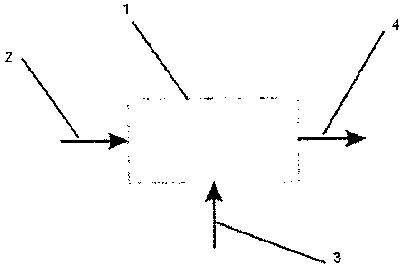
Referring to Figure 1A, a modular production unit (1) performs one or more
production processes having a material input (2), control inputs (3), and an
output (4).
Examples of processing modules include sheet or reel feed handlers, capable of
inserting new material or changing material direction, or stations for
material inversion,
structuring, bonding, printing, deposition, cleaning, surface treatment,
drying, inspection
or other manufacturing processes. A reconfigurable production cell containing
3x3
modular production units is depicted in Figure 1B. In this example, rollers
with optional
unwind units (5) are provided between each production unit (6). The cell shows
three
separate transport lines (7) that may be output to other production units or
cells.
Alternatively, these lines may be combined or split prior to the cell output.
Optional
areas (8) for laminar flow hoods, debris shields, and sheet or reel level
changing are
provided.
An example of a possible configuration for two production cells containing 3x2
production units is depicted in Figure 2. In this example, sheet or reel feed
units (9)
are passed through rotary cutters (10) to the modular unit for structuring,
Printing, or
deposition (11), and then past to a unit for cleaning, surface treating,
drying and/or
inspection (12) before bonding to another layer (13) that has been processed
on a
similar modular line at the bonding station (14). The output from the bonding
station (14)
can be fed into the input of another processing module for further processing.
Alternatively, the outputs (17) of the first 2x3 production cell (15) can be
passed
separately onto the next production cell (16) without prior bonding. Debris
shields or
laminar flow hoods (18) can be provided between each processing line.
Any of the modules may have their own independent control and drivers as well
as being under the system or another module's control. This includes feedback
control
systems from different points within the production line. To further explain
this, an
embodiment comprising a reel-to-reel web production line for forming filling
and sealing
blister packs is depicted in Figure. 3. In this example, the modular
production units
depicted are interspersed with material feed handlers (29) and include:
forming stock
material inputs (19), blister forming (20), filling (21), bonding (22),
printing (23), curing
(24), tension control (25), material guides and unwinds (26), embossing &
perforating
18
CA 02639978 2008-07-23
WO 2007/085043 PCT/AU2007/000061
(27), die cutting (28), and final part collection (30). Production modules
with internal
control systems such as the printing unit (23) ensure that their internal
processes are
optimized, whereas inter-module feedback systems exist to provide optimum
connectivity of the different modules to meet the production line
requirements. An
example of this is the inter-module feedback and control between the tension
control
(25) and its input from the curing unit (24) and the demands from the bonding
module
(22).
The modular, mix and match approach of the invention is further explained with
reference to Figures 4A and 4B. The operations are divided into separated
production
cells, or modules, allowing a reconfigurable production line. The system can
be
configured by altering the interconnectivity between the production cells, or
by altering
production units within each production cell. In this example, the single
common
production cell (31) depicted in Figure 4A contains eleven production units
(32) each of
which can be configured for one or more production processes. Such flexible
processing
stations enable multi-product capabilities within the one production line.
Although the
invention is not limited to production cells of any particular size and/or
number, or to
using production cells or units of the same type, the implementation
illustrated in Figure
4B shows a production line utilizing three production cells (33,34,35) of the
same type,
but with different production units. These modular production units might
represent one
or more production processes such as, but not limited to: sheet or reel
loading (36), reel
loading and course structuring (37), material handling (38), lamination (39),
fine
structuring (40), component and adhesive deposition and curing (42), die
cutting (41),
inversion (43), filling (44), printing (45), and inspection and part
collection (46) stations.
The modular production units can be interchanged as required depending on the
products overall fabrication requirements.
The invention also enables thicker and more complex devices to be fabricated
than with standard web-based systems by allowing both sheet and reel stock to
be
handled on the same line. In Figure 4B, the input (36) can accept both sheet
or reel
stock and the main web-line (47) can operate using both continuous and
discontinuous
production materials. Continuous web-based production of multilayer laminates
has
traditionally required continuous flexible materials to pass through nips and
around roller
guides. The invention overcomes this limitation by allowing rigid, thicker,
and more
complex devices to be fabricated by combining web based and discrete component
handling techniques in the same production line.
Referring to Figures 5, 6, and 7, sheet and reel components are used for the
19
CA 02639978 2008-07-23
WO 2007/085043
PCT/AU2007/000061
production of multi-layered card-based devices on continuous production lines.
Typical
automated card manufacturing and personalisation systems operate either a
batch or
serial production strategy and have been limited to standardized format card
handling
systems. Figure 5 depicts a typical card personalisation process with
input/output
hoppers (48,49) and a card handling systems that accept only ID-1 (ISO 7816)
format
material (50). The processes sequentially operating on the cards include:
printing or
laser engraving (51), overlay laminating (52) of preformed laminates (56),
embossing
(53), topping (54), and finally programming or encoding (55). These systems
typically
use preformed laminates as the cards are of a standard size and customization
is not
required. The invention allows the use of processing stations (other than just
printing) to
produce custom laminates, or other components, that come together from
different arms
of the processing line.
For example, Figure 6 illustrates a card production process with multiple
production arms, and has more than one input feed, of either reels (57,58) or
sheets
(59), which input undergoes processing at various production modules (60) and
are
brought together for further processing. In this embodiment, discontinuous
card
components are laminated with input stock (57,58) that have undergone
processing
prior to lamination. Furthermore, more complex multilayered devices can be
fabricated
by this example, where multiple layers may be added to one part by performing
multiple
laminations at the multipass station (61). Although a degree of flexibility is
provided from
this multiple-pass lamination unit, each layer is limited in its form by the
order of the
processing stations at each line. This limitation can be overcome by providing
a line
design with buffering, or insertion and removal of components between
processing
stations.
Figure 7 provides a bi-directional production line (62) allowing a work-piece
to
travel back and forth to any processing station (63). In this example, the bi-
directional
line (62) has input/output hoppers (64) at either end with two production arms
joining the
bi-directional line from reel stock (65,66). This bi-directional processing
line approach
provides full flexibility but limits the throughput since each processing
station may only
process or pass one part at a time. Thus, a station in use prevents another
part from
passing.
Figure 8A overcomes this limitation by providing one or more fully reversible,
or
bi-directional, lines with one or more transportation stages (68) that are
separate from
the processing line (67) and may move the parts in and out at various stages
along the
line to maximize the line efficiency. The separate bi-directional line (68)
allows parts to
CA 02639978 2008-07-23
WO 2007/085043 PCT/AU2007/000061
pass processing stations that are in use. In the example of Figure 8A, the
production
line is similar to Figure 7 and contains a bi-directional processing line
(67), two
production arms supplied from reel stock (69,70), processing stations (71),
and
input/output hoppers (72,73), with the addition of one or more separate bi-
directional
lines and transportation stages (68) having buffering stations (74).
The example in Figure 8B is similar to Figure 8A but without the bi-
directional
processing line dependent on the processing modules. Instead, the processing
stations
(71) that were along the processing line are only interfaced to one or more
independent
bi-directional transportation stages (68), and the buffering stations (74)
also act as
input/output hoppers. In all of these configurations the use of buffering
stations can be
used to further improve efficiency between individual processing stations.
However,
offline buffering is particularly effective in increasing the entire
production line efficiency
as shown in Figure 8A and 8B where the removal, insertion, and storage of
partially
completed components may be automatically performed at any of the appropriate
processing stations.
According to further embodiments, the approach of the present invention allows
a
flexible robust production line that provides a more thorough testing process
and
improves quality by facilitating testing at both system and at individual
modular levels.
Intra-process testing regimes are not subject to limitations of dwell time
between stages,
as this is no longer a factor in process according to the present invention.
Furthermore,
manual inspection becomes possible for critical components. The detection and
correction of process problems therefore occurs at a stage where, for the most
part, raw
material losses are minimized.
Another advantage of the present invention over conventional systems is that
the
separation and independence of the various modules improves design quality by
allowing the design process to concentrate on functionality and efficiency for
individual
modules, and not compromise these attributes for the sake of connectivity. For
these
same reasons, development and implementation costs are lower and the delivery
of
new modules and therefore the delivery and implementation of new production
lines are
both expedited.
Yet another advantage of the present invention is that failure of a single
part of
the process has a smaller impact on the overall production. If a section or
part of the
process fails in a traditional web based process then the whole process stops,
ie. the
entire production ceases. In the process according to the present invention,
all stages
unaffected by the failure would continue to produce product which would be
temporarily
21
CA 02639978 2008-07-23
WO 2007/085043 PCT/AU2007/000061
stored waiting to be reinserted into the process at the appropriate place. An
additional
benefit of this feature of the invention is a reduction in wasted material. In
current reel to
reel or continuous production systems, ceased production because of failure
causes
most, if not all, material in the entire production line at the time of the
failure to be
compromised and wasted. This is clearly not the case in the present invention.
Another advantage of the present invention is the ability to arbitrarily and
deliberately freeze and store production at a certain penultimate finishing
stage in which
partially completed product may wait until finished product is required (for
example to fill
inventory) and the partially completed sub-components may be reinserted into
the
production process and perishable or sales specific reagents or components,
for
instance, could be added before final finishing and packaging. This feature
would allow
just-in-time production of customer or application specific layered devices
with the
minimal amount of time, lowest cost and the least amount of additional quality
assurance and quality control process.
A further benefit of the present invention is that stages that are not
required for
final finishing may be reconfigured to produce penultinnately finished product
for another
design of layered device, or may be configured to duplicate slower processes
in other
production lines in the same facility thereby maximizing the use of capital
equipment
and improving production efficiency.
Higher overall product throughput is therefore achievable using such a modular
approach for facilities which manufacture small runs of multiple products than
can be
achieved with conventional systems.
Layered device designers may now take advantage of these flexible production
features to further improve design and production flexibility, with
concomitant cost and
marketing advantages, to a stage not previously possible.
A further advantage of the invention is that maintenance and troubleshooting
may
be performed more easily and quickly, as modules can be replaced easily with
minimal
disturbance to production, and certain stages may be shut down for maintenance
allowing partial device fabrication and storage.
Figures 9A and 9B show one embodiment of a layered microfluidic device. The
individual layers of the device (75,76,77,78,79,80,81,82) are illustrated in
Figure 9A,
with the composite top (83) and side (84) views shown in Figure 9B. The layers
may be
fabricated from sheets or reels of continuous material and converted into
either sheets
by machining or into continuous material by bonding to other layers.
Figure 10 illustrates a multilayer device that has two multilayer components
22
CA 02639978 2008-07-23
WO 2007/085043 PCT/AU2007/000061
(85,86) joined by a thin flexible substrate that may be folded along the
flexible region
(87) to bond the two multilayer components together. Alternatively the device
may be a
multi-layer, or multi-component device, with at least one flexible folding
region. The
advantages of fabricating a device or component with a flexible region
include:
- Improved connectivity for electrical, optical and similar components as
there is less need for lossy and failure prone interconnects or vias.
- Improved alignment between components or production processes where
those processes would normally be split over more than one layer. For
example, components can be deposited by one process onto the one layer
using a single reference point and/or tool, and then the layer is folded to
reposition the components on the device.
- Matching processing on layers using the same production process. A
simple example is the fabrication of holes between layers. If split over
several individual layers each process needs to be aligned for each layer.
If using a folded approach then a single tool can be used, referencing the
holes to one another and providing identical processing parameters.
- Reduced production processing by enabling processing on a
single layer
then folding rather than processing on two or more separate layers.
- Simplified handling due to a reduction in the layer count.
In another embodiment of the invention, the structured films are laminated to
other components, which may or may not be a continuous substrate, and may or
may
not be planar, and may be made of single or multiple components. Such
components
could include batch or serially fabricated parts, single or multi layer parts,
individually or
tray mounted, as shown in Figures 11A-C.
The microfluidic part (88) of Figure 11A contains an electrode (89) and
microfluidic (90) components and is shown in Figure 11B as part of a larger
sheet or
web (91) containing multiple parts with alignment holes (92) and sacrificial
joining tabs
(93). Figure 11C shows four microfluidic parts (88) mounted in a carrier tray
(93A) for
passing between processing stations.
According to the present invention layers of material may be attached to other
components by various methods. Preformed layers cut to size may be
individually
bonded to other discrete components (the bonding of individual laminates to
discrete
components). Preformed layers may be delivered to the discrete components on a
carrier layer that has more than one preformed layer, and may be continuous
(the
bonding of individual laminates on a carrier to discrete components). The
layers may be
23
CA 02639978 2008-07-23
WO 2007/085043 PCT/AU2007/000061
delivered to the discrete parts as a continuous layer with preformed tension
points, such
as perforations or partially cut material, that separate by an applied force
just prior to or
at some point after bonding to the discrete part (the bonding of preformed
self
separating laminates to discrete components). The layers may be delivered to
the
discrete parts as a continuous layer and cut entirely, or partially through
and separated
by an applied force, just prior to or during the bonding stage (forming then
bonding self
separating laminates to discrete components). The layers may be delivered to
the
discrete parts as a continuous layer and separated from the continuous layer
just prior
to or during the bonding stage (forming then bonding laminates to discrete
components).
The layers may be delivered to the discrete parts as a continuous layer that
is cut just at
some point after bonding to the discrete part (trimming of the continuous
layer after
bonding to discrete components).
Figures 12A and 12B show one embodiment in which the sheets may be
individual batch or serially fabricated components bonded to the films or
other sheets. In
this embodiment, a relatively thick injection molded part (94) is bonded to a
microfluidic
card (95), providing interface and reagent storage. Figures 12A and 12B show
the two
parts before and after assembly, respectively. The addition of serially or
batch fabricated
parts includes bonding of parts between the layered films as described in the
waveguide
section for optical component integration. An example of this is illustrated
in Figures 13A
and 13B, where the assembly for the microfluidic device of Figure 13A,
containing
preformed waveguides (96) inserted into a substrate (97) containing
microfluidic
structures (98), is shown in Figure 13B. The preformed waveguides (96) are
placed into
locating structures (99) in the substrate (97) adjacent to the microfluidic
structures (98).
A sealing layer (100) is then used to seal the device providing only inlet
ports (101) to
the microfluidic structures on the top surface (102) and waveguide input and
output
through the side ports (103).
Materials used according to the present invention may include non-metallic or
metallic films or sheets as structural or heat conductive layers,
electromagnetic
shielding, or as a part of an integrated component. Structural layers are
important to
avoid channel sag from a bonding process, which is a major problem in larger
microfluidic structures sealed with films, thereby allowing wider channels to
be
fabricated by this 3-dimensional layering strategy.
Heat conductive layers may provide improved thermal control within the device,
which is important for optimising reaction conditions. Electromagnetic (EM)
shielding
protects the sensors and actuators on the disposable device from
Electromagnetic
24
CA 02639978 2008-07-23
WO 2007/085043 PCT/AU2007/000061
Interference (EMI) and in some cases reduces emissions from chip components or
may
be used to strengthen EM fields used for some actuators (as with magnetic and
paramagnetic particle manipulation).
Other materials may also be incorporated into the products including, but not
limited to, paper, nitrocellulose, glass, and fabric based products depending
on the
application requirements.
Of the micro-fabrication techniques mentioned earlier, the methods of die
cutting,
laser processing, embossing, thermoforming, and print-head deposition are all
techniques that may readily be integrated into a reel-to-reel system. With the
process
according to the present invention, other fabrication techniques such as
injection
molding and micromilling may also be incorporated into the manufacturing
process.
The macroscopic injection molding process can be adapted for fabricating micro-
parts by either employing a variotherm process or using a non-thermal
polymerization
method such as with UV reaction molding. The difficulties with micro-injection
molding
are the high pressures and low viscosities required to inject the polymer into
the
microstructures of the mold cavity. With the decreasing size of the
microstructures, the
cycle time and difficulty of manufacture are increased. Due to the
difficulties of ejecting a
component from a mold, fully 3-dimensional microfluidic structures are not
feasible with
this process alone. Instead, typically multiple structures are aligned and
bonded
together to achieve buried channels.
In a similar manner to traditional computer numerically controlled (CNC)
milling,
micro milling employs computer driven milling tools to route a structure.
Micro-mills
operate at higher tolerances and use smaller drill bits than standard CNC
mills (down to
100 m). This is mostly a 2-2.5D technology as buried channels cannot be
fabricated
without bonding other parts over the channels.
Die cutting is a process used to stamp out structures entirely through
substrate
layers. The process involves a tool with defined edges pressing into and
piercing a
substrate against another surface or matching edge. Typically, the structures
achieved
by these methods are large by microfluidic standards, rotary cutters are
usually limited
to structures greater than a millimetre, whereas match platens can achieve
dimensions
down to 100 m.
Most of the work to date on laser micromachining has been performed with
assistance of ultraviolet lasers, mainly with excimer lasers, which can
produce fine
anisotropically etched structures down to one micron. Unfortunately such
systems are
expensive and relatively slow. More recently, focus has been on the use of
shorter
CA 02639978 2008-07-23
WO 2007/085043 PCT/AU2007/000061
wavelength UV lasers that can machine channels down to 10011m, depending on
the
material thickness. Unfortunately these systems provide a large heat-affected
zone that
limits microfluidic geometries. In a similar manner near-IR CO2 lasers have
been
demonstrated for microfluidic channel fabrication for large structures only
(in the order of
hundreds of microns). The challenge in incorporating these technologies into a
web
based system relates to the time required for the laser to complete its
machining
process as well as the morphology of the resulting cut.
Embossing is a technique in which a stamp is pressed into a polymer material
to
form a replicated structure in the polymer. The replicated structure produced
is a
negative image of the stamp. Embossing is capable of replicating structures in
the
submicron domain. However, for larger structures this becomes more difficult
as the
material shifted when embossed is required to flow to other regions within the
bulk
material. Problems of material relaxation and stress after the embossing
process can
cause the replicated structures to deform. This problem is exaggerated for
polymer
films, which are often orientated and are thinner, more rigid substrates.
The hot embossing process is similar to the standard embossing process except
that the temperature of operation is typically close to the material's glass
transition
temperature and the embossing pressures are lower. As with all embossing
techniques
the quality of the replicated structures are dependent on several parameters
including
imprinting pressure, temperature, time and the material properties.
Such embossing techniques typically use flat platens and long residence times
to
achieve high aspect ratio microstructures, and are generally not applicable to
high
throughput reel-to-reel systems for these type of structures. U.S. Patents
6,375,871 and
6,375,776 overcome this limitation by integrating micro-embossing into reel-to-
reel
manufacturing systems by extruding a melted resin onto a film prior to
embossing the
melted material. British Patent GB 9623185.7 discloses a method for using UV-
cured
epoxies extruded and embossed in a similar manner before curing. Problems with
such
systems include the limitation of materials suitable, and therefore available
bulk and
surface properties for the microfluidic device.
Thermoform molding is a method of structuring thermoplastic films by heating
the
film to the softening point of the plastic and then applying force by vacuum
or air
pressure against the film to allow it to form against the mold. This technique
is typically
best suited for structures larger than a couple of hundred micron due to the
difficulty in
achieving sharp corner radii. Very little work has been done in demonstrating
this
technique for microfluidics.
26
CA 02639978 2008-07-23
WO 2007/085043 PCT/AU2007/000061
Print-head deposition is a method for depositing material by a scanning print-
head, such as a syringe, glue gun or inkjet cartridge. These methods include
some of
the rapid prototyping techniques available, such as stereolithography (SLA),
and
selective laser sintering (SLS). These rapid prototyping techniques typically
have
tolerances that are too large for microfluidic applications, however, new
adaptations are
being developed that can form microfluidic structures. Deposition of adhesive
for
channel wall formation is described in U.S. Patents 6,509,085 and 6,074,725.
Lago et
al. produced microfluidic channel walls by laser printing. These systems have
limitations
in terms of the chemical compatibilities of the deposited materials and their
permeabilities.
The process according to the present invention combines reel-to-reel
processing
technology and sheet handling systems in a flexible production strategy to
produce
components incorporating microstructures for fluid, electrical, and optical
control. Such
structured devices may be produced by laminating structured films together,
and/or
laminating films to sheets. The sheets are rigid non-flexible components that
may be
machined by other processes such as hot embossing and injection molding, and
may be
arranged as single components or multiple components forming trays.
The films may be structured by processes including, but not limited to,
embossing, laser processing, die cutting, or thermoforming. Each of these
techniques
have there own associated design rules for optimal structuring. These design
rules
include, but are not limited to, limiting sharp edges, such as sharp corners
in fluidic
channels, order of processing, and numerous other operational parameters such
as
speed, temperature, pressure, tension, etc. None of these processes have yet
been
integrated on a reel-to-reel process for the mass manufacturing of complex
microfluidic
devices.
For low cost, high throughput manufacturing the following considerations can
be
used to demonstrate the structuring technologies applicability depending on
material
type, size, and processing parameters;
= Roller cutting is only suitable for very large structures >1000 m
= Match stamp die cutting may be used with complicated tools for
large structures >>200 m
= Excimer laser processing is relatively slow and is only suitable for
very fine quickly ablated structures >1 m with small total area
coverage.
= Cheaper direct write IR laser technologies are only suitable for
27
CA 02639978 2008-07-23
WO 2007/085043 PCT/AU2007/000061
larger structures and where melt zone can be tolerated >>20012m.
= Film embossing is typically best for fine structure replication <10 m
depending on volumes of material displaced
Of these techniques, embossing represents the cheapest manufacturing
alternative, but is severely limited dimensionally for films, or even bulk
materials at high
speed. According to one embodiment of the invention, the process combines
embossing
with other techniques to improve embossing capabilities and overcome some of
the
limitations of the other structuring methods. This allows embossing of
structures of all
sizes and improved channel geometries over conventional techniques.
The layering technique for forming 3-dimensional microfluidic devices
typically
involves layering of gasket shaped films, and producing channel structures
that have
square or rough edges. Restructuring these edges by embossing allows other
geometries for improved hydrodynamic flow and device functionality.
Figure 14 illustrates the embossing of a square edge channel to produce a
channel geometry with a rounded cross section. In this example the layer with
a square
edge channel (105) is bonded onto another layer (106), that is more rigid at
the
embossing temperature, and an embossing tool (107) with a rounded edge is
brought to
bear on the channel structure. When the tool (109) is mated with the
structured layer
(108), the softer material forms around the tool structure. Upon separation of
the tool
(104) the structured layer (110) shows an embossed structured replicate of the
tool.
In a similar manner, large embossed structures may be formed by removing the
bulk of the material inside the structured area, ensuring less material is
required to be
shifted during the embossing processes. This allows embossing of much larger
structures without long stamp residence times or inducing large material
stresses. The
embodiment of Figure 15 illustrates the embossing of a multilayer structure
(111) where
the bulk of the material in the structured area (112) was removed by processes
prior to
embossing with a tool (113). During embossing, the structured material (114)
forms
around the tool (115), leaving a formed image of the tool (116) in the
structured material
(117).
Another advantage of the invention is that the swarf and rough edges produced
by the cutting processes, such as laser and die cutting, may also be embossed
after
structuring to improve channel performance. In these cases the swarf, debris
and
roughened edges of the machined surfaces can be embossed and reshaped into the
bulk structure to provide cleanly structured surfaces.
Another process according to the present invention for improving the
replication
28
CA 02639978 2008-07-23
WO 2007/085043
PCT/AU2007/000061
of structures in films is the use of undercut layers below the embossed
structure to allow
the displaced material to be shifted out of the way rather than into the
surrounding bulk
material, as illustrated in Figures 16A and 16B. The embossed material may
have a
lower glass transition temperature than the material below with the undercut.
The
layered components shown in both figures have an embossing layer (118), a
layer (119)
containing a relief structure (121), or undercut, and a bottom layer (120)
with an air vent
(122). The volume of undercut (121) may be calculated to match the displaced
material
to ensure good replication against the mold, and either an air vent (122) or
air reservoir
may be used to reduce the backpressure in the undercut from the air
compression.
Figure 16A represents this structuring process where the structure is smaller
than the
thickness of the embossed layer, the tool (123) is pressed onto the embossing
layer
causing the tool structure (124) to embossing part-way through the embossing
layer
displacing some of the material from layer (118) into the pressure relief
structure (121).
A similar example is shown in Figure 16B where the tool structure (124) is
taller than the
depth of the embossing layer (118), and the resulting embossed structure
pushes into
the void below the embossed layer.
These methods allow much larger replication of embossed structures than is
normally achievable in film-based devices, and particularly those materials
that are not
entirely amorphous. The process also provides a method for shorter residence
times in
comparison to normal embossing as only the area in the proximity of the
feature needs
to be heated to allow reflow. In comparison to the hot embossing process where
the
entire bulk of the material is required to be heated to allow material flow,
or in standard
embossing processes where more material is required to be shifted causing
larger
intrinsic stresses in the material.
The laser embossing process according to the present invention enables more
rapid replication of embossed features than by normal and hot embossing. By
pre-
treating the local area to be embossed with lasers the local material is
altered, which
allows (a) a reorganisation of the localised material structure and for some
polymers a
lowering of the softening point (as is especially the case with orientated
films), (b)
preheating of the exposed area, (c) material reflow and (d) in some cases,
ablation or
material removal from the embossed area. Before stamping the area of the film
to be
treated, the local area or the tool may be heated to improve the material flow
around the
tool. The laser beam may expose the entire substrate surface or just the area
to be
embossed. Automated systems may also be used to guide the laser beam in an
appropriate pattern either by computer file direction or from image
recognition off the
29
CA 02639978 2008-07-23
WO 2007/085043 PCT/AU2007/000061
tool or material. Figure 17 illustrates a focused laser beam (125) scanned
over
amaterial (126) prior to embossing with a tool (127) into the exposed area
(128). Upon
contact with the tool the irradiated material (129) forms around the tool,
leaving a
structured surface (130) when separated. In a similar manner other material
treatments,
such as the chemical, corona and UV treatments discussed later, can be used to
modify
the materials properties near the embossing area to enhance the embossing
process.
Such a process allows the use of longer wavelength lasers than the expensive
and slower UV excimer systems for fine structure formation. Unlike their
excimer
counterparts, such longer wavelength systems produce more thermal damage and
typically have larger focus spot sizes, which severely limits their spatial
resolution for
micro-structuring and provides poor cut quality. By combining the laser
processing with
embossing, finer and more accurately formed microstructures may be fabricated
than
with the laser alone, and faster residence times and larger structures may be
formed
than with embossing alone, thereby providing a much faster and cheaper method
than
excimer laser processing. A process according to this feature of the invention
is also
compatible with reel-to-reel systems.
The die stamping approach according to the present invention separates large
fluidic structures over multiple layers. This approach allows the
implementation of a
modular stamping process having a similar form to a "printing press", i.e. a
die with
modular and interchangeable stamping tools. Without a layered process,
discontinuities
between each modular stamping tool might provide blockages in formed channels.
Figure 18A illustrates two layers that have been stamped with parts of a
fluidic structure
(133) over two separate layers (131,132). The first layer shows three
discontinuous
fluidic elements that can be joined by the layering of the second structured
layer.
Figures 18B and 18C illustrate how these two layers (131,132) may be aligned
on top of
one another and bonded together to form a single layer (134) with a continuous
fluidic
structure (135).
Alternatively, a single layer approach may be used if embossed interconnects
are
made between the holes made from the modular stamping tools.
Furthermore, a layered approach may also be used to avoid misalignment within
the structures of a layer due to some geometries providing freedom of
movement, as
covered in U.S. Patent Application Publication 2002/0112961 Al for structure
geometries having angles substantially greater than 90 .
The lift-off technique is a common technique used in film converting to
process
(stamp, roller and laser cutting, etc.) the film with its liner layers
attached, and then just
CA 02639978 2008-07-23
WO 2007/085043 PCT/AU2007/000061
prior to bonding to remove these liner layers. This method ensures the film is
kept clean
prior to bonding and can aid in the removal of swarf and other related debris.
In laser
processing such liner layers may help improve the cut quality by removing any
formed
ridges and removing the first and last surface affected by lasering. It is at
these
boundary layers where the heat conduction is essentially 2-dimensional, as the
cut
deepens and the laser enters the bulk of the substrate, the heat conduction
becomes
essentially 3-dimensional, giving a smaller heat affected zone. Bonding the
substrate, or
substrates, liner layer to a relatively large surface may provide further heat
conduction
and ease of waste removal for improved processing.
Figure 19 illustrates an example of the use of the lift-off technique during a
laser
structuring process. The substrate to be machined (136) is bonded to one or
more
sacrificial layers (137,138), machining is performed, and the sacrificial
layers are
removed leaving the cleanly structured substrate (139). Furthermore, this
technique may
be used to provide contact masking of a substrate to allow the patterned
exposure of the
substrate to other processes as described in this invention.
The automated application and use of protective, carrier, and or masking
layers
to a material can be provided for by the invention. To overcome the
limitations of
material handling for the removal of the aforementioned layers, the invention
employs
double-sided processing using split patterns. Processing a material from more
than one
side using different parts of a single pattern can provide careful control
over material
cut-outs and discontinuities. By controlling the amount of material attached
in each cut
out area on each layer, the material in a cut-out area can be removed with the
removal
of one or more layers. For example, the pattern of Figure 20A provides three
cut-outs
areas (140,141,142). If a material was entirely machined through with this
pattern then
all these cut-outs would be unsupported. Furthermore, the outer layers would
then be
discontinuous, making the removal of sacrificial layers or waste areas
problematic
above the cut-outs or discontinuities. If the entire pattern were machined
through a layer
of the multilayered device, then the subsequent removal of the outer layer
would not
remove the entire patterned area. By providing outer sacrificial layers and
machining
from both sides with a discontinuous pattern then selected layers can be
removed
entirely and still provide a completely machined internal layer (143). As can
be seen with
the cross section shown in Figure 20B, the two outer layers (144,145) are only
partially
machined and the center layer (143) is completely cut through along the
machined
pattern.
Double sided processing can occur at separate processing stations on either
side
31
CA 02639978 2008-07-23
WO 2007/085043
PCT/AU2007/000061
of the material, or the material may be flipped and passed through stations on
the same
side. In one embodiment of the invention, shown in Figure 20C, material
handling rollers
(151) are used to manipulate the sheet and reel materials allowing the
substrate
material (146) to be reversibly bonded to two protective layers (147,148) fed
from reels
(149) onto the substrate's (146) top and bottom surfaces prior to structuring
by the
stations (150). After processing at one or more stations (150,151) the
protective layers
(147,148), with their cut-out zones attached (140,141,142) are then removed by
the
unwind reels (152), leaving the discrete parts (153).
In another embodiment of the invention, a material is processed into smaller
discrete components but handled as a continuous material attached to one or
more
carrier layers or parts. Referring to Figure 20D, only one protective layer
(154) is
removed to allow the continuous handling of the material and bonding onto a
new
component or carrier layer (158), then the second sacrificial layer (155) is
removed.
With the result leaving cleanly processed parts (157) having their cut-outs
removed, and
bonded a new component or carrier layer (158).
Other techniques that may be combined, or used separately, with the
aforementioned methods to improve the cut quality and remove debris include:
O Oven heating
O Flash heating
0 Laser scanning
(lower energy or faster scan rate to clean rather
than etch substrates)
O Air jets
O Chemical baths
O Mechanical knives
Conductive circuits on polymer substrates are usually made via etching, screen
printing, or electroplating processes.
Etching is used in the printed circuit board (PCB) industry for the
manufacture of
flexible electronic circuits. Typically, copper coated polyimide is coated in
photoresist,
which is then patterned and the resulting pattern is then etched away
chemically. The
main disadvantages of this method are the limited material types of the
substrate and
conductor available.
Printing is easily implemented in production, has low tooling costs, and
allows a
reasonably wide range of materials to be used. Printing technologies include
channel
filling, contact mask, screen printing, flexography, gravure and printing.
Issues to be
considered with the process include the limited material thicknesses (<25 m)
and
32
CA 02639978 2008-07-23
WO 2007/085043 PCT/AU2007/000061
inability to solder to the resultant electrodes.
Electroplating or electroless plating is more difficult to implement in
production,
but enables excellent control of spatial resolution (>101.1m) and can be
plated to almost
any thickness depending on the exposure time, and is well established in the
PCB
industry. Methods of forming seed layers include wet chemical priming and
plating, laser
ablation deposition, ebeam evaporators, physical vapor deposition (PVD) and
chemical
vapor deposition (CVD) techniques.
The process according to the present invention uses layers of structured
polymer
films and sheets to form sophisticated fluid handling devices. In those
embodiments
which relate to the use of electrodes within these devices it becomes
necessary to
provide techniques for providing interconnection between the internal and
external
electrodes, which may require vias through various layers and interconnections
between
layers.
Interconnects and vias in polymer films have been extensively developed for
the
flexible PCB industry in which through-hole electroplating and riveting are
used to
provide connection through and between each layer. See, for example, U.S.
Patent
Application Publication 2001/0047880 Al. Through hole electroplating enables
fine
tolerances to be achieved and riveting provides robust interconnects. However,
in
comparison to electroplating the spatial resolution of riveting is poor and
buried vias are
difficult to achieve. Both of these techniques are slow and cumbersome for
high
throughput reel-to-reel or continuous production systems.
In the process according to the present invention, films incorporating
electroplated tracks and/or vias may be used. However, printing methods for
electrical
track and via deposition are also used where appropriate as they represent a
cheaper
higher throughput method of fabrication. Any suitable methods of printing
electrodes
may be used in conjunction with the present invention. They are often
performed for
fabricating membrane keypads and electrode sensors (such as diabetic test
strips),
techniques include gravure, flexographic, contact and contactless screen-
printing.
Another method used for electrode formation is deposition of conductive
material in
recessed channels, as described in, for example, U.S. Patent 6,103,033. The
process
according to the present invention makes use of any of these techniques for
electrical
track formation, and forms vias, other than those electroplated, by filling in
holes within
the layered substrates.
An example of this process for the fabrication of buried vias and electrical
contacts is shown in Figure 21. A hole (159) is formed in a substrate (160)
and the
33
CA 02639978 2008-07-23
WO 2007/085043 PCT/AU2007/000061
substrate is bonded to another substrate (162), which has an electrical
contact (161) in
proximity to the hole in the bonded substrate (163), the recessed hole is then
filled with
a conductive material (164), and finally another substrate (165) with an
electrical contact
(166) is bonded on the opposite side of the via to join the two electrical
contacts
(161,166) via the filled hole. With this process, multiple layers may be built
up layer-by-
layer and interconnecting tracks may be joined at the opposing ends. Methods
for filling
in channels include screen-printing and doctor blade filling, as has been
demonstrated
for radio frequency identification device (RFID) and sensor production. See,
for
example, U.S. Patent Application Publication 2005/0072595 Al and U.S. Patent
6,103,033, respectively.
Another issue in electrical and sensor design for low-level signal acquisition
and
electrochemical electrodes is to provide reliable and robust electrical
connections. In the
normal electrical systems to date the main concern is the connector design
between
each electrical module. In layered electrical and sensor systems the internal
interconnects within the components are also of critical importance. In the
PCB industry,
electroplated vias and soldering are established methods. For layered polymer
devices
where these techniques may be unsuitable due to material temperature
requirements or
processing parameters there is still a need to develop reliable electrical
connections
between polymer layers. In the process according to the present invention,
metallic
interdiffusion is one of the tools used to effect electrical bonding. By using
compatible
soft metals, bonded together on opposing layers, a permanent and continuos
bond may
be achieved.
An example of this is illustrated in Figure 22, where soft gold electrodes
(167) are
patterned, either directly on a layer (169, 170) or over the top of other
conductive
materials (168), on opposing surfaces (169,170) and then bonded together with
the
electrodes overlapping (171) and in physical contact. Over a short period of
time, hours
to days, the gold from either layers diffuse into one another creating a
continuous bond
(172). In another embodiment, the soft gold may be deposited on top of another
material, such as carbon or silver electrodes, and these gold-coated
electrical tracks are
then brought together.
Such an interconnect method allows bonding between layers of layered
electrical
components, and bonding between these devices and integrated electrical
circuits,
actuators, or sensors, as, for example, in smart card integration.
In a similar manner to this interdiffusion technique between conductors,
printed
methods of electrode interconnects may be formed. As an example, printing
silver or
34
CA 02639978 2008-07-23
WO 2007/085043 PCT/AU2007/000061
carbon-based ink electrodes on opposite substrates and then bringing the
substrates
together before the inks are fully dry may improve conductivity and bond
strength where
the electrodes overlap.
The hot foil stamping method may be used to transfer a thin film, such as a
metallic or graphic layer, from a carrier layer onto a substrate. The process
involves
bonding of the deposited layer onto the substrate by temperature and pressure,
which
also induces the release of a coating from the carrier tape. The stamping foil
often used
involves deposition of metallic layers for decorative coatings. These metallic
layers are
typically produced on carrier tapes, such as polyester, with a wax release
that melts at
the stamping temperature. Figure 23 illustrates a heated die (173) pressing a
foil (174)
transferred between two rollers (175,176) onto the substrate (177) surface
transferring a
matching pattern of the die from the release layer onto the substrates
surface.
For electrode formation where a thicker conductive layer is required, then the
stamped layer can be used as a seed layer from which to plate. This simplifies
the
traditional plating process that requires a mask and physical vapor deposition
(PVD)/
chemical vapor deposition (CVD) processes, which can be difficult to implement
in a
continuous production line.
In one embodiment multi-layer printed circuits are fabricated by stamping
conductive material onto a substrate and then overlaying a non-conductive
material over
the stamped conductive material. In this manner many layers of conductive
material
may be overlain. Interconnects and vias between the conductive layers can be
made by
either providing areas with no non-conductive material, so that the conductive
areas
join, or stamping a conductive material through the non-conductive layers to
contact the
conductive layer below. For example, the cross sections of Figures 40A-40D
show
example cross section segments of multi-layer stamped circuits. Figure 40A
shows a
cross section of a two layer circuit formed from two conductive (401, 403) and
two non-
conductive (402, 404) layers, with an interconnect (405) formed in a region
(406) where
there is no non-conductive layer (402) and the conductive layers (401, 403)
overlap.
The opening in the non-conductive material may be produced by any suitable
method
before or after bonding to the stamped circuit. For example, the non-
conductive
material can be selectively removed after bonding by laser cutting using a
laser that will
selectively etch non-conductive material and leave the conductive material
untouched.
Figure 40B shows the same interconnect as Figure 40A. However, in this
embodiment,
a conductive material (407), either part of layer (401) or another piece of
conductive
material, is stamped into the bottom conductive layer (403) to form a robust
CA 02639978 2008-07-23
WO 2007/085043 PCT/AU2007/000061
interconnect. Figure 40C shows no opening in the non-conductive layer (402).
However,
the conductive material (408) is stamped through the non-conductive layer
(402) to
provide an electrical interconnect between the conductive layers (401, 403).
Figure 40D
shows a cross section segment of a multi-layer circuit containing three
stamped
interconnects (409, 410, 411) in which one interconnect (409) passes though
the non-
conductive layers (412, 413, 414). These multi-layer interconnects may be
performed
with one stamping action which perforates all three layers or by multiple
overlapping
stamping actions performed on different layers.
Example embodiments of production lines containing processing stations for
multi-layer circuit manufacture are shown in Figures 41A-41C. Figure 41A
illustrates a
buffering station (416) interfaced directly to three processing stations
(415), which might
for example include lamination, laser etching, and stamping. In this example
the
buffering station provides for movement of parts to and from (417) the
processing
stations and between the internal buffering modules (418). Figure 41B shows a
bi-
directional production line with the same processing stations aligned
sequentially and
having input and output hoppers (419). Figure 41C is a similar bi-directional
production
line as that shown in Figure 41B and has more processing stations (420), which
may
include: printing, for printing solder, conductive adhesive and resistive
inks; component
deposition for placing electronic components; and a curing station for curing
the solder
or conductive adhesive. In production lines which comprise resistive ink
deposition then
the laser can also be used to trim the deposited films to attain a deposited
film
specification, such as resistive value.
Deposition of biological and chemical reagents into devices is performed in
some
cases for sensor fabrication, as with DNA and protein microarrays, and
protocol
automation where reagents are pre-loaded into cartridges. Techniques for
chemical
deposition include:
= Microspotting (contact or non-contact printing);
= Screen printing;
= Syringe or jet delivery;
= Photo-lithographically activated cross-linking;
= Flushing and adhesion or reaction onto pre-activated spots/areas;
= Bath immersion;
= Robotic placement of dried reagents.
The reagents may be delivered onto surfaces or into structured devices such as
wells, bags, and other containers before further processing and sealing. In
the case of
36
CA 02639978 2008-07-23
WO 2007/085043 PCT/AU2007/000061
syringe delivery, needles may perforate layers of material to inject the
reagents into
sealed chambers. In some cases heating or UV exposure are also required after
deposition to fully or partially dry or modify the deposited materials.
Standard surface mount technology, for IC placement and bonding, typically
places individual electronic components onto PCB's using robotic pick and
place
machines, glue/solder deposition and curing stations. In some cases where
devices
cannot undergo the normal soldering process UV cured conductive epoxies or
other
conductive adhesives (such as PSA tapes) may be used.
All the methods discussed above may be used with the process according to the
present invention for component deposition. Providing methods for material
deposition
during the process according to the present invention enables either surface
deposition
or full or partial encapsulation of the component within the fabricated device
in a
continuos rather than a batch based manner. Integration of the deposition step
in the
production line allows a higher degree of process automation and helps to
minimize the
final device cost. Component encapsulation provides a further degree of
component
protection, such as with fluid samples where it is often necessary to minimize
evaporation and protect from contamination.
Other methods of printing are also suitable for chemical and biological
deposition.
These include gravure or flexographic printing.
Figures 24A and 24B show bonding to smart card electrodes and other electrical
sensors and circuits through laminated tracks, and interdiffusion or the use
of
conductive adhesives. Contact smart card electrode modules are shown as an
example, but equally applicable are contactless smart card modules, where the
electrode module is entirely inside the device rather than exposed on one
surface. An
example of bonding to a smart card electrode module to allow electrical
connections to
other regions of a polymer device is shown. In this example, Figure 24A
illustrates the
top view of such a card and Figure 24B illustrates the cross sectional view
through the
electrode module before and after the bonding of the two electrode layers. The
electrodes (178) connecting other parts of the card (179) can be electrically
connected
to the electrode module (180) by overlapping the electrode pads from opposing
layers.
In this example, electrical connections (178) formed on the lower surface of a
substrate
are bonded onto the electrical pads (181) of the smart card electrical module.
The
bonded electrode pads (181) may cover only part of the pads from the electrode
module
(180), as shown in Figures 24A and 24B, or they may completely cover the
electrode
module by the bonded electrodes or a laminate layer to provide environmental
37
CA 02639978 2008-07-23
WO 2007/085043 PCT/AU2007/000061
protection.
Index holes or marks are commonly used on reel-to-reel processes, such as with
photographic films, to provide accurate spatial control of the substrate. The
use of
alignment marks to accurately align more than one layer is widely used in many
industries to ensure accuracy and reproducibility of components and devices.
The aligning of layered devices in microfluidic presents particular challenges
due
to the small dimensions ( m) of the structures. Two approaches may be used to
help
reduce failure rates of devices through misalignment and improve quality.
First,
alignment marks may be used to provide inspection systems with a method for
determining the alignment of the layered components, and second the structures
may
be improved to make them less dependent on their alignment.
The use of alignment marks is almost a common approach used for alignment in
micro electro-mechanical systems (MEMS).
Where possible, products are designed for manufacturability, including
providing
features that minimize difficult to achieve tolerance requirements. Examples
of this are
shown in U.S. Patent 6,322,683, in which to cope with slight misalignment,
wells are
etched into a substrate that are larger than the ports interfacing to them.
Similarly, in
U.S. Patent Application Publication 2004/0018115 Al, channels and wells are
formed in
the detection region larger than the detector, or along the axis where the
largest error for
alignment is likely to occur.
One embodiment of the process according to the present invention uses control
systems, as discussed above, to facilitate alignment and provide quality
control.
Parameters in the control system loop include, but are not limited to, optical
sensor
feedback with film/sheet tension and speed adjustment to improve alignment.
Any feature with an edge defined with a resolution at least as high as the
alignment resolution that is sought to be achieved may be used as a detection
feature.
Sensor systems for detecting such features may employ one or more discrete
sensors
for either single location detection or area imaging. Image recognition and or
other
detection algorithms may be used. For micro-features measured optically, this
requires
a reasonably high definition image in the appropriate focus region. Pattern
recognition,
including interference patterns, such as moire patterns, diffraction patterns,
and
projected images from the micro-features may all be used to help improve
optical sensor
imaging.
According to another embodiment of the present invention, diffraction patterns
produced from marks on various layers producing slits are used. As the
alignment
38
CA 02639978 2008-07-23
WO 2007/085043 PCT/AU2007/000061
changes, the slit width changes, and hence the diffraction pattern produced
from
illumination by an external light source differs. Referring to Figures 25A and
25B, each
black square represents a mark on a different layer. As illustrated in Figure
25A, the
misalignment of the black marks (182,183), and therefore the layers, produces
a change
in their spacing. The change in spacing can be taken from more than one
direction, for
example, the spacing between the long (182) and small black marks (183)
indicates the
alignment in the direction perpendicular to the spacing between the small
black marks
(183). Figure 25B illustrates the diffraction (187) of a light beam (184)
diffracted by the
slit (185) producing a diffraction pattern (186). An illustration of the
diffraction pattern
(188) produced from the illumination (190) of the alignment marks (189) of
Figure 25A is
shown in Figure 26. Only the diffraction pattern along one axis is shown for
simplicity,
but other axes may be used in conjunction to indicate the relative
misalignments in each
direction.
In another embodiment of the invention, interference patterns are used to
indicate
layer alignment. Moire patterns can be produced from overlayed evenly spaced
patterns
that have an angular difference or different periodicity. Therefore, by
placing all or part
of a repeating structure on separate layers, a change in alignment of a layer
can
produce a different pattern that can be correlated to the misalignment of the
layers.
Figures 27 and 28 show moire interference patterns obtained from evenly spaced
lines
deposited on each layer with different spacing frequencies or angular
alignments.
Figure 27 represents two grids of evenly spaced lines (191,192) on different
layers with
a moire pattern produced from the angular misalignment of the two layers.
Figure 28
illustrates a moire pattern (193) produced from a circular pattern overlaying
a grid of
evenly spaced lines.
Bonding is an issue in many industries, and many techniques have been
developed which involve one or more of the mechanisms of; mechanical
interlocking,
electronic attachment, boundary layer and interphase bonding, adsorption,
diffusion,
and chemical bonding. Although these mechanisms are well understood and
methods
for bonding have been successfully used in many industries, bonding may still
pose
difficult problems. Successful bonding depends on many factors including: the
materials
to be bonded, the condition of the surfaces to be bonded, the bonding method
and its
operational parameters, and the environmental conditions. In microfluidics,
bonding
represents a difficult problem due to the requirements of maintaining the
integrity of the
microstructures while forming a good seal around the micro-channels.
Bonding techniques may be broadly classified into two categories: area
bonding,
39
CA 02639978 2008-07-23
WO 2007/085043 PCT/AU2007/000061
in which the entire surfaces of two substrates are bonded together; and
selective
bonding, in which selective regions on the surfaces are bonded together. Both
techniques may be applied to microfluidic bonding. Typically selective bonding
is the
more expensive technique to implement in production, but the spatial control
of the
bonding seal may be greater, reducing the risk of interfering with
microstructures.
A further consideration with bonding techniques is whether an auxiliary
material is
required to form the bond, and if so whether the material will be compatible
with the
current processes and application when in use. Table 1 sets out categories of
some of
these bonding techniques.
Table 1: Bonding Techniques
Bonding Direct surface-to- Auxiliary Materials
surface Required
Diffusion Adhesives
Area _ _
Surface modified Solvents
Transmission Laser
Adhesives
Welding
Reverse Conductive
Welding
Selective Absorption Materials
High Frequency &
(Microwave,
Ultrasonic Welding
UV/Visible, IR)
Surface modification
with masking
The diffusion method is a common batch-based technique that involves applying
pressure and temperature while bringing substrate surfaces together and
allowing time
for the molecular chains from each material to slowly diffuse into one
another. Typically,
this requires similar materials having molecular chains with sufficient
mobility. Although
many layers can be bonded at once, care needs to be taken with voids weakening
bonding layers and relatively long processing times are necessary.
Surface modification by techniques such plasma, corona, or UV assisted bonding
involve changing the surface chemical groups to improve bonding via electronic
or
covalent coupling. Typically, the exposure of a polymer in an oxygen
atmosphere by one
of these techniques can lead to an increase in the surface oxygen groups,
which
increases the surface energy and enhances bonding for many substrates. Other
gases
CA 02639978 2008-07-23
WO 2007/085043 PCT/AU2007/000061
and liquids on the surface can be exposed to produce other functional surface
groups.
Many of the reaction pathways created by these exposure techniques involve
unstable
free radical species. Therefore, such surface pre-treatments need to occur
immediately
prior to bonding. Similarly surface modification techniques have been used to
alter the
surface properties by softening the material in the immediate vicinity to the
surface. For
example chemical, UV and Plasma exposure have been used to cause polymer
degradation at the surface, thereby lower the materials glass transition
temperature and
allowing bonding at lower interfacial temperatures.
Selective bonding can also be achieved by surface modification if masking
techniques are used, ensuring the exposed areas are limited.
Adhesive bonding is the use of another material to act as a linker to bond two
surfaces together. Adhesives can be coated over an entire surface by sprays,
wire bars,
doctor blades, rollers, or laid down as a sheet or tape, or selectively
deposited by
printing techniques or with patterned adhesive sheets or tapes. Typical
adhesives
include: cyanoacrylates, silicones, epoxies, and acrylic based materials. Two
concerns
with this type of bonding are the compatibility of the adhesive with materials
used and
the intended application. Lifetime performance, toxicity and surface
interactions are also
considerations, particularly for microfluidic devices in which the surface to
volume ratios
are so large.
Lamination is a popular technique for joining plastic films by bringing the
materials together with one of the films having an adhesion layer. This
adhesion layer
may be an adhesive as described above or a polymer with a lower glass
transition
temperature that will flow under temperature and pressure to bond to the other
surface.
These methods are widely used in the printing and packaging industries on reel
to reef
systems and have been successfully applied to microfluidic devices. See, for
example,
Schwarz et al., "Microchannel Networks for Electrophoresis Separations," 20
Electrophoresis 727 (1999).
Solvent assisted bonding uses solvents to swell the polymer surfaces and
increase the chain mobility to allow the two surfaces to diffuse into one
another. A
problem with this technique is the difficulty of handling the solvents in the
production
envirornent. For fluidic devices, the solvent residues can provide a source of
contamination, and for micro-devices the solvent may deform the
microstructures.
Transmission laser welding operates by one material being transparent to and
the other material being an absorber to the irradiated laser wavelength. This
allows the
laser beam to selectively heat between the two materials producing localized
welding
41
CA 02639978 2008-07-23
WO 2007/085043 PCT/AU2007/000061
when the heat goes above the glass transition temperature. For integration
into the
production environment, the main limitations are processing times, and
limitation of
compatible materials and number of layers that can be processed.
Reverse conduction welding operates in a similar manner to transmission layer
welding except that the heat is generated by laser absorption at a backplane.
The
polymer films clamped above the absorbing layer conduct the heat from its
surface and
locally melt. Due to the uniform heat conduction within the polymers which
limits spatial
resolution, the technique is only suitable for thin films and relatively large
structures.
High frequency or dielectric heating is a technique that can bond polar
materials
by passing an AC current through them. This method can be effective for
bonding
materials that would normally degrade near their softening point. This is
because the
heat is generated uniformly in the material rather than at the surface and
then
conducted inwards. However, for microstructures, this can introduce problems
due the
non-specific heating and cause deformation.
Ultrasonic welding depends on vibration energy being transmitted through the
materials. At the interface of the two materials the vibrationary energy is
translated into
heat. Features can be used to focus the energy, and with careful energy
control and
geometry design around structured parts, a good seal can be achieved without
deforming the remaining material.
The deposition of specific energy absorbing materials in the proximity of the
join
can be also be used to induce localized melting and, therefore, selective
bonding when
irradiated by the appropriate energy sources. Energy absorbers include thin
film metals,
ClearweldTM, polyaniline, polypyrrole, polyalkylthiophenes, metallic
nanoparticles,
magnetic and paramagnetic particles and other appropriately doped materials.
Energy
sources include electromagnetic, microwave, UVNisible, and infrared radiation.
For
sealing microstructures the effectiveness is typically dependent on the
limitations of the
deposition technique for the material.
All of the processes described above can be used in continuous manufacturing
and are applicable to the process according to the present invention described
herein.
An embodiment of the process according to the present invention includes the
use of control systems to control the bonding process. Parameters in the
control system
loop may include, but are not limited to, temperature, pressure, time, speed,
and film
tension, to provide better bonds.
Certain design rules are applicable to bonding layered devices. These include
the operational parameters associated with the particular bonding process,
such as the
42
CA 02639978 2008-07-23
WO 2007/085043 PCT/AU2007/000061
temperature profile, dwell time, speed, tension, pressure, and pre-treatment
requirements. However, they also include design rules in which device design
can
improve the processing performance. Design rules may include manufacturing
design
rules, such as minimum feature sizes, distance between features, aspect
ratios, and
sharpness of features for improved cuts and avoiding material catching on the
tools.
Design rules may also include application design rules that are unique for the
intended
device usage. Examples of application design rules include, but are not
limited to,
geometries for control, dead volumes, diffusion rates for mixing, contact
surface areas,
and fluid control for either passive or active components.
The order for bonding the various layers in fluidic devices is a consideration
when
using pressure-bonding techniques to join layered structures. This is because
the voids
formed from the microstructures cause a drop in the applied pressure for the
regions
immediately above and below the structure. If the bonding process relies on
pressure,
then the bonded layers adjacent to the voids may not form a bond as strong as
that
formed where the pressure is applied. Atypical scenario, depicted in Figure
29,
illustrates a cross section of a channel in a device of four layers
(194,195,196,197) prior
to bonding, and after bonding (198,199,200,201). In this example of a one step
bonding
process the laminated film above the channel is not be supported by further
layers and
is deformed into the channel region (202) leaving a void, or weakly bonded
region (203),
immediately above the channel. This can be avoided by bonding the layers
adjacent to
the microstructures prior to bonding to the microstructure. As shown in Figure
30, a two
step bonding process is used. First, layers (204) and (205) are bonded and
layers (206)
and (207) are bonded, and then the four layers are bonded together.
Another consideration is the layout of the structured layers to avoid cut-outs
from
falling out and the misalignment of features. As illustrated in Figure 31, the
center ring
(208) of a microfluidic structure (209) is left unsupported from the substrate
(210). If
structures machined entirely through a layer overlap and form an island of
material, then
that island will drop out of the structure if not supported. Similarly, if a
structure is other
than a straight line then, depending on the size of the structure and the
angles traversed
from the straight-line case, some freedom of movement of parts of the
substrate may
occur. This can produce blockages and deformations in the intended
microstructure. A
method to avoid both cut-outs and misalignments includes splitting up the
design over
multiple layers (see Figures 20A-D), as discussed earlier in the structuring
process and
described by U.S. Patent Application Publication 2002/0112961 Al, for film sag
with
structure geometries having angles substantially greater than 90 .
43
CA 02639978 2008-07-23
WO 2007/085043 PCT/AU2007/000061
Another method for avoiding loss of cut-outs or misalignments is to provide a
supportive matrix. An example of this is illustrated in Figure 32A and 32B
where the top
and side views are shown, respectively. Firstly the layer to be structured
(211) is bonded
to a sacrificial layer (212) prior to machining (213) of a microfluidic
structure (214).
Before the feature can be released from the sacrificial material (212) the
substrate is
either temporarily, or permanently, bonded to another substrate (215) to
prevent
movement from occurring. If the structuring process occurs prior to bonding
then the
structure is only partially formed before bonding, and finished afterwards.
Bonding prior
to structuring can involve only a partial bond before the removal of the
sacrificial (212)
layer after structuring and then bonding to another substrate (215).
Alternatively, if
bonding is performed prior to the operation and the structuring process only
goes
through one layer (as discussed earlier in Figures 20A-D), then the resultant
structure
may be removed, in a similar manner to the lift-off technique.
In some cases formed devices may warp after bonding due to internal stresses
in
the materials used. Methods to overcome this problem may include adjusting the
individual layer tensions prior to bonding, providing a pre-treatment to one
or more
layers before or after bonding, or providing such methods during the bonding
processes,
for example with differentially heated rollers. Methods of providing pre-
treatments
include laser, IR, and flame, and may involve flash heating of the layers to
prestress the
layers prior to bonding. Alternatively, providing different tensions on
different layers may
control the resulting stress of the formed structure. An example for a use of
this would
be to counteract a tendency for the device to curl around a roller by
providing an
opposing tension, or stress, related force in the device prior to bonding.
Another technique involves providing structures on the actual device that help
relieve the induced substrate stresses. Figures 33 and 34 show examples of
these
structures for in plane and out of plane stresses respectively. Figure 33
shows the top
view an example of stress relieving structures (217) placed between multilayer
devices
(216). Figure 34 shows part of a cross section of a four layer device (218)
containing
stress relieving structures (219) through the top and bottom surfaces.
The process according to the present invention also allows for adhesiveless
bonding by mechanical interlocking. This is useful for the incorporation of
metals and
fluorinated polymers. Structures are formed around and/or through one layer
that will
allow the flow of another layer to flow into the structures to produce
undercuts that will
mechanically join the two materials together. An embodiment of this can be
seen in
Figure 35, where the top layer (220) flows into the void (223) of the third
layer (222)
44
CA 02639978 2008-07-23
WO 2007/085043 PCT/AU2007/000061
during the bonding process to mechanically interlock the second layer (221).
Surface modification enhanced bonding methods often require immediate
bonding after the surface exposure. Web based systems and the process
according to
the present invention are particularly suitable for these methods by providing
automated
and integrated exposure and bonding stages.
For ultrasonic bonding the formation of lips, or raised edges, at the critical
points
for bonding, which are typically around the microfluidic edges, can help
concentrate the
energy and improve the bond. In the process according to the present invention
stamping, cutting, embossing and/or laser machining can be used to form such
raised
edges.
Surface modification techniques have been used in many industries to improve
the surface properties of a material. In particular polymers often contain the
required
bulk physical and chemical properties, but lack the surface characteristics
necessary for
a particular application. In the printing and packaging industries many
techniques have
been developed to improve these characteristics for bonding, wettability, and
presentation. Table 2 list some of these technologies.
Table 2: Surface-Treatment Technologies
Technique . Process Types Technology Comments
Status
Abrasion Mechanical Dry or wet blasting, hand or Obsolete Labour-
intensive, dirty,
machine sanding applicable only for
low
production volumes, must
I
deal with residuals.
Solvent"0 It
Physical and Wiping, immersion, spraying bso e e Safety, disposal
and
cleaning Chemical or vapor degreasing f environmental
concerns (i.e.,
emissions)
Water-based Physical Multistep power wash Contemporary , Low
environmental systems
cleaning impact, high volume
capacity,
and relatively low cost.
____________________________________________ f ________
Chemical 1Chemical Immersion, brushing, Obsolete Safety
issues due to the use
CA 02639978 2008-07-23
WO 2007/085043 PCT/AU2007/000061
. .. .. _ ._ . _ ..........
... ....... ,
Technique Process Types Technology i Comments
Status
,
etching with rinsing, spraying , of corrosive, toxic
materials
,
1
acids or 1
I! and hazardous-waste
i
bases disposal problems. ;
Chemical Chemical Solution application of poly Mature Requires
specific equipment,
,
primers '
; ethyleneamine, ; and different primers
are
,
I1
polyurethanes, acrylates, I necessary for specific
end-
chlorinated polymers, ; use requirements.
I I
I nitrocellulose, or shellac
,
1... !
. ....__ . . _
!
Flame ' Thermal and Available for flat films or
Mature I Fire hazard, limited to some '
treatment , chemical , three-dimensional , extent
to thermally insensitive
configurations = materials.
!
_ . I
I ' -
Corona I Electrical and Available for both
Contemporary Applicable primarily to films t
1
discharge chemical conductive and dielectric ; , and webs
1 substrates 1
! I !
, _____________________________ .
Gas plasma Electrical and Available for film or three ' Contemporary
Convenient and cost
Chemical dimensional applications ! effective; non
toxic materials
= I can use ac, dc, or , ! or
disposal issues; can be
microwave frequency effective in numerous
i
i ! ' different
configurations
I I
________________________________________ !
UV and = Electrical and For distinct parts in batch i
Developmental, ' Generally only in batch ;
UV/ozone Chemical systems. Contemporary ; format and requires
longer '
residence times ,
Evaporated Physical and
Currently for webs and films Developmental, , Still being developed for !
acrylate Chemical only Contemporary commercial-scale
coatings ; , ! applications
!
Fluorination Chemical Short exposure to elemental Developmental, '
Specialized equipment
fluorine can be batch or Contemporary required for delivery
and
continuous monitoring fluorine.
,
Electrostatic Electrical Can be in the form of charge Contemporary
Equipment can be simple
discharge dissipation or charge through complex and
46
CA 02639978 2008-07-23
WO 2007/085043 PCT/AU2007/000061
Technique Process Types Technology Comments
Status
control
neutralization
expensive, depending on the
application
The Wiley Encyclopaedia of Packaging Technology, Second Edition, Edited by
Aaron L. Brody
and Kenneth S. Marsh - ISBN 0-471-063975-5 1997 by John Wiley & Sons, Inc
Each of the aforementioned techniques have their own disadvantages regarding
implementation, lifetime, and performance characteristics. For microfluidic
devices the
issues of bonding and surface interactions are critical due to the size of the
structures
and the large surface to volume ratios. For these applications the surface
modification
techniques are used to address a wide variety of needs. Table 3 lists some of
the
improvements that can be achieved through surface modification for
microfluidic
devices.
Table 3: Surface Modification Objectives
Product integration & I I Molecular Interactions
Fluid Control
Cleaning & Biocompatibility
Control of surface
Prevent sticking of
Modify surface for energy for wettability
proteins / enzymes to
bonding (incl. hydrophylicity and
the fluidic structures
hydrophobicity)
Minimize loss of fluid Promote sticking of
Change Optical
due to water vapor proteins / enzymes to
properties
permeability the fluidic structures
1 Prevent inhibition of
Increased surface
I Minimize loss of fluid processes due to
energy and groups for
due to water absorption surface character /
sensors and actuators
leachables
Provide surface groups
Remove contamination for molecular
i attachment
47
CA 02639978 2008-07-23
WO 2007/085043 PCT/AU2007/000061
As discussed above, bonding is an issue in many industries, and the surface
interaction plays a role in the mechanisms of electronic attachment, boundary
layer and
interphase bonding, adsorption, diffusion, and chemical bonding. Changes in
the
surface molecular groups can produce changes in refractive index directly, or
indirectly
by changing the surface energy to attract molecules in the environment to form
a
surface coating. Changing the surface energy can be directly applied to many
sensors
and actuators that rely on surface charges. Surface modification methods can
also be
used to remove absorbed or bound materials on the surface, or to change the
surface
energy to repel other particles, for example, to avoid contamination.
Fluid control within capillaries and other microstructures is dominated by the
liquid to surface interaction. It is vital in these passive and active fluid
handling
components to control the surface energy, and therefore the hydrophylicity or
hydrophobicity. In applications in which limited volumes of fluid are stored
within the
device then it is important to limit water loss through absorption and
permeability. This is
particularly critical for small volumes of reagents where the concentrations
are
important, a loss of fluid can cause failure of a device by changing the
reagent
concentration.
To ensure surface compatibility within an intended application, in some cases
the
surface can be modified to improve this compatibility. In other cases the
surface
modification Process used to improve one property, such as bonding, may be
detrimental to device performance. This is often the case for biological
applications in
which biological molecules can be absorbed onto a surface. Proteins may be
inhibited
and impair device function if strongly absorbed onto a surface, likewise a
barrier layer
on the surface may be required to prevent inhibiting molecules from leeching
out of the
material into the device. Alternatively, proteins, DNA or other molecules may
be required
to be bound to the surface, either electronically absorbed or chemically
linked through
covalent bonds.
The process according to the present invention may incorporate methods to
modify material surfaces, including any of the methods described above. In
particular
wet chemical, laser and UV exposure, corona, flame and plasma methods may all
be
integrated into a high throughput process according to the present invention.
For pattern
formation, some of these methods require masking techniques to limit the
exposed
areas. These masking methods may include either contact or contact-less
masking
processes, and may involve the lift-off technique in a similar manner as
described
previously.
48
CA 02639978 2008-07-23
WO 2007/085043 PCT/AU2007/000061
Waveguide, or light pipe, fabrication is important for improving sensor
response
and design by guiding excitation and/or emission light. A waveguide operates
by
reflecting, or transmitting, incident light at a material boundary. In the
past typical
fabrication methods in microfluidic devices have involved either using the
entire planar
material, inserting a fibre optic directly into the sensor system, or
lithographically
patterning the surface in a similar manner to the fabrication of semiconductor
devices.
An example of a method for improving the wave-guiding properties of a
transparent material is to increase the difference in refractive indices at
the material
boundaries. Changes to the surface properties at these boundaries can induce
refractive index changes for improved reflection or transmission. In
particular,
deposition of thin films can provide improved surfaces for waveguides and
reflective
surfaces. An example of this would be the deposition of a thin (nm) silver
coating to
provide a negative refractive index.
In order to guide light in complex geometries, channels may be formed with pre-
structured layers. The channels may then be filled as required. These
structures may be
filled by any suitable method, for example, by injecting and then curing an
optically
transparent material, or by placing an already formed light pipe into the
vacant
structures. Figure 36 illustrates a channel being filled with a liquid by
doctor blade
coating. In this example, a multilayered substrate (224) with a preformed
channel (225)
is filled with a liquid (227) with the aid of a doctor blade (226) to produce
a waveguide
(228) in the substrate (224). An example for the incorporation of
prefabricated light
pipes into a layered structure was described in relation to Figures 13A and
13B.
Printing text, markers and decorative layers are used in manufacturing to
provide
for device function, serviceability, and market appeal. Printing can be
performed on
outer surfaces of a device and, in the case for layered devices, can be
produced on an
internal layer of the product. Possible printing processes can be categorized
as follows;
O Screen printing, where the ink is forced through a partially masked
screen or plate;.
O Methods that transfer ink from a surface carrying the required
design, such as flexographic or letterpress printing;
O Thermal transfer methods, such as with laser and thermal ribbon
printers;
O Methods where the ink is transferred from an engraved surface, as
with photogravure;
0 Methods where the ink is transferred from a plain surface as in
49
CA 02639978 2008-07-23
WO 2007/085043 PCT/AU2007/000061
lithography;
O Methods that deposit the pattern by dot or continuous ink
processes, as with inkjet printers.
The ability to program onboard memory devices provides specific device
information on chip, such as instruction data, traceability, history and
function.
Encoded information includes:
O Serial numbers;
O Manufacturing history;
O Operation instructions;
0 Operation history;
O Service data;
O Functional commands.
Methods of programming on board memory devices may include: electrical
contacts, wireless antenna, magnetic coupling, induction, and optical.
In the context of quality control, systems are provided for ensuring the
maintenance of proper standards in manufactured products. In manufacturing
methods
for discovery, analysis, improvement, monitoring, implementation, and
verification can
all be used to control product quality. For there to be control over a
process, a method of
discovery or monitoring is provided, and a path for feedback to modify the
process, if
necessary. This may occur at any stage during or at the end of the process.
Monitoring
during the process provides a potential reduction in resource waste by
identifying and
removing the problem earlier. Methods of inspection to provide the feedback
signal can
involve human observation, mechanical, acoustic, electrical, electromagnetic,
and/or
optical systems.
One further problem facing the implementation of high throughput web based and
sheet based production lines is the finite capacity of computers and
industrial controllers
to both monitor and control multiple stages in a process. This difficulty
impacts on
quality control, quality assurance and limits throughput.
Therefore, another embodiment of the invention comprises distributed
monitoring
and control systems throughout the process. According to this embodiment,
individual
fabrication stages may be self controlled and may inspect and label or program
output
material as having passed or failed so that subsequent or other disassociated
controllers may read this information and process the material accordingly. A
further
advantage of such a system is that buffer stock of partially completed
material can be
machine identified and later processed correctly according to this
identification without
CA 02639978 2008-07-23
WO 2007/085043 PCT/AU2007/000061
the need for persistent computing memory of product process level and
location. A
further advantage is that material can be manually handled and processed and
returned
to a production line and recognized and processed accordingly. This system
therefore
obviates dedicated storage and dedicated transfer lines as material is
recognized and
routed appropriately wherever it enters the system. An example of this would
be a
partially completed web based reel loaded production returned to the input
point after,
for example, maintenance, and the already completed processing stages would
recognize and then ignore the web product until it reached its next scheduled
stage in
the process, thereby also obviating any unnecessary changes to the production
line to
accommodate the partially complete product. Another example would be manual
repairs
of rejected sheet based material and this material could be returned to the
production
line at any stage and recognized and routed accordingly to its next processing
stage.
A further advantage of this embodiment is that material could be automatically
routed to buffer storage if a production module fails and returned when the
module is
repaired or replaced. This feature obviates loss of partially processed stock
by
subsequent processing before preparative fabrication has occurred.
An additional advantage is that the production computing system merely
supervises the production and does not control it, thereby allowing dynamic
flexibility
and a high level of fault tolerance and fault recovery and high throughput not
hampered
by data processing bottlenecks.
Feedback systems are a part of the process according to the present invention.
Feedback may be provided in any suitable form and at suitable locations
throughout the
process. For example, feedback may be provided within each modular unit, as
shown in
Figure 37. According to this embodiment, feedback may be used for multiple
possible
applications, for example, selecting material or processing types, controlling
the
temperature and pressure of bonding rollers, providing optical inspection of
debris and
cut quality, ensuring suitable film tension, adjusting material speed and
alignment, and
ensuring proper processing station dwell times and operational parameters.
Feedback between modules may also be provided to ensure suitable material
feed rates and material types, and passing control signals between inspection
points
and process. Figures 38 and 39 depict some of the basic feedback architectures
with
feedback inside processing modules, outside individual processes, and between
multiple processes.
Examples of specific sensory methods include:
0 Temperature, pressure, time, speed, and film tension as described
51
CA 02639978 2013-03-06
in the bonding discussion above;
o Pattern recognition as described in the alignment discussion above;
o Pattern recognition to identify product structure based off
comparison with known images;
a Use of gas or liquid dies and fluorescence to observe channel
integrity;
o Surface coatings and materials that changes colour or fluorescence
under certain conditions such as temperature, pressure, or exposure to other
materials;
o The use of neural networks, fuzzy logic, and similar adaptive and
control processing methods.
The process according to the present invention allows for continuous
monitoring
of individual components for product tracking and control purposes. Component
identification can be provided by any suitable method, for example by; printed
methods,
such as visible and UV indicator marks, text or barcodes; semiconductors,
providing
memory storage; or using other technologies, such as RFID.
Methods of packaging can be easily implemented in the process according to the
present invention due not only to its flexibility, but also some of the
techniques used for
the actual device manufacture are the same as those used in the packaging
industry.
Conventional packaging technology for any combination of parts, including
individual,
multiple, or reels of components at the device level, customer level
packaging, and
packaging for shipping. In some cases sterilisation is used, including
ethylene oxide,
gamma radiation, electron beam and autoclaving.
The scope of the claims should not be limited by the preferred embodiments set
forth
in the examples, but should be given the broadest interpretation consistent
with the
description as a whole.
52