Note: Descriptions are shown in the official language in which they were submitted.
CA 02640083 2008-07-23
SPECIFICATION
LIGHT RECEIVING OR EMITTING SEMICONDUCTOR MODULE
TECHNICAL FIELD
[0001]
The present invention relates to a light receiving or light emitting
semiconductor module in which multiple spherical semiconductor elements having
light receiving or light emitting capability are electrically connected in
series and in
parallel for high output.
ti
BACKGROUND TECHNOLOGY
[00021
The inventor of the ptesent invention has proposed a spherical semiconductor
16 element having light receiving or light emitting capability that has
positive and
negative electrodes at opposite positions about the center thereof, and a
solar battery
module wherein multiple sets of multiple semiconductor elements are serially
connected in each set and the multiple semiconductor elements are embedded in
a
synthetic resin material as set forth in the publication of W098/15983. In the
solar
battery module, the semiconductor elements have a spherical form and a
spherical
pn=junction in the surface part. The positive and negative electrodes are
provided
in the centers of the surfaces of the p-type and n-type regions forming the
Z
CA 02640083 2008-07-23
pn-junction.
[0003]
The inventor of the present invention has proposed a olar battery module
wherein the above spherical eemiconduGtor elements are arranged in multiple
raws
6 and multiple columns, the seuxiconductor elements in each row are connected
in
parallel by conductive members and solder or conductive adhesive, the
semiconductor elements in each column are seriaUy connected by lead members
and
solder, and they are embedded in a synthetic resin material as set forth in
the
publication of W002/35612, W002/35613, and WO03/017382.
[0004]
The inventor of the present invention has further proposed a semiconductor
module having light receiving or light emitting capability wherein multiple
semiconductor elements are embedded in a synthetic resin material as set forth
in
the publication of W003/036731.
16 [0005]
Recently, solar batteries have come to be increasingly used as a renewable
clean energy source in regard to environmental issues such as air pollution
and
global warming and exhaustion of foseil fuels. Light emitting diodes are also
increasingly in use as illumination source from the viewpoint of energy and
resource
saving. There is also an increasing need of saving resources for materials and
reducing production energy consumption.
[0006]
2
CA 02640083 2008-07-23
Patent Document 1: W098/15983;
Patent Document 2: W002/85612;
Patent Document 3; W002/35613;
Patent Document 4= W003/017582; and
6 Patent Document 5= W043/036781.
DISCLOSURE OF THE INVENTION
PROBLEMS TO BE SOLVED BY THE INVENTION
[00a7]
In the prior axt solar battery module or light emitting diode display, a
number
of granular semiconductor elements are connected to conductive members by
solder
or conductive adhesive and they are embedded in a synthetic resin cover casing
(outer enclosure) to form a module. Therefore, a number of semiconductor
elements
cannot be separated from the cover casing for recovering them upon disposal of
the
solar battery module. For this reason, it is diffieult to recover
semiconductor
elements from solar battery modules or light emitting diode displays and reuse
them.
A resolution taking into account re ouxees an,d the natural environment is
required.
[0008)
When, as described, a large number of semieonductor elements come into
practical use in the near future, their replacement and disposal will
accordingly
increase as a result of deterioration and expiration of life-epan, with an
a ompanying increase in the load on resources and the natural environment.
3
CA 02640083 2008-07-23
Particularly, restriction has been imposed on the use of Iead-containing
solder
materials in them.
The purpose of the present invention is to provide a light reoeiving or light
emitting semiconductor module that is applicable to solar battery modules and
light
emitting modules in which muitiple granular light receiving or light emitting
semiconductor elements are installed and that fa.ci,litates reuse,
reproduction, and
repair of multiple semiconductor elements.
PROBLEM RESOLUTION MEANS
io [oo0s]
The light receiving or light emitting semiconductor module of the present
~1mgmuctor elements -'having light receiving or light emitting capability and
16 arranged in multiple columns on the support substrate with their conducting
direction aligned orthogona]ly to the column direction, multiple metal plate
spring
members in the form of nearly an inverted U-shaped cross-section trough having
light reflection and conduction capabilities and provided in parallel in the
manner
that multiple semiconductor elements in each column are interposed between the
20 free ends of adjacent plate spring members, and a conductive connection
mechanism
in parallel connecting multiple semiconductor elements in each column via
multiple
plate spring members and seriallq connecting multiple semiconductor elements
in
4
CA 02640083 2008-07-23
multiple columns via multiple plate spring members.
ADVANTAGES OF TIdE INVENTI4N
['0010)
A supnort substrate 'multi~]le n7t W 1~; Rkt-- ---- ---- -- --- -
,,, r,j...av w~v.w~Ciauuv Ra.aa 4Jt1 5.4VLL1.LGli41a~C.G1VI1~~~14~~~OL1U~e
Coaumn
direction, and multiple metal plate spring members in the form of nearly an
inverted
U=shaped cross-section trough having light reflection and conduction
capabilities are
provided. The multiple plate spring members are provided in petrallel in the
manner that multiple semiconductor elements in each column are interposed
between the free ends of adjacent plate spring membere. A conductive
connection
mechanism connecting in parallel multiple semiconductor elemente in each
column
via multiple plate spring menabers and serially connecting multiple
semiconductor
elements in multiple columns via multiple plate spring members is provided.
Then,
the following advantages can= be obtained.
(OOiiI
The nzultiple plate spring members hold semiconductor elemente in deaired
positions. The conductive connection mechanism effectively using multiple
plate
spring members connects in parallel multiple semiconductor elements in each
column and serially connects,xnultiple semiconductor elements in multiple
columne.
Then, the structure for positioning and holding multiple semiconductor
elements and
=õ
CA 02640083 2008-07-23
the structure for connecting multiple semiconductor elements in series and in
paraAel can significantly be simplified.
[0012]
The conductive connection mechanism does not need solder or oonductive
adhesive, reducing semiconductor module production facility and cost. For
disassembling used semiconductor modules, multxple plate spring members are
disintegrated, whereby the semiconductor elements can be recovered with no
damage.
Semiconductors and plate spring members can be recovered for reuse. The plate
spring members have a large surface area for their volume, having a high heat
dissipation capacity. Therefore, the temperature within the light receiving or
light
emitting module does not go up so much and the photoelectric or electrophoto
conversion efficiency does not go down so much, making the light receiving or
light
emitting module more durable,
=,
BRIEF EXPLANATION OF THE DRAWINGS
[001,9)
Fig.1 is a crose-sectional view of a eoli.dified silicon crystal relating to
an
embodiment of the present invention.
Fig.2 is a cross-sectional view of a silicon crystal from which the projection
is
cut away.
Fig.3 is a croas-sectional view of a silicon crystal on which a silicon oxide
film
is formed.
6
CA 02640083 2008-07-23
Fig.4 is a cross-sectional view of a silicon crystal from which the silicon
oxide
film is partly removed.
Fig.5 ie a cross-sectional view of a silicon crystal on which an n-type
diffused
layer and a pn=junction are formed.
Fig.6 is a cross-sectional view of a silicon crystal on which a silicon oxide
coating is formed,
Fig.7 is a cross-sectional view of a solar battery cell.
Fig.8 is a plan view of the support substrate of the solar battery module
aecording to an embod,iment.
Fig.9 is a cross-sectional view at the line IX-IX in Fig.8.
Fig.1Q is a plan view of the outer frame and rubber packing frame.
Fig.11 is a cross-sectional view at the line $I-XI in Fig. 10.
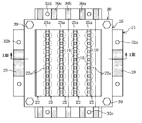
b'ig.12 is a plan view of the solar battery module.
Fig.13 is a cross-sectional view at the line xIII-XIII in Fig.12.
16 Fig.14 is an enlarged plan view of the essential part of the solar hattery
module.
FS.g.15 is a cross-sectional view at the line XV XV in Fig.14.
Fig. 16 is a cross-sectional view at the l.in,e XVI=XVI in F3ig.14.
Fig. 17 is an enlarged view of a part of Fig.15 for explaining behavior.
Fig.18 is an equivalent circuit to the solar battery module.
Fig.19 is an illustrataion equivalent to Fig.13 and showing the solar battery
module according to an modified embodiment.
7
CA 02640083 2008-07-23
Fig,20 is a plan view. of a plate spring member to which multiple solar
battery
celle are fixed in advance in the olax battery module according to the
modified
embodiment.
~ EXPLANATION ON NUMERAI S
I0014]
6 poeitive electrode
6 negative electrode
solar battery cell
-;'
10 20 solar battery module
21 support substrate
22 plate spring member
. ,{
22a ennnertinn flArvp
23 outer frame
24 rubber packing frame
casing plate
25a convex.lena part
25b concave engaging part
26 conductive connection mechanism 20 27 recess
28 positive electrode coating
29 negative electrode coating
= ;õ
8
CA 02640083 2008-07-23
30a, 30b, 80c electrode coating
34 elastic member
BEST MODE FOR IlVIPLEIVIENTINCx THE INVENTION
[0015]
The present invention relates to a light receiving or light emitting
semiconductor module comprising niultiple granular semiconductor elements
having
light receiving or light emitting caapability wherein multiple semiconductor
elements
are individually separable for disposal or repair of the sen4conductor module.
1o EMBODIlI2ENT 1
[001G]
The solar battery module (light receiving semiconductor module) according to
an embodiment will be described hereafter, The structure and production method
of
a spherical silicon aolar battery cell (semiconductor element) will be
described with
reference to Figs. 1 to 7. The structure and production method of this
spherical
silicon solar battery cell is disclosed in the publication of W008/017582 by
the
inventor of the present invention and therefore briefly explained here.
[00171
Fig.1 is a cross-sectional view of a p-type spherical silicon crystal 1
(monocrystal or polycrystal) having a diameter of 1.0 to 2.0 mm. The granular
silicon crystal 1 is produced by melting a eilicon row material in a crucible
at the top
of a drop tube, discharging silicon droplets from the nozzle orifice of the
crucible, and
9
CA 02640083 2008-07-23
allowing them to free-fall in the drop tube having a height of approximately
14 m.
The droplets shaped into a sphere due to surface tension during the fall are
cooled
and eolidified into spherical crystal and recovered at the bottom of the drop
tube.
The silicon crystal 1 of this embodiment is xnonocrystaIline silicon. Those
solidified
at the end of solidifying proceas may have a projection as shown in Fig.1. The
projection is removed and polished to a sphere.
[0018]
As shown in Fig,2, the surface of the spherical silicon crystal 1 is polished
and
partly flattened to form a reference surface 1b, whereby a silicon crystal la
is
obtained. The silicon crystal la has a diameter of approximately 1.8 mm. Then,
as
shown in Fig.3, a ilicon oxide film 2 is formed on the entire surface of the
silicon
crystal la by a known thermal oxidation technique. Then, as shown in Fig.4,
the
silicon oxide film 2 is removed except for a silicon oxide film 2a on the
reference
surface lb and ite vicinity. The silicon oxide film 2a is used as a mask in
the
subsequent impurity diffusion, It is a known technique to leave such a silicon
oxide
fihn in part as a mask.
100191
As shown in Figs. 4 and 5, an n-type impurity is thermally diffused through
the exposed p-type surface lc into the surface part by a known thermal
diffusion
technique using the silicon oxide fil.m 2a as a mask to form an n-type layer
3, thereby
forming a nearly spherical pu junction 3a. Then, the nearly spherical
pnjunction
8a is formed except for the reference surface lb and its vicinity. The silicon
oxide
}
CA 02640083 2008-07-23
film incidentally generated during the thermal diffusion of n-type impurity is
once
removed by a known chemical etching. Then, the silicon crystal la is again
heated
in an oxygen-containing atmosphere to form on the entire surface a silicon
oxide film
4 to a predetermined thickness as shown in Fig.6. The silicon oxide film 4
serves as
G an antireflection coating.
[0020]
Then, a silver=based paste is printed in dots on the flat reference surface lb
(p-type) and on the top (n-type) of the silicon crystal at the opposite
position to the
reference surface lb about the center of the silicon crystal la and processed
at a high
temperature for a short time. Consequently, as shown in Mg.7, the paste
penetrates
the silicon oaÃide film 4 and makes ohmic contact with the p=type silicon
reference
surface lb and the surface of the n-type layer 3 to form a positive electrode
5 and a
negative electrode 6, respectively, whereby a solar battery cell 10 is
obtained. The
positive and negative electrodes 5 and 6 are at opposite positions about the
center of
the silicon crystal la. The center of the silicon crystal la is on the li.ne
connecting
the centers of the positive and negative electrodes 5 and 6.
[00211
The granular and spherical solar battery cell 10 as prepared above has a
spherical pn-junction 3a at a uniform depth below the surface of the silicon
crystal la
and therefore photoelectrically converts incident light in any direction at a
nearly
equal light receiving sensitivity. A spherical light emitting diode having
such a
epherical pn-junction emits uniform light from the spherical surface in any
direction
~~
CA 02640083 2008-07-23
using the electric energy input from the positive electrode 6,
[00221
A solar battery module 20 in which a number of the above described spherical
s4lar battery cells 10 are incorporated and connected in eeries and in
parallel will be
described hereafter with reference to Pigs. 8 to 18.
As shown in Figs. 8 to 12, the solar battery module 20 comprises a support
substrate
21 provided on the under side, a number of solar battery cells 10 arranged in
four
columns on the support substrate 21, five plate spring membere 22 provided in
parallel to the four columns, an outer frame 23, a rubber packing frame 24, a
light
transmissible casing plate 25 on the upper side, a conductive connection
mechanism
26 connecting in parallel multiple (for example eight) solar battery cells 10
in each
column and connecting in series multiple (for example 32) eolar battery cells
10 in
multiple coiumns (for example four), and multiple bolts and nuts 39.
[00231
Fig.8 shows the support substrate 21, thirty two solar battery cells 10
arranged in a matrix of eight rows and four columns on the support substrate
21,
receeees 27 arranged in a matrix of eight rows and four colunans, positive and
negative electrode coatings 28 and 29 and multiple electrode coatings 30a to
30c
formed on the surface of the outer periphery of the support aubetrate 21,
assembly
bolt holes 31, and bolt holes 32a to 32d for connection to conductive
connection plates
(not shown). Fig.9 is a cross-sectional view at the line IX-IX in Fig.8.
[00241
12
CA 02640083 2008-07-23
The conducting direction of the thirty two solar battery cells 10 is aligned
orthogonally to the column direction. In Fig.8, the solar batter,y ceIls 10
each have a
poBitive electrode 6 on the right side in the center and a negative electrode
6 on the
left side in the center (see Figs. 14 and 16). The solar battery module 20 of
this
G embodiment has solar battery cells 10 arranged in a matrix of eight rows and
four
columns for convenience of explanation. In practice, it is constituted by
solar
battery cells 10 arranged in a matrix of several tens or several hundreds rows
and
several tens or several hundreds columns.
[002s]
The support substrate 21 is a white ceramic substrate having a thickness of
approximately 5 mm. It can be a synthetic resin or reinforced glass support
substrate. The support substrate 21 has in the center a cell setup zone 33
where
thirty two recesses 27 are arranged in a matrix of eight rows and four columns
corresponding to the solar battery cells 10 arranged in a matrix of eight rows
and
four columns. The recesses 27 are formed by sandblasting or metal-molding. The
recesses 27 have a nearly semispherical inner surface of revolution (such as
paraboloid of revolution or ellipeoid of revolution) to reflect as much light
as possible
tovvard the solar battery cells 10. The recesses 27 each have a high-
reflectance
silver reflecting fiim 27a on the inner surface.
[0026]
The recesses 27 are frIled with an elastic member 84 (filler) consisting of a
low
adhesive, flexible, and elastic transparent synthetic resin (for example
silicone
is
CA 02640083 2008-07-23
rubber). The elastic member 34 has the top surface below the top surface of
the
eupport substrate 21 by a distance equal to the radius of the solar battery
eells 10.
The positive and negative electrodee 5 and 6 of solar battery ce11s 10 are
exposed near
the top surface of the support eubstrate 21. The thirty two solar battery
cella 10 are
each slightly pressed against the eurface of tbe elastic member 34 and their
position
is secured by the adhesion of the elastic member 34.
[00271
Silver-plated copper printed wirings having a thickness of 0.05 to 0.1 mm are
provided on the support substrate 21 in a frame zone 85 outside the ceIl setup
zone
83. As ehown, in Fig.8, positive and negative electrode coatings 28 and 29
consisting
of copper printed wirings are provided in the right and left parts of the
frame zone 35,
respectively. Three sete of electrode coatings 30a to 30c are provided in the
front
and rear parts of the frame zone 35 and electrically connected to three plate
spring
members 22, respectively. The support substrate 21 has vertical assembly bolt
holes
16 31 in the four corners.
100281 The support substrate 21 has at the right and left ends in Fig.8 serial
connection bolt holes 32a and 32b for coupling conductive connection plates
(not
ahown) to connect in seriee multiple solar battery modules 20 in the
transversal
direction via the positive or negative electrode coating 28 or 29. The support
substrate 21 has at the front- and rear ends in Fig.8 parallel connection bolt
boles 32c
and 32d for coupling conductive connection plates (not shown) to connect in
parallel 14
CA 02640083 2008-07-23
multiple solar battery modules 20 in the longitudinal dixedion via the
electrode
coatings 30a to 30c.
[0029]
Figs. 10 and 11 show the outer frame 23 and rubber packing frame 24. The
outer frame 23 is a square ceramic frame having a thickness of approximately 3
mm
with a square opening 36 corresponding to the cell Aetup zone SS. The outer
frame
23 has a silieone rubber, butyl rubber, or fluoro rubber coating 37 (having a
thickness
of approximately 0.1 to 0.2 mm) on the underside. Abutyl rubber packing frame
24
having a thickneas of approximately 1 mm is placed on the outer frame 23. The
rubber packing frame 24 and outer frarne 23 have assembly bolt holes 38 in the
four
corners. The rubber packing frame 24 and outer frame 23 are superimposed on
the
support substrate 21 and then, five plate spring members 22 are assembled in
the
cell setup zone 33 of the support substrate 21 as shown in Figs. 12 to 16.
[aosol
As shown in Figs. 12 to 16, the plate spring members 22 are made of an elastic
thin metal plate (for example a thin metal plate of beryllium-copper aAoy) in
the form
of an inverted U-shaped crose-section trough. The entire eurface of the plate
spring
members 22 is a high-reflectance light reflecting surface- The plate spring
members
22 have at a pair of free bottom ends connection flanges 22a integrally formed
and
having an extremely narrow horizontal contact surface and an extremely narrow
vertical contact surface, A light reflecting coating can be formed on the
entire
surface of the plate spring members 22 by plating where necessary.
CA 02640083 2008-07-23
[0031a
The plate spring niem,bers 22 have a length larger than the longitudinal
dimension of the cell setup zone 33. The plate spring members 22 stretch
between
the electrode coatings 30a to 30c at the front and rear ends of the cell setup
zone 33.
b Their front ende are connected to one of the front electrode coatings 30a to
30c and
their rear ends are connected to one of the rear electrode coatings 30a to
30c.
[0032)
Before aesembled, the plate spring members 22 have a transversal dimension
(the distance between the vertical contact surfaces of the connection flanges
22e)
slightly smaAer than the distance between the positive and negative electrodes
5 and
6 of two adjacent solar battery cells 10. In this way, when assembled, the
plate
spring members 22 do not press and dislocate the solar battery cells 10.
[0033]
With thirty two solar battery cells 10 being assembled in the thirty two
recesses 27 arranged in a matrix of eight rows and four columne in the cell
setup zone
33 of the support substrate 21, the outer frame 23 is assembled, the rubber
packing
frame 24 having the same shape as the outer frame 23 is assembled on top of
the
outer frame 23, and the five spring plate members 22 are assembled.
[0034)
Three plate spring members 22 among the hive plate spring members 22 are
assembled in the three inter-column spaces of the four columne of solar
battery cells
10. One plate spring member 22 is assembled between the rightmost column of
16
CA 02640083 2008-07-23
eight solar battery cells 10 and the inner surface of the outer frame 23.
Another
plate spring member 22 is asseznbled between the leftmost column of eight
solar
battery cells 10 and the inner surface of the outer frame 23. Eight solar
battery
cells 10 in each column are interposed between the connection flangea 22a of
two
ad,jacent plate spring members 22, whereby the connection flanges 22a are
electrically connected to the corresponding positive or negative electrode 5
or 6. The
front and rear ends in Fig.8 of the plate spring members 22 are in contact
with the
corresponding front and rear electrode coatings 30a to 30c. Then, the light
transmissible casing plate 25 is assembled thereon.
lo [0035]
As shown in Figs. 13 and 15, the casing plate 25 is a colorless transparent
white reinforced glass plate having a thickness of approximately 3 mm. In a
plane
view, the casing plate 26 has the same contour as the outer frame 23. The
casing
plate 25 has bolt holes (not shown) corresponding the bolt holes 31 and 88 in
the four
corners, The casing plate 26 has four rod-shaped convex lens parts 26a
corresponding to the four columns of solar battery cells 10. The convex lens
parts
25a guide light to the respective columns of solar battery cells 10. The
casing plate
has concave engaging parts 25b engaging with the tops of the plate spring
members 22 on the underside at the borders between the convex lens parts 25a.
20 [0036]
Then, the support substrate 21, outer frame 23, rubber packing frame 24, and
casing plate 25 are integrated by inserting bolts 39 in the bolt holes 31 and
38 in the
17
CA 02640083 2008-07-23
..t
four corners and fastening them to nuts (not shown) at the underside.
Meanwhile,
the plate spring members 22 receive a presging force from the concave engaging
parts 25b of the casing plate 25 via compressive deformation of the rubber
packing
frame 24. Therefore, the pairs of connection flanges 22a at the bottom of the
plate
b spring members 22 shift away from each other while keeping contact with the
top
surface of the support substrate 21, electrode coatings 80a to 80c, positive
electrode
coating 28, and negative electrode coating 29. Consequently, the oonnection
flanges
22a make tight contact with the positive or negative electrodes 5 or 6 of the
solar
battery cells 10 in each column, ensuring electrical connection_
to (00371
Fig.18 shows an equivalent circuit to the solar battery module 20 in which
solar battery modules 10 in eight rows and four columns are connected in
series and
in parallel by a mesh-structure circuit. When some solar battery cells 10 are
disabled because of faflure, poor connection, or in shade, there is an
alternative path
bypassing the disabled solar battery cells 10, ensuring external retrieval of
output
from all not-disabled, normal solar battery cells. It is ensured that the
solar battery
module 20 is reliable.
[00s8]
Behavior of the solar battery module 20 will be described hereafter.
20 As shown in Fig.17, light entering the casing plate 25 and convex lens
parts
.25a at a right angle is mainl,y collected by the convex lens parts 25a and
reflected by
the surfaces of the plate spring members 22, then entering the solar battery
cells 10
18
CA 02640083 2008-07-23
for photoelectric conversion. Light passing between the solar battery cells 10
is
diffusely reflected by the inner surfaces of the recesses 27, then entering
the solar
battery cells 10 for photoelectric conversion.
[0039]
On the other haad,: light entering the casing plate 25 and convex lens parts
25
in the centers of the convex lens parts 25a at a right angle enters the solar
battery
cells 10 for photoelectric conversion directly in most part and after
diffusely reflected
by the inner surfaces of the recesses 27 in part. Light transmitted through
the
casing plate 25 is reflected multiple times by the underside of the casing
plate 25,
outer and inner surfaces, of the plate spring members 22, inner surfaces of
the
receesee 27, and surfaces of the solar battery cells 10 before it is absorbed
by the solar
battery cells 10 for photoelectric convereion. In this way, light is
efficiently guided
to the solar battery cells 10 in a closed space, ensuring increased efficiency
and large
output.
is [0040]
The casing plate 25 has the convex lens parts 25a each corregponding to a
column of solar battery cells 10. Therefore, light entering the casing plate
25
obliquely is lees reflected. Reduction in the output according to increase in
the
incident angle of light to the casing plate 25 becomes sma]Ier. Furthermore,
the
plate spring members 22 have a large surface area for their volume, having a
high
heat dissipation capacity. Therefore, the temperature within the solar battery
module 20 does not go up so much and the photoelectric conversion efficiency
of the
.:,
19
CA 02640083 2008-07-23
solar battery cell.s 10 does not go down so much, making the solar battery
module 20
more durable.
I0041]
The above described solar battery module 20 performs the following
advantages.
For disposal of the sdlar battery module 20 after use, four bolts 39 are
removed
to disassemble the support substrate 21, outer frame 23, rubber packing frame
24,
casing plate 25, multiple plate spring members 22, and multiple solar battery
cells 10.
Main components such as solar battery cella 10, plate spring members 22, and
casing
plate 25 can be reused or recycled. Repair of the solar battery module 20 can
easily
and efficiently be done through the same disassemble process.
100421
No soldering is done with the solar battery module 20. No solder connection
process is necessary, no soldering facility is required, and energy for
soldering is
saved. In addition, no thermal fatigue or deterioration at the connection due
to
-soldering is observed,
[0043)
In the solar battery module 20, light collection by the convex lens parts 25a
and light reflection and guiding by multiple plate spring members 22 and
multiple
recesses 27 lead to increase in the amount of light entering the solar battery
oells 10.
Therefore, large output can be obtained using a small number of solar battery
cells
10, sigpificantly reducing production cost of the solar battery module 20. In
a light
CA 02640083 2008-07-23
emitting module in which light emitting diode elements are installed in place
of the
solar battery cells 10, light produced by the light emitting diode elements
can
efficiently be emitted outside in the same manner as above. In such a case,
the
recesses 27 serve to efEciently emit light Qutside.
[00441
The elastic meznbers 34 filling the recesses 27 transmit light and are
effective
in positioning and holding the solar battery cells 10 during the aesembly.
100451
In the solar battery module 20, the internal space storing the solar battery
cells 10 is hermeticall`v sealed from the ambience by the support substrate
21, outer
frame 23, rubber pacldng frame 24, coating 37, and casing plate 25. Therefore,
deterioration of the aolar battery cells 10 due to the ambient air is
prevented and
excellent heat and eound insulation is provided. The support substrate 21 is
made
of ceramic and the casing, plate 25 is raade of reinforced glass. The solar
battery
module 20 has an excellent mechanical strength and high heat and fire
resistance.
The solar battery module 20 has applications as a buildiaag material for
wall.s and
eaves.
[004s1
The solar battery module 20 has the positive and negative electrode coatings
28 and 29 exposed on the outer surface and serial connection bolt holes 32a
and 32b.
Multiple solar battery modules 20 can be arranged in the transversal direction
in
Fig.12 and easily serially connected via not shown conductive connection
plates to
21
CA 02640083 2008-07-23
increase output voltage, Similarly, the solar battery module 20 bas the
electrode
coatings 90a to 80c exposed on the outer surface and parallel connection bolt
holes
32d, Multiple solar battery modules 20 can be arranged in the longitudinal
direction (eolumn direction) in Mg.l2 and easily connected in para]lel via not
shown
conductive connection plates to increase output current.
[00471 Furthermore, the solar battery module 20 has a conductive connection
mechanism 26 connecting multiple solar battery cells 10 in serieg and in
parallel in a
meah structure as shown in Fig,18. When some solar battery cells 10 are
disabled
because of failure, poor connection, or in shade, there is an alternative path
bypassing the disabled solar battery cells 10, ensuring external retrieval of
output
from all not-disabled, normal solar battery cells. It is ensured that the
solar battery
mdule 20 is reliable, [004s]
Partly modified embodiments of the above described solar battery module 30
will be described hereafter.
[11 The support substrate 21 can be constituted by any material easily molded
and allowing for wiring such as polycarbonate (PC), PMMA, glass=cloth based
epoxy
resin, metal enamel, and insulating substrate. It is desirable that the
support
substrate 21 has a light reflecting coating covering the eurfaee entirely or
partly.
The elastic members 34 flling the recesses 27 can be either polyvinyl butyral
or
sthylene vinyl acetate (EVA), which is transparent and adhesive.
22
CA 02640083 2008-07-23
10049] [2] For eaefly serially connecting multiple solar battery modules 20,
for
.,.
example, as shown in Fig.19, the support substrate 21 of the eolar batter
module 20
can have at the right end a down step 21a having a positive electrode coating
28A
6 extended over the top surface and at the left end an up step 21b formed by
removing
the lower half and having a negative electrode coating 29A extended over the
underside.
[00b0]
When multiple solar battery modules 20 are arranged in the transversal
direction in Fig.12 and serially connected, the down atep 21a of the solar
battery
module 20 is overlapped with the up step 21b at the left end of an adjacent
solar
battery module 20 on the right to make the poaitive and negative electrode
coatings
28A and 29A contact with each other. Then, they are electrically serially
connected
by fastening bolts inserted in the series connection bolt holes 32a. Multiple
solar
battery modules 20 can be arranged in the longitudinal direction and connected
in
paraLlel the same manner as above.
[00s1]
[8] The light transmissible casing plate 25 can be constituted by a synthetic
resin that is easy to mold, but not easily broken, such as polycarbonate,
acryl, and
silicone. The convex len.s parts 25a are not essential. They can be omitted so
that
the casing plate 25 has a tlat outer surface.
[4] The height of the plate spring ntembers 22 can be reduced to one half or
one
28
CA 02640083 2008-07-23
phosphor bronze, tungsten steel, nickel eteel, nickel silver, and stainless
eteel.
[0062]
6 [5] As shown in Fig.20, one of the electrodes (for example the negative
electrode in the figure) of multiple solar battery cell8 10 can be fixed to
one
connection flange 22a of a plate spring member 22 by conductive adhesive or
lead-free solder. Then, for assembling the solar battery module 20, the plate
spring
members 22 having the solar battery cells 19 are placed on the top surface of
the
support substrate 21. With this structure, the solar battery module 20 can
significantly easily be assembled.
[0053]
For disposal of the solar battery module 20 having the above structure, the
plate spring members 22 and solar battery cells 10 can be retrieved in the
state as
16 shown in Fig.20 and used as it is. When the solar battery cells 10 should
be
separated from the plate spring members 22, the parts fixed by conductive
adhesive
can easily be separated by a chemical solution and the parts fixed by solder
can
easily be separated by heating.
[0054]
[6]The outer frame 23 can be made of glass-cloth based epoxy resin or
polycarbonate. The rubber packing frame 24 can be made of silicone rubber or
fluoro rubber.
24
CA 02640083 2008-07-23
[7] Solar battery cells or light emitting diode elements consisting of a
epherica.l
core having a thin semiconductor layer formed on the surface to create a pn-
junction
as set forth in the publication of W099/10935 can be used in place of the
above
described spherical solar battery cells 10. The module in which multiple light
6 emitting diode elements are installed in place of the above described
multiple solar battery cells is a plane emission light emitting module.
[00551
[8] The above described embodiments are given by way of example. The
present invention can be realized by a person of ordinary skill in the art by
partially
modifying the above described embodiments without departing from the scope of
the
present invention.
INDUSTRJAL APPLICABILITY
[00561
16 The light receiving or light emitting semiconductor module of the present
invention is effectively used in solar battery panels or light emitting
panels.