Note: Descriptions are shown in the official language in which they were submitted.
CA 02640468 2008-10-06
Title Of The Invention
Touch switch for electrical appliances and electrical appliance provided with
such
switch
This application claims priority from, and incorporates that contents of,
European
Patent Application 07118016.0 filed October 8, 2007.
Background And Field Of The Invention
The.present invention relates to a touch switch for an electrical appliance to
be
used on control panels thereof. The invention particularly refers to a
capacitive
touch switch comprising a capacitive flat sensor surface, a light source, a
transparent cover provided over said touch switch and a printed circuit board
connected to said capacitive sensor element.
With the term "switch" we mean every kind of touch sensors which usually
replace the traditional buttons in modern flush user interfaces.
Visual feedback activation of a touch switch control is simply provided by a
light
source, for example a light emifting diode (LED)., Usually several touch
switches
are arranged, together with control board thereof, in a control panel.
To avoid optical interference between adjacent touch switches, light flux
shall be
conveyed from a light source to the related touch sensitive switch surfaces.
Opaque walls or light guide means are normally provided for this object. The
use
of opaque walls increases physical dimensions and renders the mounting quite
complex.
CA 02640468 2008-10-06
Light guides can be used as mechanical support for the electrodes. Electrodes
can also be made of transparent conductive material (such as indium tin
oxide),
located between the light guide and the lower surface of the transparent cover
under which the touch switch is placed, with an increase of the overall cost
of the
control panel.
On top of the above illumination problems, there is the need of assuring a
good
mechanical connection between the touch switch and the transparent cover
(usually a glass or plastic plate) under which the switch is placed. Up to
now, for
assuring such mechanical contact springs or conductive rubber elements have
been used, which may increase the overall cost and complex.ity of the single
touch switch, particularly as far as the need of assuring a good electrical
contact
of the springs is concerned. Moreover, technical solutions are known (for
instance from US-A-2006/0243575) in which a support member, carrying
electronic components, is separated from the transparent cover by a series of
opaque septum-like partitions for creating physically delimited illumination
channels. Even if such solution does not require light guides (light emitting
diodes are placed on the support member directly), nevertheless it is quite
bulky
and of complex manufacturing.
It is an object of the present invention to propose a different structural
arrangement of a touch switch in order to allow a reduction of physical
dimensions of the switch, easy mounting process, and improvement on
versatility
for different symbols as painted objects.
Another object of the present invention is to provide a touch switch that has
an
improved sensibility.
2
CA 02640468 2008-10-06
A further object of the present invention is to provide a capacitive touch
switch
without an external icon serigraphy and which, when not activated or not in
use
(when the control panel is off) is not visible by the user.
A further object of the present invention is to provide a touch switch that
can give
a direct feedback to the user when a command has been duly received.
A further object of the present invention is to provide a touch switch that is
substantially invisible by the user, its presence being detected only when the
user's finger touches an enabling switch.
The invention is also focused on a touch switch of the above type in which the
light source includes an illuminated display.
A capacitive touch sensor of this specific type is disclosed by US-A-6403904
in
which a housing of a seven-segment display is soldered to with soldering pins
to
the printed circuit board detached from the transparent cover. The capacitive
flat
sensor surface in contact with the transparent cover has a frame-shaped flat
portion around the seven-display housing and is connected to the printed
circuit
board by means of standing legs. This technical solution is quite bulky, due
to the
thickness of the standard seven-segment display package. Moreover it needs a
precise mounting for assuring a correct contact of the capacitive flat sensor
surface against the transparent cover. In order to overcome this problem,
known
touch switches make use of actuators or conductive elements (springs, sponges,
rubbers, etc... ) for the electrical contact and the mechanical arrangement
between touch area and touch sensor.
Another disadvantage of the above known solution is that the capacitive
surface
is obtained starting from a metal sheet from which are punched or worked the
3
CA 02640468 2008-10-06
central cut-out and notches, which leads to an increase of the overall cost of
the
touch switch.
Another known possibility is the use of a printed circuit board (PCB) having a
bigger thickness, for example 4 mm, to avoid the use of actuators or
conductive
elements. The use of such thick PCB increases the overall cost of the touch
switch, and moreover it can create problem of differential thermal expansion
particularly when the touch switch is used in cooking appliances (cooking
hobs,
ovens) where the temperature of the switch can reach values closer to 100 C or
above.
It is a further object of the present invention to provide a capacitive touch
switch
with an illuminated display that does not present the above problems and that
has a reduced cost.
According to the invention, the above objects are obtained thanks to the
features
listed in the appended claims.
According to the present invention, no leg is needed to cover the gap between
touch area and sensor surface due to light source or display package.
Moreover there is no need to use PCB having a big thickness, for example 4 mm
or above, or multilayered PCB to cover gap between touch area and touching
sensor due to display package.
Brief Description Of The Drawings
Further features and advantages of a touch switch according to the present
invention will become clear from the, detailed description provided as a non
limiting example, with reference to the attached drawing in which:
4
CA 02640468 2008-10-06
- figure 1 shows a cross section of a touch switch according to a first
embodiment of the present invention;
- figure 2 is a top view of a component of the touch switch of figure 1;
- figure 3 is a view from the bottom of another component (PCB) of the
touch switch of figure 1;
- figure 4 shows a cross section of a touch switch according to a second
embodiment of the present invention;
- figure 5 shows a cross section of a touch switch according to a third
embodiment of the present invention;
- figure 6 is a perspective view of a seven-segment display used in the
embodiment of figure 5,
- figure 7 shows a cross section of a touch switch according to a fourth
embodiment of the present invention; and
- figure 8 shows a cross section of a touch switch according to a fifth
embodiment of the present invention.
Description Of A Preferred Embodiment
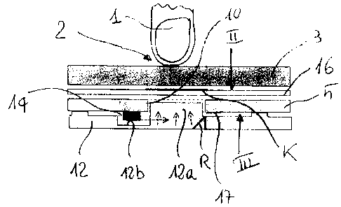
With reference to the drawings, a touch switch presents a non-conductive
transparent cover 3, for instance of glass or polymeric material. On the
transparent cover 3 there is at least one touch sensitive area 2 adapted to be
touched by the user's finger 1. On the lower face of the transparent cover 3,
a
single side printed circuit board (PCB) 5 is attached by means of a non-
conductive transparent adhesive 4 (figure 5). The PCB 5 is provided with a cut-
out 10.
With reference to figure 1, on the side of-the PCB 5 opposite the transparent
cover 3 (i.e. the side with the metallic tracks), there is provided a plastic
light
guide 12 in the form of a planar sheet provided with a protrusion 12a located
in
the cut-out 10 of the PCB. The light guide 12 is fixed to the PCB 5 by means
of
CA 02640468 2008-10-06
adhesive or the like, and adjacent the protrusion 12a the light guide 12
presents
a seat 12b in which a LED 14, electrically connected to and supported by the
PCB 5, is placed. In the area surrounding the cut-out 10, the PCB 5 presents
an
annular track 17 which acts as a touch electrode and is interrupted in
correspondence of the LED 14 (figure 3). Between the transparent cover 3 and
the PCB 5 a polymeric film 16 is interposed, that has the function of a light
filter.
The film 16 is substantially opaque and presents circular transparent zones
16a
where icons K are obtained by printed serigraphy. When the LED 14 is switched
on, light is guided in the protrusion 12a, possibly with the help of
reflective
portions R inside the light guide 12. Therefore light emerges from the
protrusion
126 and is filtered by the film 16, displaying the respective icon K as shown
in
figure 2. The level of illumination may be linked to the electrical state of
the touch
switch. For instance, when the appliance is switched on all the icons K can be
illuminated at a first identical level in order to allow the user choosing
among
them. When the user touches a switch, the level of illumination of that single
switch is automatically increased to a second higher level in order to give
the
user an immediate feedback. The use of the film 16 improves the flexibility of
use
of the user interface. For example, by just changing this layer it is possible
to
easily customize the user interface for different countries and languages.
When a
big light diffusion effect is requested, the film 16 can be thicker (few
millimetres)
with "ad hoc" treated surfaces; otherwise this film can be very thin or it can
be
removed when the serigraphy is printed directly on the transparent cover 3.
Even if in the example of figures 1 to 3 the touch electrode 17 is realized as
a
circular crown with a hole in the centre for the light guide, other shapes can
be
easily adopted.
The embodiment according to figure 4 differs from the previous one because no
light guide is needed. In figure 4 parts which are identical or similar to the
parts of
the previous embodiment are indicated with the same reference numerals. On a
face of the PCB 5 opposite the transparent cover 3 a body package 9 of a
6
CA 02640468 2008-10-06
reversed mounted LED is soldered around the cut-out 10 by means of metal
pins. Also in this case the touch electrode 17 is realized as a circular
crown.
In the embodiment shown in figures 5 and 6, the body package around the cut-
out 10 is a seven-segment display 9' which is soldered by means of metal pins
8.
On the same surface of the PCB 5 there are provided two electrodes 6 that, for
examples, can be used for increasing (+) or decreasing (-) a certain
parameter.
The mounting of the seven-segment display 9' is very easy. A low cost single
side PCB 5 with standard thickness as FR4 or CEM1 type can be used. No
conductive elements like spring or sponges or conductive rubber have to be
used. An air gap between the seven-segment display 9' and transparent cover
assures better performances in hot applications like cooktops or oven.
Moreover,
when the display is switched off, it is not seen by the user (dark effect on
surface
when off). A further advantage of using a display as the one shown in figure 6
relates to the possibility of using a display whose thickness may be different
from
the thickness of the PCB. As a matter of fact in the standard known solution
the
thickness of the display must be identical to the thickness of the PCB, and
the
soldering part of the display must be flush with the surface of the PCB. This
is no
longer needed with a display according to the present invention.
Another embodiment is shown in figure 7, which is quite similar to the
embodiment according to figures 1 to 3 but it can be used also when the
transparent cover 3 is not flat. In this embodiment the protrusion 12a of the
light
guide 12 is not substantially flush with the PCB 5, rather it goes beyond the
plane
of the PCB towards the transparent cover 3 that, in this case, is detached
from
the PCB. For assuring a proper working of the touch switch, a metal spring 20
is
interposed between the PCB 5 and the film 16 carrying the icons serigraphy K
and in contact with the transparent cover 3. The spring 20 has an enlarged end
20a sandwiched between the PCB (on the circular track 17) and the light guide
12.
7
CA 02640468 2008-10-06
The embodiment according to figure 7 provides the following functionality and
advantages. The more large part 20a of the spring 20 compressed between the
PCB and the plastic light guide or support provides a good electrical contact
between the touch electrodes 17 (contacts) and the spring. This arrangement
avoids the cost for a double side PCB and for a welding process of the spring.
To
avoid the welding process allows using a cheaper material for the spring 20
(no
tinned steel is required). The other end of the spring 20 is pressed on upper
layers (user interface surface and light filter and serigraphy), providing the
electrical continuity of the touch sensor closed to the user interface surface
(avoiding the air gap between touch sensor and user interface surface). The
touch performance is improved if more spring coils when pressed are closed to
the user interface surface, because this improves the surface of the capacitor
plate of the sensor.
A further embodiment similar to the previous one is shown in figure 8 where
the
spring 20' does not have any enlarged end and it is interposed between the PCB
and the transparent cover 3(with the optional interposition of the plastic
film 16
with serigraph). In this solution the touch sensors/electrodes 17' are
realized on
PCB in the opposite side where LED 14 is placed.
8