Note: Descriptions are shown in the official language in which they were submitted.
CA 02641810 2008-08-07
SPECIFICATION
"ELECTRONIC APPARATUS WITH PROTECTIVE PANEL"
Technical Field
The present invention relates to an electronic apparatus with a protective
panel, wherein an enclosure mounting a display device therein forms a display
window for exposing a display section of the display device to the outside,
the
display window includes a support portion for supporting the protective panel
for
the display device, with the protective panel being fitted within the display
window.
Background Art
Conventionally, in the case of an electronic apparatus with a protective
panel described above, the enclosure mounting the display device therein forms
a
recess. In a bottom face of this recess of the enclosure, there is defined an
aperture for exposing the display section of the display device to the
outside. The
protective panel for the display device is fitted within the recess, in such a
manner
that the peripheral edge portion of the protective panel is supported directly
to the
peripheral edge of the bottom face of the recess (see, e.g. Patent Document
1).
Patent Document 1: W02005/064451 (paragraphs 0042 through 0043,
Figs. 3-4).
Disclosure of the Invention
Problem To Be Solved by Invention
In recent years, some of mobile phones or "smart" phones as an example of
an electronic apparatus with a protective panel, are provided with multiple
functions, i.e. not only the main telephoning function, but also other
functions
such as an electronic mailing function, internet function, as well as such
additional functions as photographing function and music playing function. In
order to achieve such increasing of functions while avoiding enlargement of
the
electronic apparatus, it is desired that each switch should be configured to
serve
-1-
CA 02641810 2008-08-07
for multiple of purposes, thereby reducing the total number of switches to be
additionally provided.
However, if such multi-purpose configuration of switches goes to extreme,
each switch is provided with too many functions, which invites deterioration
in the
operational ease and efficiency. Further, as there practically exits a limit
in the
number of the switches provided for achieving the original functions and in
the
number of the switches additionally provided, further increase in the
functions of
the electronic apparatus will necessarily invite enlargement of this
electronic
apparatus.
The object of the present invention is to enable further increase in the
functions of the electronic apparatus while avoiding or restricting
enlargement of
the electronic apparatus or deterioration in the operational ease and
efficiency,
through effective utilization of the protective panel which is included
originally in
the electronic apparatus with a protective panel, or to achieve improvement in
the
operational ease and efficiency while avoiding or restricting enlargement of
the
electronic apparatus.
Means To Solve Problem
For accomplishing the above-noted object, according to a characterizing
construction of an electronic apparatus with a protective panel relating to
the
present invention, the electronic apparatus comprises:
a display device having a display section;
an enclosure having a display window which is open in one direction and
mounts therein said display device so as to expose said display section to the
outside;
a protective panel disposed at said display window so as to cover said
display section from the outside; and
a pressure-sensitive conductive rubber interposed between a movable
portion including at least said protective panel of said protective panel and
said
display device and a frame-like support portion defined by a surface of said
enclosure within said display window, so as to prevent intrusion of foreign
substance to the interior of said enclosure through said display window, said
rubber detecting a depressing operation on said movable portion.
With the above-described characterizing construction, there can be
obtained a pressure-sensitive sensor comprised of the protective panel as an
-2-
CA 02641810 2008-08-07
operational portion and the pressure-sensitive conductive rubber as a
pressure-sensitive element. And, this pressure-sensitive sensor can be used as
a
switch to which a function of a switch to be newly added to the electronic
apparatus or a function of an existing switch included originally in the
electronic
apparatus is assigned.
Further, if this pressure-sensitive sensor utilizing the movable portion
including at least the protective panel is used as a switch corresponding to a
function to be newly added to the electronic apparatus, it is possible to
eliminate
space which would otherwise be required for disposing a switch dedicated to
that
function. Or, it is possible to avoid assigning that new function to an
existing
switch, which assignment would be required in case the existing switch is
configured to additionally provide that new function. As a result, it becomes
possible to enable further increase in the functions of the electronic
apparatus
while avoiding or restricting enlargement of the electronic apparatus in case
space
is secured for an additional switch dedicated to a further function or
deterioration
in the operational readiness and efficiency resulting from causing an existing
switch to function as a switch corresponding to a new function.
Further, if this pressure-sensitive sensor utilizing the movable portion is
used as a switch to which a function assigned previously to an existing switch
is
assigned, it is possible to eliminate a space for disposing the switch
dedicated to
that function, which space would otherwise be required for newly disposing
such
dedicated switch to which the function is assigned. As a result, it is
possible to
improve the operational readiness and efficiency, while avoiding or
restriction
enlargement of the electronic apparatus which would occur otherwise in order
to
ensure a switch disposing space.
And, the protective panel is provided for the purpose of protecting the
display device. Hence, if arrangement is made such that the function of the
pressure-sensitive sensor utilizing the movable portion having this protective
panel may vary in accordance with displayed contents of the display section, a
user can operate the pressure-sensitive sensor without difficulty or
confusion, even
when such many functions are assigned to this pressure-sensitive sensor.
Moreover, with the pressure-sensitive conductive rubber, it is possible to
prevent intrusion of foreign substances such as water, dust, etc. through the
display window to the interior of the enclosure, without providing any sealing
member dedicated to such purpose. As a result, it is possible to avoid
deterioration and short circuit of cable connections or deterioration of the
display
-3-
CA 02641810 2008-08-07
device or substrate, due to intrusion of such foreign substances through the
display window.
Furthermore, if an analog type whose conductivity varies according to the
magnitude of external force is employed as the pressure-sensitive conductive
rubber, it becomes possible to construct a variable type pressure-sensitive
sensor
which provides a resistance value variable according to the magnitude of the
external force applied to the movable portion. With this, in the case of an
electronic apparatus having a photographing function, the pressure-sensitive
sensor can be used as a zoom switch for varying the zooming speed according to
the magnitude of the external force applied to the movable portion or a
shutter
switch for varying the shutter speed according to the same. Further, in the
case
of an electronic apparatus having an image drawing function, the
pressure-sensitive sensor can be utilized as a drawing pressure sensor for
varying
the image density according to the magnitude of the external force applied to
the
movable portion.
Therefore, by interposing a pressure-sensitive conductive rubber between
the movable portion and the support portion, thereby constructing a
pressure-sensitive sensor effectively utilizing the protective panel included
in that
movable portion, it becomes possible not only to achieve further increase in
the
number of functions of the electronic apparatus while avoiding or restricting
enlargement of the electronic apparatus or deterioration in the operational
readiness and efficiency, but also to achieve high reliability due to enhanced
water-proof performance and dust-proof performances.
According to a further characterizing construction of an electronic
apparatus with a protective panel relating to the present invention, the
distance
between the movable portion and the support portion where the pressure-
sensitive
conductive rubber is interposed, decreases in response to an increase in the
magnitude of a depressing force by the depressing operation.
With the above-described characterizing construction, in accordance with
increase of the depressing force by the depressing operation to the movable
portion,
the pressure-sensitive conductive rubber becomes compressed to provide a
correspondingly smaller electric resistance. As a result, when the electric
resistance of the pressure-sensitive conductive rubber becomes equal to or
smaller
than a predetermined threshold value, this can be determined as occurrence of
a
depressing operation to the movable portion.
According to a still further characterizing construction of an electronic
-4-
CA 02641810 2008-08-07
apparatus with a protective panel relating to the present invention, the
distance
between the movable portion and the support portion where the pressure-
sensitive
conductive rubber is interposed, increases in response to an increase in the
magnitude of a depressing force by the depressing operation.
With the above-described characterizing construction, in accordance with
increase of the depressing force by the depressing operation to the movable
portion,
the pressure-sensitive conductive rubber becomes expanded to provide a
correspondingly greater electric resistance. As a result, when the electric
resistance of the pressure-sensitive conductive rubber becomes equal to or
greater
than a predetermined threshold value, this can be determined as occurrence of
a
depressing operation to the movable portion.
According to a still further characterizing construction of an electronic
apparatus with a protective panel relating to the present invention, one of
the
movable portion and the support portion which comes into contact with the
pressure -sensitive conductive rubber or the pressure-sensitive conductive
rubber
is configured such that a cross-sectional area thereof normal to an applying
direction of the depressing force by the depressing operation varies
continuously or
stepwise along the applying direction of the depressing force.
In the case of a pressure-sensitive conductive rubber whose cross-sectional
area does not vary along the applying direction of the depressing force, e.g.
in the
case of a pressure-sensitive conductive rubber which is shaped rectangular,
the
resistance value of the pressure-sensitive conductive rubber will vary sharply
from
the initial stage of application of the input load, and will hardly vary
according to
variation in the input load at the $nal stage of the application of the input
load.
For this reason, although detection of presence/absence of a depressing
operation
based on a variation in the resistance value is possible at the initial stage
of
application of the input load, but the detection is difficult at the final
stage of the
application of the input load.
On the other hand, according to the above-described characterizing
construction, at the initial stage of application of the input load, the
contact area
between the pressure-sensitive conductive rubber and the support portion or
the
movable portion of the enclosure is small and then this contact area
progressively
increases toward the final stage of application of the input load. Therefore,
at the
initial stage of application of the input load, there occurs no such sharp
change in
the resistance value of the pressure-sensitive conductive rubber in accordance
with variation in the input load. And, at the initial stage of application of
the
-5-
CA 02641810 2008-08-07
input load too, in association with increase in the contact area, the
resistance
value of the pressure-sensitive conductive rubber will vary according to
variation
in the input load. Accordingly, the condition of the depressing force (input
load)
due to a depressing operation can be determined in a reliable manner, in
accordance with variation in the resistance value of the pressure-sensitive
conductive rubber from the initial stage to the final stage of application of
the
input load.
According to a still further characterizing construction of an electronic
apparatus with a protective panel relating to the present invention, at a
portion of
the protective panel to be subjected to a depressing force of a depressing
operation,
there is provided a reinforcing structure member for enhancing the rigidity of
the
protective panel.
With the above-described characterizing construction, with the provision
of this reinforcing structure member, the rigidity of the protective panel
against
the depressing operation is enhanced, thus reducing e.g. flexion of the
protective
panel. As a result, the depressing force due to a depressing operation can be
transmitted reliably to the pressure-sensitive conductive rubber, whereby the
depressing operation can be detected reliably also.
According to a still further characterizing construction of an electronic
apparatus with a protective panel relating to the present invention, the
pressure-sensitive conductive rubber is formed like a loop along the support
portion.
With the above-described characterizing construction, the
pressure-sensitive conductive rubber is to be disposed along the peripheral
edge of
the back face of the movable portion supported by the support portion. And,
when a depressing operation is effected on the protective panel included in
the
movable portion, regardless of the position of this depressing operation, the
pressure to the protective panel will be transmitted to the pressure-sensitive
conductive rubber, thereby rendering this pressure-sensitive conductive rubber
conductive. Accordingly, the depressing operation to the protective panel can
be
detected in an even more stable and reliable manner.
Further, with the pressure-sensitive conductive rubber, the gap between
the back face peripheral edge of the movable portion and the support portion
can
be reliably sealed without any interruption. As a result, intrusion of foreign
substance through the display window to the interior of the enclosure can be
prevented reliably, and deterioration and/or short circuit of the cable
connections
-6-
CA 02641810 2008-08-07
due to the intrusion of foreign substance through the display window can be
avoided in a reliable manner.
Therefore, it is possible to obtain a pressure-sensitive sensor having
further improved detection performance, and to enhance also its water-proof
performance, dust-proof performance, etc.
According to a still further characterizing construction of an electronic
apparatus with a protective panel relating to the present invention, the
pressure-sensitive conductive rubber includes a connector extending from an
inner
wall of the rubber toward the interior of the enclosure.
With the above-described characterizing construction, it becomes possible
to provide the wiring to the pressure-sensitive conductive rubber on the inner
side
(the side of display window) of the pressure-sensitive conductive rubber where
intrusion of foreign substance is prevented by the pressure-sensitive
conductive
rubber. Hence, it becomes possible to avoid the deterioration or short-circuit
of
cable connections due to intrusion of foreign substance to the wiring portion,
without providing any special sealing member dedicated thereto.
Accordingly, it becomes possible to provide the apparatus with further
improved water-proof performance and dust-proof performance, without inviting
complexity of its construction.
According to a stiIl further characterizing construction of an electronic
apparatus with a protective panel relating to the present invention, on one
face of
the pressure-sensitive conductive rubber, there is mounted a pair of
combtooth-like electrodes, via which a depressing operation to the movable
portion
is detected.
With the above-described characterizing construction, the construction
requires provision of the combtooth-like electrodes only on one face of the
pressure-sensitive conductive rubber. Hence, this facilitates mounting of the
electrodes to the pressure-sensitive conductive rubber. Further, as this
construction allows the gap between the pair of electrodes to be small,
resistance
variation in the pressure-sensitive conductive rubber can be detected with
high
sensitivity. And, in doing this, there is no necessity of changing the
thickness of
the pressure-sensitive conductive rubber, so it is possible to ensure a
sufficient
depressing margin for the depressing operation on the protective panel
(movable
portion).
According to a still further characterizing construction of an electronic
apparatus with a protective panel relating to the present invention, one or
both of
-7-
CA 02641810 2008-08-07
the movable portion and the support portion defines or define a groove for
receiving the pressure-sensitive conductive rubber therein.
With the above-described characterizing construction, it is possible to
effect the attachment of the pressure-sensitive conductive rubber at an
appropriate position relative to the movable portion or the support portion,
in an
easy and reliable manner. This allows improvement in the assembly readiness,
also prevention of deterioration in the detection performance as well as in
the
water-proof performance and/or dust-proof performance, due to inadvertent
displacement of the pressure-sensitive conductive rubber from its proper
position.
The above construction also allows increase in the sealing condition between
the
movable portion or the support portion and the pressure-sensitive conductive
rubber, which increase further improves the water-proof and dust-proof
performances.
Accordingly, it becomes possible to increase the reliability with ensuring
the superior detection performance as well as the water-proof performance and
dust-proof performance, while improving the assembly readiness also.
According to a still further characterizing construction of an electronic
apparatus with a protective panel relating to the present invention, said
protective
panel is configured to provide functions as a touch panel.
With the above-described characterizing construction, it becomes possible
to obtain a pressure-sensitive sensor with a touch-panel function, utilizing a
protective panel, capable of detecting a depressing operation to the
protective
panel and detecting also the position of the depressing operation on the
protective
panel. And, the sensor can be used as a multiple-function switch capable of
providing a great variety of complicated functions or a tablet with a drawing
pressure detecting function, through combinations of the pressure information
and
the position information.
And, in case the panel is used as a multiple-function switch, the panel can
be configured such that the relationship between the depressing operation
position
and the function corresponding thereto may be displayed at a displaying area
of
the display section corresponding to that depressing operation position. With
this,
an operation corresponding to a function can be carried out without difficulty
or
confusion.
Incidentally, referring to some possible examples of using as a
multiple-function switch, in the case of an electronic apparatus having a
photographing function for example, the construction can be adapted to
function
-8-
CA 02641810 2008-08-07
as a zoom switch or a shutter switch, in accordance with a depressing
operation
position on the protective panel. In the case of an electronic apparatus
having a
navigating function, it can be adapted to function as a destination
registering
switch which determines a destination according to the depressing operation
position on the protective panel and then determines presence/absence of
registration of the location based on the depressing force applied at that
depressing operation position.
Therefore, with the provision of the touch panel function to the protective
panel, the pressure-sensitive sensor utilizing the movable portion including
this
protective panel can, by itself, be configured to provide a greater number of
functions. With this, it becomes possible to provide the electronic apparatus
with
further increased functions without inviting enlargement of the electronic
apparatus or deterioration in the operational efficiency or to form the
apparatus
compact, without inviting deterioration in the operational readiness or
efficiency.
Best Mode of Embodying the Invention
[First Embodiment]
Next, a first embodiment of the present invention will be described with
reference to the accompanying drawings.
Some non-limiting examples of the electronic apparatus with a protective
panel relating to the present invention are a mobile phone, a "smart" phone, a
PDA, a car navigation apparatus, a digital camera, a digital video camera, a
game
machine, and a tablet. In this, a cell phone 1 will be explained as one
example.
Fig. 1 is a perspective view of the cell phone 1. Fig. 2 is a cross sectional
view taken along a line II-II in Fig. 1, of principal portions, showing a
construction
of a protective panel according to the first embodiment, Fig. 3 is an exploded
perspective view showing the construction of the protective panel according to
the
first embodiment.
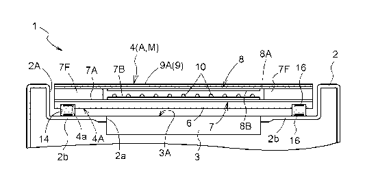
As shown in Figs. 1-3, in this mobile phone 1 as an example of an
electronic apparatus with a protective panel, includes an enclosure 2 made of
a
synthetic resin forming a display window 2A in its front face, the enclosure 2
mounting therein a display deice 3 having a display section 3A made of liquid
crystal or organic EL, etc., a protective panel 4 for protecting the surface
of the
display device 3, and a plurality of input keys 5, etc.
-9-
CA 02641810 2008-08-07
The display window 2A of the enclosure 2 is formed concave with a
stepped portion to allow fitting of the protective panel 4 therein. And, the
display
window 2A is open in its bottom face, with an aperture portion 2a for exposing
the
display section 3A of the display device 3 mounted within the enclosure 2 to
the
outside and a frame-li.ke support portion 2b for supporting a back face
peripheral
edge 4A of the protective panel 4.
The shape and size of the display window 2A can vary, depending on the
shape and size of the protective panel 4. Further, the concavity depth of the
display window 2A can also vary depending on e.g. the thickness of the
protective
panel 4. Moreover, the shape and size of the aperture portion 2a of the
display
window 2A can vary, depending on the shape and size of the display section 3A.
In this embodiment, the display window 2A, the aperture portion 2a, the
display
section 3A and the protective panel 4 are formed rectangular or approximately
rectangular, and the concavity depth of the display window 2A is set to render
the
surface of the enclosure 2 and the surface of the protective panel 4 disposed
in a
same level.
The protective panel 4 can be configured selectively as either one having
the so-called touch input function for detecting X-Y coordinates of an
operated
position of a touch operation on the protective panel 4, or one not having
such
touch input function. And, the touch-input type panel can be selectively
configured as one of a resistor-film type, a capacitance type, an electro-
magnetic
induction type, etc. In this embodiment, one comprising a resistor-film, touch
input function will be explained as an example.
As shown in Fig. 2 and Fig. 3, the protective panel 4 includes a support
plate 6 formed of a resin having superior transparency, rigidity, and
workability, a
lower electrode film 7 affixed to the upper face of the support plate 6, an
upper
electrode film 8 disposed in upward opposition to the lower electrode film. 7
via an
air layer, a design sheet 9 affixed to the upper face of the upper electrode
film 8,
etc., so that the panel is configured as one having the resistor-film type
touch
panel function.
As the resin used for the support plate 6, selection is possible from among
those having superior transparency, rigidity and workability, such as
polycarbonate resin (PC), methacrylic resin (PMMA), acrylonitrile -styrene
copolymer resin (AS), acrylonitrile-butadiene-styrene copolymer resin (ABS),
cellulose-propionate (CP), polystyrene (PS), polyester resin, and polyethylene
resin
(PE), and it is preferred to employ polycarbonate resin (PC) or methacrylic
resin
-10-
CA 02641810 2008-08-07
(PMMA.) having especially good transparency.
Also, the thickness of the support plate 6 can be selected from the range of
0.5 to 3.0 mm. In particular, 1.0 mm is preferred.
Fig. 4 is a plan view of the lower electrode film, and Fig. 5 is a bottom view
of the upper electrode film, respectively.
As shown in Figs. 2-4, the lower electrode film 7 is formed by forming, on
the upper face of a transparent insulating substrate 7A, a rectangular
transparent
conductive film 7B, a pair of parallel lower bus bars 7C disposed along the
two
opposed sides of the transparent conductive film 7B, a pair of lead circuits
7D
disposed along the perimeter of the transparent conductive film 7B, a pair of
relaying electrodes 7E, and a frame-like bonding layer 7F.
As shown in Figs. 2, 3 and 5, the upper electrode film 8 is formed by
forming, on a lower face of a flexible transparent insulating substrate 8A
having
flexibility to be flexed when e.g. being depressed with a finger, a
rectangular
transparent conductive film 8B, a pair of parallel upper bus bars 8C disposed
along the two opposed sides of the transparent conductive film 8B, and a pair
of
lead circuits 8D and a pair of relaying electrodes 8E disposed along the
perimeter
of the transparent conductive film 8B.
The transparent insulating substrate 7A of the lower electrode film 7 and
the flexible transparent insulating substrate 8A of the upper electrode film 8
can
be formed of an engineering plastics such as polycarbonate, polyamide,
polyetherketone type or a transparent film of acryl, polyethylene
terephthalate,
polybutylene terephthalate, etc.
The transparent conductive films 7B, 8B of the lower electrode film 7 and
the upper electrode film 8 can be formed of a metal oxide film of tin oxide,
indium
oxide, antimony oxide, zinc oxide, cadmium oxide, indium tin oxide (ITO), etc.
a
composite film containing such metal oxide as above as the principal
component,
or a metal film of gold, silver, copper, tin, nickel, aluminum, paradigm, etc.
Further, the transparent conductive films 7B, 8B can be multiple-layer
construction comprised of two or more layers.
Some non-limiting examples of the method of forming the transparent
conductive films 7B, 8B include vacuum deposition method, sputtering method,
ion-plating method, CVD method, etc.
As shown in Figs. 2 through 4, on a surface of one of the transparent
conductive films 7B, 8B, there can be formed a plurality of fine-dot-like
spacers 10
for preventing erroneous contact between these transparent conductive films
7B,
-11-
CA 02641810 2008-08-07
8B when these are placed in opposition to each other.
The spacers 10 can be formed of a transparent light-curing resin such as
epoxy acrylate type or urethane acrylate type, or a transparent heat-curing
type
resin of polyester type or epoxy type. Further, some non-limiting examples of
the
method of forming the spacers 10 include a printing method such as screen
printing technique or photo processing technique.
The lower bus bars 7C, the upper bus bars 8C, the lead circuits 7D, 8D and
the relaying electrodes 7E, 8E can be formed by using a conductive paste of a
metal such as gold, silver, copper, nickel, etc. or carbon. Some non-limiting
examples of the method of forming these include printing methods such as
screen
printing method, offset printing method, gravure printing method, flexographic
printing method, the photo resist method, and brush applying method.
In general, the lower bus bars 7C and the upper bus bars 8C are formed
such that these are formed as closely as possible to the ends of the
transparent
insulating substrate 7A or the flexible transparent insulating substrate 8A,
so as
to ensure, at the center portion of the transparent insulating substrate 7A or
the
flexible transparent insulating substrate 8A, as large as possible an area
where
these lower bus bars 7C or the upper bus bars 8C are not formed.
The size and the shape of the area where the lower bus bars 7C or the
upper bus bars 8C are not formed, that is, the input area or the display area,
can
be variably set, depending on the size and the shape of the input area or the
display area of the electronic apparatus with a protective panel such as the
cell
phone 1. .
As shown in Fig. 2 and Fig. 3, the design sheet 9 is formed by forming a
hard-coat layer on the upper face of the flexible transparent insulating
substrate
9A and forming a picture design layer and a bonding layer on the lower face of
the
same.
The flexible transparent insulating substrate 9A of the design sheet 9 can
be formed of an engineering plastics such as polycarbonate, polyamide,
polyether-ketone type or a transparent film of acryl, polyethylene
terephthalate,
polybutylene terephthalate, etc.
The thickness of the flexible transparent insulating substrate 9A can be
selected from the range from 50 to 200 g m, preferably from the range from 100
to
125,u m.
The material used for the hard-coat layer of the design sheet 9 can be an
inorganic material such as siloxane type resin, acrylic epoxy type resin or an
-12-
CA 02641810 2008-08-07
organic material such as urethane type heat-curing type resin or acrylate type
light-curing resin. The thickness of the hard-coat layer ranges appropriately
from
1to7 m.
Some non-limiting examples of the method of forming the hard-coat layer
include coating methods such as roll-coating method, spray-coating method, or
conventional printing methods such as screen printing method, offset printing
method, gravure printing method, flexographic printing method, etc. Further,
the hard-coat layer may be formed directly on the upper face of the flexible
transparent insulating substrate 9A on whose lower face the picture design
layer
and the bonding layer are directly formed, or may be formed on a further
flexible
transparent insulating substrate than the flexible transparent insulating
substrate 9A on whose lower face the picture design layer and the bonding
layer
are directly formed; then, these two flexible transparent insulating
substrates may
be affixed to each other.
The deign sheet 9 may be subject to a non-glare treatment for preventing
light reflection, such as forming unevenness in the flexible transparent
insulating
substrate 5 or the hard-coat layer, or mixing fine particles of silica or
alumina, as a
body pigment.
As the picture design layer, it is possible to employ a coloring ink
containing as a binder such as polyvinyl type resin, polyamide type resin,
polyester type resin, polyacryl type resin, polyurethane type resin, polyvinyl
acetal
type resin, polyester urethane type resin, alkyd resin and containing also a
pigment or dye of an appropriate color as a coloring agent.
As the method of forming the picture design layer, a standard printing
method such as screen printing, offset printing, gravure printing,
flexographic
printing, etc. may be employed. For effecting multiple-color printing or
gradation
representation, offset printing and the gravure printing are suitable.
Also, the picture design layer can be comprised of a metal thin layer or a
combination of a picture design printed layer and a metal thin layer. The
metal
thin layer is used for presenting a metallic luster, as a picture design
layer, and
this is formed by such method as vacuum deposition method, sputtering method,
ion-plating method, metal plating method, etc. In this case, in accordance
with a
metallic luster desired to be presented, a metal such as aluminum, nickel,
gold,
platinum, chromium iron, copper, tin, indium, silver, titanium, lead, zinc, or
an
alloy or compound of these. The film thickness of the metal thin layer is set
generally to 0.05 g m. Further, in disposing the metal thin player, a
-13-
CA 02641810 2008-08-07
pre-anchoring layer or a post-anchoring layer may be provided in order to
improve
its bonding property relative to other layers.
As the bonding layer, a resin having a heat-sensitive or pressure-sensitive
property suitable for use with the flexible transparent insulating substrate
8A of
the upper electrode film 8 or the flexible transparent insulating substrate 9A
of
the design sheet 9 is used appropriately. For example, in case the flexile
transparent insulating substrate 8A, 9A are of the polycarbonate or polyamide
type, polycyclic resin, polystyrene resin, polyamide resin may be used.
Further,
in case the flexile transparent insulating substrate 8A, 9A are of the acrylic
type or
the polyethylene terephthalate type, the vinyl chloride, vinyl acetate,
acrylic
copolymer may be used.
Some non-limiting examples of the method of forming the bonding layer
include conventional printing methods such as screen printing method, offset
printing method, gravure printing method, flexographic printing method, etc.
Fig. 6 is a cross sectional view of principal portions showing a construction
of a protective panel according to a first embodiment.
Next, with reference to Figs. 2 through 6, there will be described in details
the construction of the protective panel 4 having the resistor-film type touch
input
function illustrated in this embodiment.
First, on one face of a flexible transparent insulating substrate 8A formed
of a polyethylene terephthalate film (referred to shortly as "PET film"
hereinafter)
in the form of a roll with 75 g m thickness, an acrylic type hard-coat of UV-
curing
type is applied by a roll coater, whereby a PET film having a hard-coat on one
side
thereof is obtained. Thereafter, on this hard-coat, an indium tin oxide film
(referred to shortly as "ITO film" hereinafter) is formed by sputtering.
Next, after the film is cut into a sheet form with predetermined vertical
and horizontal lengths, on the ITO film, an etching resist is applied in the
form of
a pattern, by the screen printing technique, and then unnecessary ITO film
portions are removed by sulfuric acid, thus forming a rectangular transparent
conductive film 8B.
After the etching, the resist is removed by alkaline wash and then, by the
screen printing using silver paste along the two opposed sides and perimeter
of the
transparent conductive film 8B, there are formed a pair of parallel upper bus
bars
8C, a pair of lead circuits 8D and a pair of relaying electrodes 8E.
With the above, there is obtained an upper electrode film 8.
Next, on both faces of a flexible transparent insulating substrate 9A
-14-
CA 02641810 2008-08-07
formed of a PET film in the form of a roll with 125 u m thickness, an acrylic
type
hard-coat of UV-curing type is applied by a roll coater, whereby a PET film
having
a hard-coat on both sides thereof is obtained.
Thereafter, this film is cut into a sheet of the same vertical and horizontal
lengths as the upper electrode film 8, and on face of this sheet, a picture
design
layer and a bonding layer comprised of a transparent adhesive agent containing
acrylic acid ester as the principal component are formed by the gravure
printing
technique.
With the above, there is obtained a design sheet 9.
Then, the upper electrode film 8 and the design sheet 9 obtained as
described above are affixed to each other across the entire faces thereof via
the
bonding layer of the design sheet 9 such that the ITO film un-formed face of
the
upper electrode film. 8 and the picture design layer face of the design sheet
9 are
placed in opposition to each other.
On the other hand, on both faces of the transparent insulating substrate
7A formed of a rolled polycarbonate film (referred to shortly as "PC film"
hereinafter) having 100,u m thickness, an acrylic type hard-coat of W-curing
type
is applied by a roll coater, whereby a PC film having a hard-coat on both
sides
thereof is obtained. And, then, on one face of the resultant film, an ITO film
is
formed by sputtering.
Then, this film is cut into the form of a sheet having same vertical and
horizontal dimensions as the upper electrode film 8, and on the ITO film, an
etching resist is applied in the form of a pattern by the screen printing
technique,
and unnecessary ITO film portions are removed by sulfuric acid, whereby a
rectangular transparent conductive film 7B is formed.
Next, on the entire surface of the transparent conductive film 7B, a
plurality of fine dot-like spacers 10 are formed by the screen printing
technique
using an epoxy acrylate type, heat-curing resin. Also, on the two opposed
sides
and perimeter of the transparent conductive film 7B, there are formed, by the
screen printing technique using silver paste, a pair of parallel lower bus
bars 7C, a
pair of lead circuits 7D and a pair of relay electrodes 7E.
Thereafter, to the pair of relay electrodes 7E and two connecting portions
7G following the respective relay electrodes 8E of the upper electrode film 8,
an
adhesive agent containing nickel-plated resin beads is applied by the screen
printing technique. Further, to the peripheral edge portion excluding the
above
portions, an adhesive agent ink containing acrylic acid ester as the major
-15-
CA 02641810 2008-08-07
component thereof is applied by the screen printing technique, thus forming a
frame-like adhesive layer 7F.
With the above, there is obtained a lower electrode film 7.
Next, on the entire ITO film un-formed face of the lower electrode film 7,
as a support plate 6, a polycarbonate plate 1.0 mm in thickness, is affixed
and
bonded with using an adhesive agent containing acrylic acid ester as the major
component thereof. Thereafter, in one lateral edge portion of the peripheral
edge
thereof, four through holes 11 are formed by drilling in a straight alignment
along
one lateral edge thereof. The four through holes 11 are 11 mm in diameter and
formed parallel to the thickness direction of the support plate 6 and the
lower
electrode film 7 and extend through the relaying electrodes 7E or the
connecting
portions 7G. Within each through hole 11, silver paste as a conductive agent
is
charged and filled by means of a dispenser.
Thereafter, the lower electrode film 7 affixed and bonded with the support
plate 6 and the upper electrode film 8 affixed and bonded with the design
sheet 9
are bonded and affixed to each other via the bonding layer 7F of the lower
electrode film 7, in such a manner that the respective transparent conductive
layers 7B, 8B are in opposition to each other via the air layer, the lower bus
bars
7C and the upper bus bars 8C extend normal to each other, and the portions of
the
upper electrode film 8 where the relay electrodes 8E are formed and the
portions
where the through holes 11 corresponding thereto are formed are in registry
with
each other:
Next, a flexible printed circuit (referred to shortly as "FPC" hereinafter) is
fabricated by a film comprised of a polyimide film with a circuit formed of a
copper
foil being formed on one face thereof. And, at terminal electrode portions of
the
resultant FPC, holes are drilled, which holes are then placed in alignment
with
the through holes 11 of the support plate 6 and metal pins 12 are inserted
into
these holes by means of a supersonic wave pressing device and cables 13
capable of
picking up touch input signals are provided on the non lower electrode film
affixed
face of the support plate 6.
With the above, there is obtained a resistor-film type protective panel 4
having touch input functions.
As shown in Fig. 2, Fig. 3 and Fig. 6, in this protective panel 4, at a back
face peripheral edge portion 4A, that is, at the peripheral edge portion of
the non,
lower electrode film affixed face of the support plate 6, there is provided a
pressure-sensitive conductive rubber 14.
-16-
CA 02641810 2008-08-07
When the protective panel 4 is fitted and engaged within the display
window 2A of the enclosure 2, the pressure-sensitive conductive rubber 4 is
interposed between the support portion 2b of the display window 2A and the
back
face peripheral edge portion 4A of the protective panel 4, thereby to prevent
intrusion of foreign substance such as water, dust, or the like through the
display
window 2A to the interior of the enclosure 2, and also to enable detection of
a
depressing operation (detection of its Z coordinate) effected to the
protective panel
4.
The pressure-sensitive conductive rubber 14 is constructed as an analog
type which provides a resistance value variable in accordance with a magnitude
of
the depressing operation.
The pressure-sensitive conductive rubber 14 is comprised preferably of an
insulating rubber such as nitrile rubber, styrene butadiene rubber, silicone
rubber,
fluorine rubber, etc, with conductive particles formed of nickel or gold-
plated resin
beads being uniformly dispersed therein. In particular, in case it is required
to
use the rubber in a wide temperature range, silicone rubber is preferably
used.
Whereas, in case importance is placed in the sealing performance, fluorine
rubber
is preferably used. Further, as the conductive particles to be dispersed
within the
rubber, though this will depend on the thickness of the rubber, spherical
particles
having a diameter from 10 to 100 g m at least smaller than the thickness of
the
rubber are preferred, and the amount of dispersion may be appropriately
adjusted
in accordance with the pressure sensitivity.
One possible example of a method used for mounting the
pressure-sensitive conductive rubber 14 is affixing a preformed and worked
pressure-conductive conductive rubber 14 to the support plate 6 by means of a
double-sided adhesive tape or an adhesive agent. Or, a groove may be formed by
means of a router or a laser work machine in the back face peripheral edge
portion
of the support plate 6 and then, the rubber may be embedded within a groove 4a
formed by this groove forming step. Further alternatively, the pressure -
sensitive
conductive rubber 14 may be prepared in the form of an ink and then this ink
may
be applied by the screen printing technique or using a dispenser and then
dried.
If the pressure-sensitive conductive rubber 14 is embedded within the
groove of the support plate 6, this will improve the sealing performance and
also
provide superior water-proof and dust-proof performance. Therefore,
preferably,
a similar groove cutting operation is effected on the enclosure 2 side also,
so as to
embed the rubber within the resultant groove. In this, the thickness of the
groove
-17-
CA 02641810 2008-08-07
is set smaller than the thickness of the pressure-sensitive conductive rubber
14,
preferably, set to 1/2 to 1/3 of the thickness of the pressure-sensitive
conductive
rubber 14.
Fig. 7 is a perspective view showing attaching constructions of the
protective panel and the pressure-sensitive conductive rubber according to the
first embodiment.
Next, with reference to Fig. 2, Fig. 3, Fig. 6 and Fig. 7, the mounting
construction of the pressure-sensitive conductive rubber 14 relative to the
protective panel 4 according to this embodiment will be described in details.
First, a router is used for cutting a groove of 1.2 mm in width and 0.2 mm
in depth, in the back face peripheral edge portion 4A of the protective panel
4,
thereby forming a loop-like groove 4a along the peripheral edge of the
protective
panel 4. In this, the forming portions are set in advance such that the
through
holes 11 and the cables 13 of the back face peripheral edge portion 4A may be
located on the inner side of the protective panel 4 than the groove 4a.
Next, in fluorine rubber, conductive particles comprised of nickel or
gold-plated resin beads having 20 ,u m diameter are dispersed uniformly and
this is formed into the form of a loop having 1 mm width and 0.5 mm thickness,
with electrodes 16 formed of a loop-like conductive member being provided at
the
top and bottom thereof, whereby an analog type pressure-sensitive conductive
rubber 14 is obtained. Then, to the plate-like electrodes 16 provided on the
top
and bottom faces of this pressure-sensitive conductive rubber 14, a lead wire
17 is
connected and this is then embedded within the groove 4a of the protective
panel 4.
That is to say, the electrodes 16 of this embodiment are a pair of electrodes
opposed across the pressure-sensitive conductive rubber 14.
With this, the protective panel 4 functions as a movable portion M
movable relative to the enclosure 2. And, there is obtained the protective
panel 4
having the pressure-sensitive conductive rubber 14 and functioning as the
movable portion M, thus enabling detection of a depressing operation effected
on
the protective panel 4 (movable portion M).
The lead wire 17 is caused to extend from the electrodes 16 to the inner
side of the protective panel 4, and includes, at the terminal end thereof, a
connector 18 to be connected to a control unit 20 provided inside the
enclosure 2.
In operation, the control unit 20 determines that a depressing operation has
been
effected on the protective panel 4 when an input load to the protective panel
4
which is transmitted via the connector 18 becomes equal to or greater than a
-18-
CA 02641810 2008-08-07
threshold value. Specifically, the control unit 20 determines that a
depressing
operation has been effected on the protective panel 4 if a resistance value
between the pair of electrodes 16 transmitted via the connector 18 becomes
equal
to or smaller than a predetermined threshold value, as will be detailed later.
Fig. 8 is a view showing relationship (F-R characteristics) between an
input load F applied to the pressure-sensitive conductive rubber and a
resistance
value R between the pair of electrodes 16. In the instant embodiment, the
distance between the protective panel 4 (movable portion M) and the support
portion 2b where the pressure-sensitive conductive rubber 14 is interposed is
designed to become small in response to increase in the depressing force
(load) by
the depressing operation. Therefore, the resistance value of the
pressure-sensitive conductive rubber 14 becomes smaller as the input load to
the
protective panel 4 becomes greater. In Fig. 8, a solid line A and a broken
line B
represent F-R characteristics for different pressure-sensitive conductive
rubbers.
As shown, it may be understood that a difference in the F-R characteristics
occurs
depending on the pressure-sensitive conductive rubbers. Therefore, when the
pressure-sensitive conductive rubber is changed to a different one, it is
necessary
to calibrate the threshold value for the resistance value between the pair of
electrodes 16 to determine occurrence of a depressing operation to the
protective
panel 4.
Specifically, in the case of the pressure-sensitive conductive rubber
represented by the solid line A in Fig. 8, RA is a threshold value of the
resistance
value between the electrodes 16 corresponding to a threshold value Lth of the
input load. However, in the case of the pressure-sensitive conductive rubber
represented by the broken line B in Fig. 8, L. is the input load when the
threshold value of the resistance value between the electrodes 16 is RA, and
the
input load Lth needed for the determination of occurrence of a depressing
operation to the protective panel 4 has not yet been obtained.
Therefore, based on information respecting F-R characteristics of
pressure-sensitive conductive rubbers to be used, the control unit 20 stores
therein threshold values for resistance values between the pair of electrodes
16
for enabling determination of occurrence of a depressing operation to the
protective panel 4, in the case of using respective pressure-sensitive
conductive
rubbers. For instance, in the case of the pressure-sensitive conductive rubber
represented by the solid line A in Fig. 8, RA is the threshold value for the
resistance value between the electrodes 16 corresponding to the threshold
value
-19-
CA 02641810 2008-08-07
Lrh of the input load. And, in the case of the pressure- sensitive conductive
rubber represented by the broken line B in Fig. 8, RB is the threshold value
for
the resistance value between the electrodes 16 corresponding to the threshold
value Lffi of the input load.
As described above, even when the F-R characteristics of the
pressure-sensitive conductive rubber used are different, the control unit 20
will
set the threshold value for the resistance value between the pair of
electrodes 16
appropriately, in accordance with the characteristics of the pressure-
sensitive
conductive rubber. That is, by effecting calibration, it becomes possible to
accurately determine occurrence of a depressing operation to the protective
panel
4 when there occurs a predetermined input load to the protective panel 4.
[Second Embodiment]
The electronic apparatus with a protective panel according to a second
embodiment differs from that of the first embodiment in that the distance
between the movable portion and the support portion where the
pressure-sensitive conductive rubber is interposed is caused to increase in
response to increase in the depressing force (load) by the depressing
operation.
Next, the electronic apparatus with a protective panel according to the second
embodiment will be described, but, explanation of same constructions thereof
as
those in the first embodiment will be omitted.
Fig. 9 is a cross sectional view of principal portions showing the
construction of a mobile phone 1 as an electronic apparatus with a protective
panel
according to the second embodiment. As shown, in the case of the cell phone 1
of
the second embodiment too, the movable portion M is comprised of the
protective
panel 4. The enclosure 2 consists of a main body 21 and a lid portion 22 and
the
main body 21 and the lid portion 22 together bind therebetween the front and
back
faces of the protective panel 4. Specifically, in the bottom of the main body
21 of
the enclosure 2, like the first embodiment, there are provided an aperture
portion
2a for exposing, to the outside, the display section 3A of the display device
3
mounted inside the enclosure 2 and a frame-like support portion 2b for
supporting
the back face peripheral edge 4A of the protective panel 4. And, the lid
portion 22
of the enclosure 2 is opened so as to form the display window 2A for exposing
the
surface of the protective panel 4 to the outside. And, in the back side face
of the
lid portion 22 of the enclosure 2, there is defined the frame-li.ke support
portion 2b
-20-
CA 02641810 2008-08-07
for supporting the front face peripheral edge 4A of the protective panel 4.
And, the protective pane14 is supported from its back side to the support
portion 2c of the main body 21 via an elastic member 23 and is supported also
from its front side to the support portion 2b of the lid portion 22 via the
above-described pressure-sensitive conductive rubber 14. That is to say, the
front and back sides of the protective panel 4 (movable portion M) are bound
and
retained between the lid portion 22 and the main body 21 of the enclosure 2.
Therefore, in the present embodiment, the distance between the movable portion
M (protective panel 4) and the support portion 2b where the pressure-sensitive
conductive rubber 4 is interposed is designed to increase in accordance with
increase in the depressing force (load) by the depressing operation from the
front
side of the protective panel 4. Fig. 10 shows the relationship (F-R
characteristics) between the input load F to the pressure-sensitive conductive
rubber and the resistance value R according to the instant embodiment.
Specifically, the resistance value of the pressure-sensitive conductive rubber
14
increases as the input load to the protective panel 4 increase. Further, like
the
first embodiment, the control unit (not shown) determines that a depressing
operation to the protective panel has taken place when the resistance value
between the electrodes 16 becomes equal to or greater than a predetermined
threshold value.
[Third Embodiment]
The electronic apparatus with a protective panel according to a third
embodiment differs from those of the first and second embodiments in that the
movable portion is comprised of the protective panel and the display device.
Next, the electronic apparatus with a protective panel according to the third
embodiment will be described, but, explanation of same constructions thereof
as
those in the foregoing embodiments will be omitted.
Fig. 11 is a cross sectional view of principal portions showing the
construction of a cell phone 1 as an electronic apparatus with a protective
panel
according to the third embodiment. As shown, in the case of the cell phone 1
of
the third embodiment, the movable portion M includes the protective panel 4
and
the display device 3. Specifically, the back face of the protective pane14 and
the
front face of the display section 3A are bonded to each other with a
transparent
adhesive agent. As the protective panel 4 is formed larger in area than the
-21-
CA 02641810 2008-08-07
display device 3, a step portion is formed in the lateral face of the movable
portion
M. And, in correspondence with the step portion in the lateral face of the
movable portion M, a step portion is formed also inside the display window 2A
of
the enclosure 2. And, in the lowermost, bottom face of the display window 2A
of
the enclosure 2, there is defined a frame-like support portion 2b for
supporting, via
the pressure-sensitive conductive rubber 14, the back face peripheral edge
portion
3B of the display device 3 as the movable portion M. Further, in this support
portion 2b, like the groove 4a described hereinbefore in the first embodiment,
there is formed a frame-like groove 2d within which the pressure-sensitive
conductive rubber 14 is fitted.
As described above, in the case of the cell phone 1 as an electronic
apparatus with a protective panel according to the third embodiment, although
the protective panel 4 and the display device 3 are integrated, as these
components, i.e. the protective panel 4 and the display device 3, are
constructed as
the movable portion M and a depressing operation to this movable portion M can
be detected.
Further, in addition to the integration of the protective panel 4 and the
display device 3 as the movable portion M as in the present embodiment, it is
further possible, like the second embodiment, to configure such that the
distance
between the movable portion M and the support portion 2b where the
pressure-sensitive conductive rubber 14 is interposed increases in response to
increase in the depressing force by the depressing operation.
[Fourth Embodiment]
In the foregoing embodiments, there have been described the case of
providing a pair of plate-like electrodes 16 on the top and bottom faces of
the
pressure-sensitive conductive rubber 14. However, the construction of the
electrode 16 can vary. For instance, a pair of combtooth-like electrodes 16
can be
provided on one face of a pressure-sensitive conductive rubber 14 having a
rectangular cross section. Specifically, the comb teeth will be provided on
the top
or bottom face of the pressure-sensitive conductive rubber 14 having a
rectangular
cross section. Fig. 12 (a) is a cross sectional view of the pressure-sensitive
conductive rubber 14 in the instant embodiment. Fig. 12 (b) is a perspective
view
of the pair of electrodes 16. In this case, when a depressing force (load) by
a
depressing operation is applied to the pressure-sensitive conductive rubber
14, as
-22-
CA 02641810 2008-08-07
described in the foregoing embodiments, this causes a variation in the
resistance
of the pressure-sensitive conductive rubber 14. As a result, there occurs a
corresponding change in the resistance value between the pair of electrodes
16.
The control unit (not shown) determines whether a depressing operation to the
protective panel 4 has been conducted or not, based on result of comparison
between the resistance value between the pair of electrodes 16 and a
predetermined threshold value.
As described above, the electrodes 16 can be provided only in one face of
the pressure-sensitive conductive rubber 14, so the mounting of the electrodes
16
to the pressure-sensitive conductive rubber 14 is facilitated. Further, as the
distance between the pair of electrodes 16 can be formed small, the resistance
variation of the pressure-sensitive conductive rubber 14 can be detected with
high
sensitivity. In this, as there is no need for changing the thickness of the
pressure-sensitive conductive rubber 14, a sufficient depressing space or
margin
can be ensured for the depressing operation to the protective panel 4 (movable
portion M).
Further, the shape of the pair of electrodes 16 is not limited to the
combtooth-like shape described above, but can be any other shape such as a
loop
shape.
[Fifth Embodiment]
An electronic apparatus with a protective panel according to a fifth
embodiment differs in the cross sectional construction of the pressure-
sensitive
conductive rubber from those of the foregoing embodiments. Next, the
electronic
apparatus with a protective panel according to the fifth embodiment will be
described, but, explanation of same constructions thereof as those in the
foregoing embodiments will be omitted. It should be noted, however, that
although there will be explained a case of the electrode 16 being configured
as
combtooth-like electrode in the following discussion, the construction can
apply to
the case using the opposing electrodes described in the first embodiment.
Fig. 13 is a cross sectional view of principal portions showing the
construction of the electronic apparatus with a protective panel according to
the
fifth embodiment. As shown, the pressure-sensitive conductive rubber 14 is
configured such that its cross sectional area along the direction normal to
the
applying direction (the vertical direction in the figure) of the depressing
force F
-23-
CA 02641810 2008-08-07
(load) by the depressing operation varies continuously in the applying
direction of
the depressing force. More particularly, the cross section of the
pressure-sensitive conductive rubber 14 is formed with a greater width on its
side
placed in contact with the protective pane14 and with a smaller width on its
side
placed in contact with the support portion 2b of the enclosure 2. That is to
say,
the lateral face of the pressure-sensitive conductive rubber 14 is formed with
a
slope relative to the support portion 2b of the enclosure 2. And, the
pressure-sensitive conductive rubber 14 is fitted within both the groove 4a
formed in the protective pane14 and the groove 2d formed in the support
portion
2b of the enclosure 2. Further, the pair of combtooth electrodes 16 provided
on
one face of the pressure-sensitive conductive rubber 14 are disposed in
contact
with the protective pane14.
Fig. 14 is a figure showing relationship (F-R characteristics) between the
input load F to the pressure-sensitive conductive rubber shown in Fig. 13 and
the
resistance value R between the pair of electrodes 16. In the case of the
pressure-sensitive conductive rubber 14 having the rectangular cross section,
as
shown in Fig. 8, the resistance value between the electrodes varies sharply
from
the initial stage of the application of the input load and at the final stage
of
application of the input load, the resistance value between the electrodes
hardly
varies according to a change in the input load.
However, in the case of the pressure-sensitive conductive rubber according
to the instant embodiment, at the initial stage of application of the input
load, the
contact area of the support portion 2b of the enclosure 2 relative to the
pressure-sensitive conductive rubber 14 is small. Therefore, as shown in Fig.
14,
the change in the resistance value between the electrodes 16 according to
change
in the input load is not so large as that shown in Fig. 8, and also there
occurs no
sharp change in the resistance value between the electrodes 16 from the
initial
stage of the application of the input load. Further, the contact area
progressively increases toward the final stage of application of the input
load.
Therefore, there occurs a reliable and definite change in the resistance value
between the electrodes according to the change in the input load, so there
does
not occur the phenomenon illustrated in Fig. 8 in which the resistance value
between the electrodes hardly varies.
As described above, by using the pressure-sensitive conductive rubber 14
according to the instant embodiment, it is possible to determine in a reliable
manner the condition of the depressing force (input load) by the depressing
-24-
CA 02641810 2008-08-07
operation from the initial stage to the final stage of application of the
input load,
in accordance with change in the resistance value.
Further, instead of the variable cross sectional area configuration of the
pressure-sensitive conductive rubber 14, as shown in Fig. 15, it is possible
to
configure that either one of the movable portion M and the support portion 2b
of
the enclosure 2 binding the pressure-sensitive conducive rubber 14
therebetween
is continuously changed in its cross sectional area along the direction normal
to
the applying direction of the depressing force by the depressing operation, in
the
applying direction of the depressing force. In the instant embodiment, the
support portion 2b (bottom face of the groove 2d) contacting the pressure-
sensitive
conductive rubber 14 is formed with a slope relative to the pressure-sensitive
conductive rubber 14. Further, the pair of combtooth-like electrodes 16
provided
on one face of the pressure-sensitive conductive rubber 14 are disposed so as
to
come into contact with the non-inclined protective panel 4 side. As a result,
at
the initial stage of application of the input load, the contact area of the
support
portion 2b of the enclosure 2 relative to the pressure-sensitive conductive
rubber
14 is small. And, toward the final stage of application of the input load,
there
occurs progressive increase in this contact area. And, in this case too, like
the
case shown in Fig. 13, the condition of the depressing force (input load) due
to a
depressing operation can be determined in a reliable manner, in accordance
with
variation in the resistance value of the pressure-sensitive conductive rubber
from
the initial stage to the final stage of application of the input load.
As described above, it is possible to configure that one of the movable
portion M and the support portion 2b of the enclosure 2 binding the
pressure-sensitive conducive rubber 14 therebetween or this pressure-sensitive
conductive rubber 14 per se is continuously changed in its cross sectional
area
along the direction normal to the applying direction of the depressing force
by the
depressing operation, in the applying direction of the depressing force.
Alternatively, as shown in Fig. 16 (a) and Fig. 16 (b), it is also possible to
configure that one of the movable portion M and the support portion 2b of the
enclosure 2 binding the pressure-sensitive conducive rubber 14 therebetween or
this pressure-sensitive conductive rubber 14 per se is changed stepwise in its
cross sectional area along the direction normal to the applying direction of
the
depressing force by the depressing operation , in the applying direction of
the
depressing force.
For instance, Fig. 17 shows a relationship (F-R characteristics) between
- 25 -
CA 02641810 2008-08-07
the input load F to the pressure-sensitive conductive rubber shown in Fig. 16
and
the resistance value R between the pair of electrodes 16. As shown, from the
initial stage toward the final stage of application of the input load, there
occurs
stepwise change in the F-R characteristics. That is, in response to a change
in
the input load, the resistance value detected between the pair of electrodes
too
changes stepwise. As a result, it becomes easy to determine stepwise the
condition of the depressing force (input load) by the depressing operation
according to a change in the resistance value. That is to say, it becomes easy
to
effect not only a two-value determination of ON/OFF for the depressing
operation
to the protective panel 4 (movable portion M), but also to determine the input
level of the depressing force (input load) by a depressing operation in
multiple of
discreet steps.
[Sixth Embodiment]
In the foregoing embodiments, at a portion of the protective panel
subjected to application of a depressing force by a depressing operation,
there
may be provided a reinforcing structure member for reinforcing the rigidity of
this protective panel. Fig. 18 (a) is a perspective view showing mounting
constructions of the protective panel and the pressure-sensitive conductive
rubber. Fig. 18 (b) is its cross section. As shown, in the back face of the
protective panel 4 to which the pressure-sensitive conductive rubber 14 is
mounted, there is provided a frame-like rib 24 as such reinforcing structure
member, adjacent its inner side of the pressure-sensitive conductive rubber
14.
With the provision of this rib 24, the rigidity of the protective panel 4
against the
depressing operation is increased, and e.g. flexion of the protective panel 4
is
reduced. As a result, the depressing force by a depressing operation can be
transmitted in a reliable manner to the pressure-sensitive conductive rubber
14,
so that the depressing operation can be detected reliably.
In the above, as specific examples of the reinforcing structure member, in
addition to the above-described rib which is formed integral with the
protective
panel, there are many others such as a reinforcing structure member provided
separately in the form of a bar-like member of the same shape as the
illustrated
rib and bonded to the protective panel.
Further, Fig. 19 (a) is a perspective view showing mounting constructions
of the protective panel and the pressure-sensitive conductive rubber. Fig. 19
(b)
-26-
CA 02641810 2008-08-07
is its cross section. As shown, in the back face of the protective panel 4 to
which
the pressure-sensitive conductive rubber 14 is mounted, there is provided a
frame-like rib 24 adjacent the outer side of the pressure-sensitive conductive
rubber 14. With the provision of this rib 24, the rigidity of the protective
panel 4
against the depressing operation is increased, and e.g. flexion of the
protective
panel 4 is reduced. As a result, the depressing force by a depressing
operation
can be transmitted in a reliable manner to the pressure-sensitive conductive
rubber 14, so that the depressing operation can be detected reliably.
As described above, there have described ribs as a plurality of
embodiments of the reinforcing structure member. However, any other form of
reinforcing structure member may be provided in the protective panel, as long
as
such other member too is capable of reinforcing the rigidity of the protective
panel.
[Seventh Embodiment]
Next, a seventh embodiment of the present invention will be described
with reference to the accompanying drawings. This seventh embodiment differs
from the first embodiment, only in the method of forming the pressure-
sensitive
conductive rubber 14, with the rest of the construction being the same as the
first
embodiment. Therefore, the following explanation concerns only the forming
method of the pressure-sensitive conductive rubber 14.
In silicone rubber, conductive particles formed of nickel or gold-plated
resin beads with a diameter of 20 m are uniformly dispersed to form an ink.
Then, this ink is applied to the groove 4a of the protective panel 4 by the
screen
printing technique and then dried to obtain an analog type pressure-sensitive
conductive rubber 14 in the form of a loop having width of 1 mm and thickness
of
0.4 mm.
[Eighth Embodiment]
Next, an eighth embodiment of the present invention will be described
with reference to the accompanying drawings. This eighth embodiment differs
from the first embodiment, only in the method of mounting the pressure-
sensitive
conductive rubber 14, with the rest of the construction being the same as the
first
embodiment. Therefore, the following explanation concerns only the mounting
-27-
CA 02641810 2008-08-07
method of the pressure-sensitive conductive rubber 14.
As shown in the cross sectional view of Fig. 20 of principal portions
showing the mounting constructions of the protective panel and the
pressure-sensitive conductive rubber according to the eighth embodiment, to
the
back face peripheral edge portion 4A of the protective panel 4, the
pressure-sensitive conductive rubber 14 is affixed with using a double-sided
adhesive tape 15, without effecting any groove cutting operation thereto.
[Evaluation Result]
(1) Z-axis (pressure) Detection
Determination of variations in the resistance value between the pair of
electrodes 16 was conducted, which resistance variations were obtained when
the
surface of the protective panel 4 with the touch input function and having the
pressure-sensitive conductive rubber 14 obtained with the above construction
was depressed with a leading end of R 0.8 polyacetal pen.
In this determination, as shown in Fig 21, in response to increase in the
pen input load between 0 and 2 N (about 2004, there was obtained a result of
the resistance value of the pressure-sensitive conductive rubber 14 gradually
dropping, so that it was confirmed that the pen input load can be detected
through variation in the resistance value between the pair of electrodes 16.
(2) Water-Proof Performance
The protective panel 4 with the touch input function having the
pressure-sensitive conductive rubber 14 obtained in the above construction was
fitted within the display window 2A of the enclosure 2. Then, between this
protective panel 4 and the enclosure 2, artificial sweat and water were
introduced
and under this condition, checking of operations of the touch input function
and
pressure detection were conducted.
As the result, as shown in Fig. 22, in the cases of the first embodiment and
the seventh embodiment, high water-proof performance was obtained and in the
case of the eighth embodiment, some intrusion of water was found, but
relatively
high water-proof performance was obtained.
As described above, with the protective panel 4 obtained with the above
-28-
CA 02641810 2008-08-07
construction having the touch input function and including the pressure-
sensitive
conductive rubber 14, as the pressure-sensitive conductive rubber 14 is formed
continuously in the form of a loop in its back face peripheral edge portion
4A,
when a depressing operation is effected on the surface of the protective panel
4,
regardless of the position of this depressing operation, the pressure to the
protective panel 4 is applied to the pressure-sensitive conductive rubber 14,
whereby the conductive particles dispersed within the rubber become connected
to each other along the direction of the thickness of the rubber, which
connection
results in a drop in the resistance value between the electrodes 16 provided
on
the top and the bottom of the rubber.
And, when the protective panel 4 is depressed more strongly, the greater
the deformation in the pressure-sensitive conductive rubber 14, the greater
the
number of connections of the conductive particles, thus in turn results in
further
drop in the resistance value between the electrodes 16.
That is to say, with the electronic apparatus having this protective panel 4,
as the apparatus has the function as a variable pressure sensor for detecting
a
change in a resistance value according to a change in the depressing force to
the
protective panel 4 (movable portion M), so that the apparatus is capable of
detecting a touch operation force, a drawing pressure of a pen, etc. As a
result, if
this protective panel 4 is employed in e.g. an electronic apparatus having a
photographing function, the panel can be used as a zoom switch for varying a
zooming speed or a shutter switch for varying a shutter speed, according to a
magnitude of a depressing force applied thereto. Further, if the panel is
employed in an electronic apparatus having an image drawing function, the
panel can be employed as a drawing-pressure recognizing sensor for varying
density according to the magnitude of the depressing force applied to the
protective panel 4.
Furthermore, even when sweat, rainwater, water or powder dust enters
the gap between the enclosure 2 and the protective panel 4, this will not pass
through the pressure-sensitive conductive rubber 14 provided in the form of a
loop, so that intrusion thereof to the interior of the enclosure 2 is
effectively
prevented. Accordingly, deterioration and short circuit of the through holes
11
and metal pins 12 as cable connections formed on the back face of the
protective
panel 4 can be avoided, and this further prevents deterioration of the display
device 3 and the substrate (not shown), thus improving the reliability of the
electronic apparatus.
-29-
CA 02641810 2008-08-07
[Other Embodiments]
(1) In the case of the construction without effecting any groove cutting
operation in the back face peripheral edge portion 4A of the protective panel
4, as
the support plate 6, a glass plate of soda glass, borosilicate glass, hardened
glass,
etc. can be employed.
(2) As shown in Fig. 23, in the back face peripheral edge portion 4A of the
protective panel 4, pressure-sensitive conductive rubbers 14 and insulating
rubbers 19 may be arranged or formed integrally in the form of a loop such
that
the pressure-sensitive conductive rubbers 14 are disposed along the four sides
thereof and the insulating rubbers 19 are disposed at the corners thereof,
whereby the protective panel 4 having these rubbers 14, 19 may function as a
cross-shaped switch.
(3) On the four sides of the pressure-sensitive conductive rubber 14
provided in the form of a loop, four sets of electrodes 16 formed separately
in
correspondence with these respective sides may be provided, so that the
protective panel 4 having this pressure-sensitive conductive rubber 14 may
function as a cross-shaped (arrow) switch.
(4) The electrodes 16 may be affixed with a tape or adhesive agent to the
pressure-sensitive conductive rubber 14.
(5) To the support portion 2b of the enclosure 2 or the back-side
peripheral edge portion 4A or the groove 4a of the protective panel 4, the
electrodes 16 may be formed by a printing technique such as screen printing
using a conductive paste of a metal such as gold, silver, copper nickel, etc.
or
carbon, or the like, offset printing, gravure printing, flexographic printing,
or
photo resist technique or brush applying technique.
(6) To the electrodes 16 of the pressure-sensitive conductive rubber 14,
an FPC may be connected.
Industrial Applicability
The electronic apparatus with a protective panel according to the present
invention can be utilized as a cell phone, a smart phone, a PDA, a car
navigation
device, a digital camera, a digital video camera, a game machine, and a
tablet, in
order to increase the functions of and to improve the operational readiness
and
-30-
CA 02641810 2008-08-07
efficiency of the electronic apparatus while avoiding or restricting
enlargement or
deterioration in the operational readiness and efficiency of the electronic
apparatus, through effective utilization of the protective panel originally
provided
therein.
Brief Description of the Drawings
[Fig. 1] a perspective view of a cell phone,
[Fig. 2] a cross sectional view of principal portions showing the
construction of a protective panel according to a first embodiment,
[Fig. 3] an exploded cross sectional view of principal portions showing the
construction of the protective panel according to the first embodiment,
[Fig. 41 a plan view of a lower electrode film,
[Fig. 5] a bottom view of an upper electrode film,
[Fig. 6] a cross sectional view of principal portions showing the
construction of the protective panel according to the first embodiment,
[Fig. 71 a perspective view showing the mounting construction of a
pressure-sensitive conductive rubber to the protective panel according to the
first
embodiment,
[Fig. 8] a view showing the F-R characteristics of the pressure-sensitive
conductive rubber,
[Fig. 9] a cross sectional view of principal portions showing the
construction of an electronic apparatus with a protective panel according to a
second embodiment,
[Fig. 10] a view showing the F-R characteristics of the pressure=sensitive
conductive rubber,
[Fig. 111 a cross sectional view of principal portions showing the
construction of an electronic apparatus with a protective panel according to a
third embodiment,
[Fig. 12] (a) a cross sectional view of a pressure-sensitive conductive
rubber according to a fourth embodiment, (b) a perspective view of electrodes,
[Fig. 131 a cross sectional view of principal portions showing the
construction of an electronic apparatus with a protective panel according to a
fifth embodiment,
[Fig. 141 a view showing the F-R characteristics of the pressure-sensitive
conductive rubber,
-31-
CA 02641810 2008-08-07
[Fig. 15] a cross sectional view of principal portions showing the
construction of an electronic apparatus with a protective panel according to a
fifth embodiment,
[Fig. 16] a cross sectional view of principal portions showing the
construction of an electronic apparatus with a protective panel according to a
fifth embodiment,
[Fig. 17] a view showing the F-R characteristics of the pressure-sensitive
conductive rubber,
[Fig. 181 (a) a perspective view showing the mounting constructions of a
protective panel and a pressure-sensitive conductive rubber according to a
sixth
embodiment, (b) its cross sectional view,
[Fig. 19] (a) a perspective view showing the mounting constructions of a
protective panel and a pressure-sensitive conductive rubber according to a
sixth
embodiment, (b) its cross sectional view,
[Fig. 201 a cross sectional view of principal portions showing the mounting
constructions of a protective panel and a pressure-sensitive conductive rubber
according to an eighth embodiment,
[Fig. 211 a view showing the F-R characteristics of the pressu.re-sensitive
conductive rubber,
[Fig. 221 a view showing water-proof performances of pressure-sensitive
conductive rubbers, and
[Fig. 23] a view showing arrangement of a pressure-sensitive conductive
rubber relative to a protecting panel according to a further embodiment.
Description of Reference Marks
2 enclosure
2A display window
2b support portion
2d groove
3 display device
3A display section
4 protective panel
4a groove
14 pressure-sensitive conductive rubber
16 electrode
-32-
CA 02641810 2008-08-07
18 connector
20 control unit
A touch panel
M movable portion
- 33 -