Note: Descriptions are shown in the official language in which they were submitted.
CA 02643808 2012-06-07
WO 2007/118306
PCT/CA2007/000593
IONIC ELECTROPHORESIS IN
TIR-MODULATED REFLECTIVE IMAGE DISPLAYS
[00011
Technical Field
[0002] This disclosure pertains to attainment of high brightness in
wide viewing angle reflective image displays of the type described in
United States Patent Nos. 5,999,307; 6,064,784; 6,215,920; 6,865,011;
6,885,496 and 6,891,658,
Background
[00031 Figure 1A depicts a portion of a prior art reflective (i.e.
front-lit) electrophoretically frustrated total internal reflection (TIR)
modulated display 10 of the type described in United States Patent Nos.
6,885,496 and 6,891,658. Display 10 includes a transparent outward
sheet 12 formed by partially embedding a large plurality of high refrac-
tive index (e.g. rh > - 1.90) transparent spherical or approximately
spherical beads 14 in the inward surface of a high refractive index (e.g.
rh > -1.75) polymeric material 16 having a flat outward viewing
surface 17 which viewer V observes through an angular range of view-
ing directions Y. The "inward" and "outward" directions are indicated
by double-headed arrow Z. Beads 14 are packed closely together to
form an inwardly projecting monolayer 18 having a thickness approxi-
mately equal to the diameter of one of beads 14. Ideally, each one of
.beads 14 touches all of the beads immediately adjacent to that one bead.
Minimal interstitial gaps (ideally, no gaps) remain between adjacent
beads.
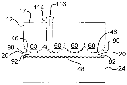
[0004] An electrophoresis medium 20 is maintained adjacent the
portions of beads 14 which protrude inwardly from material 16 by
CA 02643808 2008-09-10
WO 2007/118306 PCT/CA2007/000593
- 2 -
containment of medium 20 within a reservoir 22 defined by lower sheet
24. An inert, low refractive index (i.e. less than about 1.35), low
viscosity, electrically insulating liquid such as FluorinertTM perfluor-
inated hydrocarbon liquid (1)3-1.27) available from 3M, St. Paul, MN
is a suitable electrophoresis medium. Other liquids, or water can also
be used as electrophoresis medium 20. A bead:liquid TIR interface is
thus formed. Medium 20 contains a finely dispersed suspension of light
scattering and/or absorptive particles 26 such as pigments, dyed or
otherwise scattering/absorptive silica or latex particles, etc. Sheet 24's
optical characteristics are relatively unimportant: sheet 24 need only
form a reservoir for containment of electrophoresis medium 20 and
particles 26, and serve as a support for backplane electrode 48.
[0005] As is well known, the TIR interface between two media
having different refractive indices is characterized by a critical angle k.
Light rays incident upon the interface at angles less than 0, are transmit-
ted through the interface. Light rays incident upon the interface at
angles greater than 9, undergo TIR at the interface. A small critical
angle is preferred at the TIR interface since this affords a large range of
angles over which TIR may occur.
[0006] In the absence of electrophoretic activity, as is illustrated to
the right of dashed line 28 in Figure 1A, a substantial fraction of the
light rays passing through sheet 12 and beads 14 undergoes TIR at the
inward side of beads 14. For example, incident light rays 30, 32 are
refracted through material 16 and beads 14. The rays undergo TIR two
or more times at the bead:liquid TIR interface, as indicated at points 34,
36 in the case of ray 30; and indicated at points 38, 40 in the case of
ray 32. The totally internally reflected rays are then refracted back
through beads 14 and material 16 and emerge as rays 42, 44 respec-
tively, achieving a "white" appearance in each reflection region or
pixel.
CA 02643808 2008-09-10
WO 2007/118306
PCT/CA2007/000593
-3 -
[0007] A voltage can be applied across medium 20 via electrodes
46, 48 (shown as dashed lines) which can for example be applied by
vapour-deposition to the inwardly protruding surface portion of beads
14 and to the outward surface of sheet 24. Electrode 46 is transparent
and substantially thin to minimize its interference with light rays at the
bead:liquid TIR interface. Backplane electrode 48 need not be transpar-
ent. If electrophoresis medium 20 is activated by actuating voltage
source 50 to apply a voltage between electrodes 46, 48 as illustrated to
the left of dashed line 28, suspended particles 26 are electrophoretically
moved into the region where the evanescent wave is relatively intense
(i.e. within 0.25 micron of the inward surfaces of inwardly protruding
beads 14, or closer). When electrophoretically moved as aforesaid,
particles 26 scatter or absorb light, thus frustrating or modulating TIR
by modifying the imaginary and possibly the real component of the
effective refractive index at the bead:liquid TIR interface. This is
illustrated by light rays 52, 54 which are scattered and/or absorbed as
they strike particles 26 inside the thin (-0.5 lam) evanescent wave
region at the bead:liquid TIR interface, as indicated at 56, 58 respec-
tively, thus achieving a "dark" appearance in each TIR-frustrated non-
reflective absorption region or pixel. Particles 26 need only be moved
outside the thin evanescent wave region, by suitably actuating voltage
source 50, in order to restore the TIR capability of the bead:liquid TIR
interface and convert each "dark" non-reflective absorption region or
pixel to a "white" reflection region or pixel.
[0008] As described above, the net optical characteristics of
outward sheet 12 can be controlled by controlling the voltage applied
across medium 20 via electrodes 46, 48. The electrodes can be seg-
mented to control the electrophoretic activation of medium 20 across
separate regions or pixels of sheet 12, thus forming an image.
[0009] Figure 2 depicts, in enlarged cross-section, an inward
hemispherical or "hemi-bead" portion 60 of one of spherical beads 14.
CA 02643808 2008-09-10
WO 2007/118306 PCT/CA2007/000593
- 4 -
Hemi-bead 60 has a normalized radius r = 1 and a refractive index Th.
A light ray 62 perpendicularly incident (through material 16) on hemi-
bead 60 at a radial distance a from hemi-bead 60's centre C encounters
the inward surface of hemi-bead 60 at an angle 64/ relative to radial axis
66. For purposes of this theoretically ideal discussion, it is assumed
that material 16 has the same refractive index as hemi-bead 60 (i.e.
r1i= 2,so ray 62 passes from material 16 into hemi-bead 60 without
refraction. Ray 62 is refracted at the inward surface of hemi-bead 60
and passes into electrophoretic medium 20 as ray 64 at an angle 02
relative to radial axis 66.
[0010] Now consider incident light ray 68 which is perpendicularly
incident (through material 16) on hemi-bead 60 at a distance a = 113
111
from hemi-bead 60's centre C. Ray 68 encounters the inward surface
of hemi-bead 60 at the critical angle k (relative to radial axis 70), the
minimum required angle for TIR to occur. Ray 68 is accordingly
totally internally reflected, as ray 72, which again encounters the
inward surface of hemi-bead 60 at the critical angle oc. Ray 72 is
accordingly totally internally reflected, as ray 74, which also encounters
the inward surface of hemi-bead 60 at the critical angle O. Ray 74 is
accordingly totally internally reflected, as ray 76, which passes perpen-
dicularly through hemi-bead 60 into the embedded portion of bead 14
and into material 16. Ray 68 is thus reflected back as ray 76 in a
direction approximately opposite that of incident ray 68.
[0011] All light rays which are incident on hemi-bead 60 at dis-
tances .ct_ac. from hemi-bead 60's centre C are reflected back (but not
exactly retro-reflected) toward the light source; which means that the
reflection is enhanced when the light source is overhead and slightly
behind the viewer, and that the reflected light has a diffuse characteris-
tic giving it a white appearance, which is desirable in reflective display
applications. Figures 3A, 3B and 3C depict three of hemi-bead 60's
CA 02643808 2008-09-10
WO 2007/118306 PCT/CA2007/000593
-5 -
reflection modes. These and other modes coexist, but it is useful to
discuss each mode separately.
[0012] In Figure 3A, light rays incident within a range of distances
tie< a.al undergo TIR twice (the 2-TIR mode) and the reflected rays
diverge within a comparatively wide arc 0/ centred on a direction
opposite to the direction of the incident light rays. In Figure 3B, light
rays incident within a range of distances al < a_<a2 undergo TIR three
times (the 3-TIR mode) and the reflected rays diverge within a narrower
arc 02< 01 which is again centred on a direction opposite to the direc-
tion of the incident light rays. In Figure 3C, light rays incident within a
range of distances a2<a_a3 undergo TIR four times (the 4-TIR mode)
and the reflected rays diverge within a still narrower arc 03< 02 also
centred on a direction opposite to the direction of the incident light rays.
Hemi-bead 60 thus has a "semi-retro-reflective," partially diffuse
reflection characteristic, causing display 10 to have a diffuse appearance
akin to that of paper.
[0013] Display 10 has relatively high apparent brightness, compa-
rable to that of paper, when the dominant source of illumination is
behind the viewer, within a small angular range. This is illustrated in
Figure 1B which depicts the wide angular range a over which viewer V
is able to view display 10, and the angle p which is the angular devia-
tion of illumination source S relative to the location of viewer V.
Display's 10's high apparent brightness is maintained as long as p is not
too large. At normal incidence, the reflectance R of hemi-bead 60 (i.e.
the fraction of light rays incident on hemi-bead 60 that reflect by TIR)
is given by equation (1):
\2
R=1¨ 773 (1)
where m is the refractive index of hemi-bead 60 and rh is the refractive
index of the medium adjacent the surface of hemi-bead 60 at which TIR
CA 02643808 2008-09-10
WO 2007/118306
PCT/CA2007/000593
- 6 -
occurs. Thus, if hemi-bead 60 is formed of a lower refractive index
material such as polycarbonate (7)1-1.59) and if the adjacent medium is
Fluorinert (r73-1.27), a reflectance R of about 36% is attained, whereas if
hemi-bead 60 is formed of a high refractive index nano-composite mate-
rial (1/1-1.92) a reflectance R of about 56% is attained. When illumina-
tion source S (Figure 1B) is positioned behind viewer V's head, the
apparent brightness of display 10 is further enhanced by the aforemen-
tioned semi-retro-reflective characteristic.
[0014] As shown in Figures 4A-4G, hemi-bead 60's reflectance is
maintained over a broad range of incidence angles, thus enhancing
display 10's wide angular viewing characteristic and its apparent bright-
ness. For example, Figure 4A shows hemi-bead 60 as seen from perpen-
dicular incidence¨that is, from an incidence angle offset 0 from the
perpendicular. In this case, the portion 80 of hemi-bead 60 for which
appears as an annulus. The annulus is depicted as white, corre-
sponding to the fact that this is the region of hemi-bead 60 which reflects
incident light rays by TIR, as aforesaid. The annulus surrounds a circu-
lar region 82 which is depicted as dark, corresponding to the fact that this
is the non-reflective region of hemi-bead 60 within which incident rays
are absorbed and do not undergo TIR. Figures 4B-4G show hemi-bead
60 as seen from incident angles which are respectively offset 15 , 30 ,
45 , 60 , 75 and 90 from the perpendicular. Comparison of Figures
4B-4G with Figure 4A reveals that the observed area of reflective portion
80 of hemi-bead 60 for which a_cie decreases only gradually as the
incidence angle increases. Even at near glancing incidence angles (e.g.
Figure 4F) an observer will still see a substantial part of reflective portion
80, thus giving display 10 a wide angular viewing range over which high
apparent brightness is maintained.
[0015] Display 10 can exhibit undesirable clustering of particles 26
over time. More particularly, particles 26 tend to form loose agglomer-
ates within electrophoretic medium 20, with the surrounding regions of
CA 02643808 2008-09-10
WO 2007/118306 PCT/CA2007/000593
- 7 -
electrophoretic medium 20 containing relatively few suspended particles
26. Such clustering of absorptive particles 26 can cause long-term
deterioration of display 10's image quality and overall performance. As
explained below, it is possible to electrophoretically frustrate TIR in
display 10 without employing particles 26, thus reducing display 10's
susceptibility to shortcomings caused by particle agglomeration.
[0016] The foregoing examples of the related art and limitations
related thereto are intended to be illustrative and not exclusive. Other
limitations of the related art will become apparent to those of skill in the
art upon a reading of the specification and a study of the drawings.
Brief Description of Drawings
[0017] Exemplary embodiments are illustrated in referenced figures
of the drawings. It is intended that the embodiments and figures dis-
closed herein are to be considered illustrative rather than restrictive.
[0018] Figure lA is a greatly enlarged, not to scale, fragmented
cross-sectional side elevation view, of a portion of an electrophoretically
frustrated or modulated prior art reflective image display.
[0019] Figure 1B schematically illustrates the wide angle viewing
range a of the Figure lA display, and the angular range 0 of the illumi-
nation source.
[0020] Figure 2 is a greatly enlarged, cross-sectional side elevation
view of a hemispherical ("hemi-bead") portion of one of the spherical
beads of the Figure 1A apparatus.
[0021] Figures 3A, 3B and 3C depict semi-retro-reflection of light
rays perpendicularly incident on the Figure 2 hemi-bead at increasing off-
axis distances at which the incident rays undergo TIR two, three and four
times respectively.
[0022] Figures 4A, 4B, 4C, 4D, 4E, 4F and 4G depict the Figure 2
hemi-bead, as seen from viewing angles which are offset 0 , 15 , 30 ,
45 , 60 , 75 and 90 respectively from the perpendicular.
CA 02643808 2008-09-10
WO 2007/118306 PCT/CA2007/000593
- 8 -
[0023] Figures 5A and 5B are greatly enlarged, not to scale, frag-
mented cross-sectional side elevation views of a portion of an electro-
phoretically frustrated (i.e. modulated) reflective image display incorpo-
rating light absorbing, electrostatically charged ions.
[0024] Figure 6 is a greatly enlarged, not to scale, fragmented
cross-sectional side elevation view of a portion of an electrophoretically
frustrated (i.e. modulated) reflective image display incorporating a
nanostructured or nanoporous electrically conductive coating.
[0025] Figure 7 is a top plan (i.e. as seen from a viewing angle
offset 00 from the perpendicular) cross-sectional view of a portion of the
Figure 1A display, showing the spherical beads arranged in a hexagonal
closest packed (HCP) structure.
[0026] Figures 8A and 8B are top plan views, on a greatly enlarged
scale, of two alternative backplane electrode patterns for use with the
Figure 7 structure.
[0027] Figures 9A and 9B are greatly enlarged, not to scale, frag-
mented cross-sectional side elevation views of a portion of an electro-
phoretically frustrated (i.e. modulated) reflective image display the
Figure 8A backplane electrode pattern and incorporating light absorbing,
electrostatically charged ions.
Description
[0028] Throughout the following description specific details are set
forth in order to provide a more thorough understanding to persons
skilled in the art. However, well known elements may not have been
shown or described in detail to avoid unnecessarily obscuring the disclo-
sure. Accordingly, the description and drawings are to be regarded in an
illustrative, rather than a restrictive, sense.
[0029] As shown schematically in Figures 5A, 5B invisibly small
light absorbing, soluble molecules such as dye molecules are dissolved in
CA 02643808 2008-09-10
WO 2007/118306
PCT/CA2007/000593
- 9 -
an inert, low refractive index (i.e. less than about 1.35), low viscosity
liquid electrophoretic medium 20, such as water. When dissolved, the
molecules dissociate into electrostatically charged ions. Medium 20
accordingly contains a large number of light absorbing, electrostatically
charged ions which can be electrophoretically moved into or out of the
evanescent wave region at the aforementioned bead:liquid TIR interface
by applying an appropriate electric field.
[0030] More particularly, when dissolved, the molecules dissociate
into at least one electrostatically positively charged ion species and at
least one electrostatically negatively charged ion species, with the number
of positive charges equaling the number of negative charges such that
medium 20 overall has an electrostatically neutral charge. Typically only
one ion species is light absorbing¨the other species being a counter-ion
which balances the total charge of the dissolved molecule. Persons
skilled in the art will understand that a molecule's dissociation into its
ionic constituents does not involve a chemical reaction since the chemical
nature of the constituents does not change.
[0031] When electrophoresis medium 20 is activated by actuating
voltage source 50 to apply a first voltage between electrodes 46, 48 a
large number of light absorbing ions dissolved in medium 20 are electro-
phoretically moved into and concentrated within region 90 adjacent
electrode 46 against the inward sides of hemi-beads 60. Simultaneously,
light absorbing ions dissolved in medium 20 are electrophoretically
moved out of region 92 adjacent electrode 48. Ions which move out of
region 92 do not move into region 90, but remain within medium 20,
between regions 90, 92.
[0032] Figure 5A depicts the non-reflective state, in which region
90 is a "concentration region" containing a sufficiently large number of
light absorbing ions to substantially cover the inward surfaces of hemi-
beads 60. Persons skilled in the art will understand that the thickness of
region 90 depends on the type of ions and their concentration in medium
CA 02643808 2008-09-10
WO 2007/118306
PCT/CA2007/000593
- 10 -
20, but region 90 is typically much thinner than the evanescent wave
region. Region 90 consequently lies within the evanescent wave region,
so the light absorbing ions in region 90 absorb light rays (e.g. ray 114)
which are incident upon reflective annular region 80 by frustrating or
modulating TIR as aforesaid, and also absorb light rays (e.g. rays 116)
which do not undergo TIR and which would otherwise pass through
beads 14. The light absorbing, electrostatically charged ions need not
completely cover the inward surfaces of hemi-beads 60, since as previ-
ously explained in relation to Figure 2, many incident light rays interact
several times with each hemi-bead 60 so substantial coverage results in an
acceptable level of light absorption. In the Figure 5A non-reflective
state, region 92 is a "depletion region" containing a comparatively small
number of light absorbing, electrostatically charged ions. The depletion
region has no significant optical function in the non-reflective state, other
than serving as a source of light absorbing, electrostatically charged ions.
[0033] In the reflective state¨shown in Figure 5B¨ voltage source
50 is actuated to apply a second voltage, having opposite polarity to the
first voltage, between electrodes 46, 48. Consequently, the light absorb-
ing, electrostatically charged ions are electrophoretically moved out of
region 90, which, in the reflective state, becomes a depletion region
containing a comparatively small number of light absorbing ions. Simul-
taneously, a large number of light absorbing ions suspended in medium
20 are electrophoretically moved into and concentrated within region 92
adjacent electrode 48, which, in the reflective state, becomes a concentra-
tion region containing a sufficiently large number of light absorbing ions
to substantially cover the outward surface of electrode 48. Light absorb-
ing ions which move out of region 90 do not move into region 92, but
remain within medium 20, between regions 90, 92.
[0034] In the Figure 5B reflective state, the comparatively small
number of light absorbing ions in region 90 enables light rays (e.g. ray
114) which are incident upon one of hemi-bead 60s' reflective annular
CA 02643808 2008-09-10
WO 2007/118306
PCT/CA2007/000593
- 11 -
regions 80 to undergo TIR as aforesaid. Light rays (e.g. rays 116) which
pass through hemi-beads 60 are absorbed by the comparatively large
number of light absorbing ions in region 92.
[0035] TIR frustration can be increased in the Figure 5A non-
reflective state by increasing the absorption cross-section of the molecules
which are dissolved in medium 20. More particularly, the dissolved
molecules dissociate into electrostatically charged light absorbing ions
having an absorption cross-section Ac, in accordance with the equation:
I = ioe_nA,x
where I is the initial intensity of light passing through medium 20 along a
path of length x, n is the number density (in units of m-3) of light absorb-
ing ions in the medium, A, is expressed in units of in-2, and I is the
resultant light intensity. It is thus apparent that any increase in A, (i.e.
by
selecting molecules having a larger A, characteristic) decreases the
resultant light intensity I, for a given path length x and given ion number
density n. A molecule's absorption cross-section is related to, but not
strictly dependent on the molecule's size. Thus, a larger dye molecule
would normally, but not always, have a larger absorption cross-section
than a smaller dye molecule. As one example, polymer dye molecules
having many monomer units and a single electron charge may be dis-
solved in medium 20. Each such molecule may be up to 10 nm long, it
being noted that 10 nm is substantially smaller than the thickness (-0.5
[im) of the evanescent wave region. Since the molecules are relatively
small, they are quickly and readily diffused into the evanescent wave
region to frustrate TIR¨a useful feature for any TIR-modulated device
such as a reflective image display.
[0036] It is advantageous to prevent electrolysis or other electro-
chemical reactions from occurring at the surface of electrodes 46, 48
since such reactions may change the electrostatic charge characteristics of
the light absorbing ions and may also cause irreversible chemical changes
CA 02643808 2012-06-07
WO 2007/118306
PCT/CA2007/000593
- 12 -
to electrodes 46, 48. This can be accomplished by coating electrodes 46,
48 with a thin (i.e. <10 1..tm) layer of insulating material such as a
vapour-deposited oxide coating:, or by adapting voltage source 50 to apply
a sufficiently low voltage (i.e. <1V) such that electrochemical reaction
does not occur.
[0037} = TIR frustration can also be increased in the non-reflective
state by increasing the effective surface area of electrodes 46, 48; thereby
increasing their capacitance and consequently increasing the amount of
charge transferred between the electrodes in response to an applied
electric field. This can be achieved as shown in Figure 6 by coating
electrodes 48, 48 with thin (i.e. <250 rim) layers 94, 96 of transparent,
electrically-conductive nano-structured or nano-porous material such as a
carbon nanotube fihn as described in "Transparent Conductive Carbon
Nanombe Films," Z. Wu et al., Science Vol. 305, No. 5668, pp. 1273-
1276, or with a porous transparent conductive coating fabricated by the
glancing angle deposition (GLAD) technique described by Robbie et al in
United States Patent Nos. 5,866,204; 6,206,065; and 6,248,422,
[0038] Nano-structured or nano-porous layers 94, 96 can yield an
effective surface area several hundred times larger than that of an
equally-sized non-nano-structured or non-nano-porous layer. The surface
features of nano-structured or nano-porous layers 94, 96 are character-
ized by dimensions on the order of about 1. to 100 run, which is much
smaller than the wavelength of light ( ¨500 nm). Consequently, nano-
structured or nano-porous layers 94, 96 do not interfere with TIR of light
rays. Although nano-structured or nano-porous layers 94, 96 are trans-
versely electrically conductive (i.e. in the direction substantially perpen-
dicular to flat outward viewing surface 17) they need not have high
lateral electrical conductivity (i.e. in the direction substantially parallel
to
flat outward viewing surface 17) since electrodes 46, 48 have high lateral
CA 02643808 2008-09-10
WO 2007/118306
PCT/CA2007/000593
- 13 -
electrical conductivity. However, if nano-structured or nano-porous
layers 94, 96 have sufficient lateral electrical conductivity, electrodes 46,
48 are not required.
[0039] An estimate of the reflectance of an array of hemispheres
corresponding to the inward "hemi-bead" portions of each one of spheri-
cal beads 14 depicted in Figure 1A can be obtained by multiplying the
reflectance of an individual hemi-bead by the hemi-beads' packing
efficiency coefficient f. Calculation of the packing efficiency coefficient f
of a closely packed structure involves application of straightforward
geometry techniques which are well known to persons skilled in the art.
The hexagonal closest packed (HCP) structure depicted in Figure 7 yields
a packing efficiency focrt/(6.tan 300) - 90.7% assuming beads 14 are of
uniform size.
[0040] Although the HCP structure yields the highest packing
density for hemispheres, it is not necessary to pack the hemi-beads in a
regular arrangement, nor is it necessary that the hemi-beads be of uni-
form size. A random distribution of non-uniform size hemi-beads having
diameters within a range of about 1-50 p.m has a packing density of
approximately 80%, and has an optical appearance substantially similar to
that of an HCP arrangement of uniform size hemi-beads. For some
reflective display applications, such a randomly distributed arrangement
may be more practical to manufacture, and for this reason, somewhat
reduced reflectance due to less dense packing may be acceptable. How-
ever, for simplicity, the following description focuses on the Figure 7
HCP arrangement of uniform size hemi-beads, and assumes the use of
materials which yield a refractive index ratio niin3 =1.5. These factors
are not to be considered as limiting the scope of this disclosure.
[0041] The above-described "semi-retro-reflective" characteristic is
important in a reflective display because, under typical viewing condi-
tions where light source S is located above and behind viewer V, a
CA 02643808 2008-09-10
WO 2007/118306 PCT/CA2007/000593
- 14 -
substantial fraction of the reflected light is returned toward viewer V.
This results in an apparent reflectance which exceeds the value
( 2
R =1¨ ¨r13 by a
"semi-retro-reflective enhancement factor" of about
171)
1.5 (see "A High Reflectance, Wide Viewing Angle Reflective Display
Using Total Internal Reflection in Micro-Hemispheres," Mossman, M.A.
et al., Society for Information Display, 23rd International Display
Research Conference, pages 233-236, September 15-18, 2003, Phoenix,
AZ). For example, in a system where the refractive index ratio ml r3
=1.5, the average surface reflectance, R, of 55% determined in accor-
dance with Equation (1) is enhanced to approximately 85% under the
semi-retro-reflective viewing conditions described above.
[0042] Individual hemi-beads 60 can be invisibly small, within the
range of 2-50 inn in diameter, and as shown in Figure 7 they can be
packed into an array to create a display surface that appears highly
reflective due to the large plurality of tiny, adjacent, reflective annular
regions 80. In these regions 80, where TIR can occur, neither particles
26 (Figure 1A) nor light absorbing ions (Figures 5A, 5B) impede the
reflection of incident light when they are not in contact with the inward,
hemispherical portions of beads 14. However, in regions 82 and 84,
where TIR does not occur, particles 26 (or light absorbing ions) may
absorb incident light rays¨even if the particles (or ions) are moved
outside the evanescent wave region so that they are not in optical contact
with the inward, hemispherical portions of beads 14. The refractive
index ratio rh/n3 can be increased in order to increase the size of each
reflective annular region 80 and thus reduce such absorption losses.
Non-reflective regions 82, 84 cumulatively reduce display 10's overall
surface reflectance, R. Since display 10 is a reflective display, it is
clearly desirable to minimize such reduction.
CA 02643808 2008-09-10
WO 2007/118306
PCT/CA2007/000593
- 15 -
[0043] This can be achieved by forming backplane electrode 48 on
sheet 24 using either one of patterns 100 or 102 depicted in Figures 8A
or 8B respectively. Black regions 104, 106 are electrically conductive
regions, and may be either reflective or non-reflective. White regions
108, 110, 112 are reflective regions, and may be either electrically
conductive or non-conductive--provided there is no electrical conductiv-
ity between regions 108, 110, 112 on the one hand and regions 104, 106
on the other hand.
[0044] Reflective regions 108, 110 are each preferably circular in
shape, and have a diameter greater than or equal to (preferably equal to)
the diameter of one of the non-reflective, circular regions 82 of one of
hemi-beads 60. Pattern 100's regions 104 have an overall size and shape
substantially similar to the overall size and shape of regions 80, 84 of
hemi-beads 60.
[0045] The optical properties of regions 104, 106 are relatively
unimportant, as are those of sheet 24. It may however be advantageous
to provide a reflective outward surface on sheet 24 and to form regions
104 (or 106) thereon, with the remaining portions of sheet 24's reflective
outward surface constituting regions 108 (or 110, 112).
[0046] When used as explained below, patterned backplane elec-
trode 100 decreases absorptive losses due to light absorption in regions
82, but does not decrease absorptive losses due to light absorption in gap
regions 84. By contrast, when used as explained below, patterned back-
plane electrode 102 decreases absorptive losses due to light absorption in
both regions 82 and 84. This is achieved by forming pattern 102 with
each one of reflective regions 112 having a size and shape which is
substantially similar to the size and shape of one of gaps 84, with each
region 112 in the same location relative to its adjacent reflective regions
110 as the location of a corresponding one of gaps 84 relative to that
gap's adjacent regions 82.
CA 02643808 2008-09-10
WO 2007/118306
PCT/CA2007/000593
- 16 -
[0047] Patterned backplane electrode 100 (or 102) is positioned
with respect to monolayer 18 to align each circular reflective region 108
(or 110) with a corresponding one of non-reflective, circular regions 82;
thereby also aligning electrically conductive region 104 (or 106) with
reflective regions 80. Figures 9A and 9B depict a reflective image
display incorporating patterned backplane electrode 100 aligned as
aforesaid, and incorporating light absorbing, electrostatically charged
ions. Operation in the non-reflective state, depicted in Figure 9A, is
substantially similar to the non-reflective state operation previously
described in relation to Figure 5A, and need not be described further.
[0048] In the reflective state¨shown in Figure 9B¨when voltage
source 50 is actuated to apply an appropriate voltage between electrodes
46, 104 the light absorbing ions are electrophoretically moved out of
region 90, which, in the reflective state, becomes a depletion region
containing a comparatively small number of light absorbing ions. Simul-
taneously, large numbers of light absorbing ions suspended in medium 20
are electrophoretically moved into and concentrated within regions 92
adjacent each electrically conductive region 104 of patterned backplane
electrode 100 (or to the electrically conductive regions 106 of a patterned
backplane electrode 102 if it is substituted for patterned backplane elec-
trode 100). Since regions 104 are aligned with the reflective annular
regions 80 of hemi-beads 60, the light absorbing ions are concentrated
away from reflective regions 108 of patterned backplane electrode 100.
Relatively few light absorbing ions remain in medium 20 outside regions
92, significantly reducing light absorption in medium 20 between the non-
reflective circular regions 82 of hemi-beads 60 and the reflective regions
108 of patterned backplane electrode 100.
[0049] Light rays (e.g. ray 114 in Figure 9B) which are incident
upon one of hemi-bead 60s' reflective annular regions 80 undergo TIR as
aforesaid. Since relatively few light absorbing ions remain in medium 20
outside regions 92, most light rays (e.g. rays 116 in Figure 9B) which do
CA 02643808 2008-09-10
WO 2007/118306 PCT/CA2007/000593
- 17 -
not undergo TIR are able to pass through medium 20 to one of reflective
regions 108 and those rays are therefore also reflected.
[0050] Advantageously, the concentration of light absorbing ions in
electrophoretic medium 20 is sufficiently high to achieve good light
absorption in the Figure 9A non-reflective state, and sufficiently low that
most light absorbing ions in medium 20 are concentrated toward elec-
trode 48 in the Figure 9B reflective state to reduce the amount of light
absorbed by ions remaining in medium 20 outside regions 92 in the
reflective state.
[0051] If hemi-bead monolayer 18 is positioned an appropriate
distance above reflective regions 108, the transmitted light rays are
focused toward reflective annular regions 80, such that the light rays are
returned approximately in the direction from which they came. This
further enhances the display's semi-retro-reflective characteristic, and can
result in a perceived reflectance value exceeding 100%. Even with the
absorptive losses associated with a red-green-blue (RGB) colour filter
array, patterned backplane electrodes 100, 102 facilitate production of
reflective image displays having a brightness comparable to that of
coloured ink on white paper.
[0052] Persons skilled in the art will understand that nano-
structured
or nano-porous layers 94, 96 previously described in relation to Figure 6
can be applied to the embodiment of Figures 9A, 9B. Persons skilled in
the art will also understand that a wide range of lens concentration
structures, semi-retro-reflective reflectors and/or semi-specular reflectors
can be applied to any of the embodiments of Figures 5A, 5B; 6; or 9A,
9B.
[0053] Substitution of light absorbing, electrostatically charged
ions
for absorptive particles 26 provides advantages besides the aforemen-
tioned reduction of susceptibility to shortcomings caused by particle
CA 02643808 2012-06-07
WO 2007/118306
PCT/CA2007/000593
- 18 -
agglomeration. For example, a display incorporating light absorbing,
electrostatically charged ions can be switched more quickly between the
reflective and non-reflective states than a prior art display incorporating
absorptive particles 26, since the ions are much smaller than and thus
have greater electrophoretic mobility than particles having approximately
the same electrostatic charge. A display incorporating light absorbing,
electrostatically charged ions also has lower voltage requirements thnt a
prior art display incorporating absorptive particles 26. For example, a
display incorporating light absorbing, electrostatically charged ions can
be operated below 1 volt, which is also advantageous to prevent electrol-
ysis or other electrochemical reactions from occurring at the surface of
electrodes 46, 48. A display incorporating light absorbing, electrostati-
cally charged ions is also less likely to develop a hysteresis response
characteristic¨hysteretic response being a shortcoming of prior art
displays incorporating absorptive particles. Furthermore, a display
incorporating light absorbing, electrostatically charged ions has greater
chemical purity than a prior art display incorporating absorptive particles,
since commercially available pigment particles 26 or other suitable
particles 26 tend to have variable have chemical purity due to impurities
which can cause unpredictable and undesirable display behaviour.
[0054] While a number of exemplary aspects and embodiments
have been discussed above, those of skill in the art will recognize certain
modifications, permutations, additions and sub-combinations thereof.
For example, TIR frustration by electrophoretic movement of light
absorbing, electrostatically charged ions can be applied not only to hemi-
beaded surfaces but also to any microstructured or nanostructured surface
having the characteristic that a substantial portion of the light rays nor-
mally incident on the microstructures or nonostructures undergoes TIR.
CA 02643808 2012-06-07
=
WO 2007/118306
PCT/CA2007/000593
- 19 -
The scope of the claims should not be limited by the preferred
embodiments set forth herein, but should be given the broadest
interpretation consistent with the description as a whole.