Note: Descriptions are shown in the official language in which they were submitted.
CA 02643847 2010-07-09
1
Method for producing implant structures for contacting or
electrostimulation of living tissue cells or nerves
The present invention relates generally to implant
structures and systems that serve for contacting living
tissue or nerves. The invention relates in particular to a
method for producing multilayered implant structures
(multilayer-system implant structures, or multilayers) with
at least one conductor-track plane having electrical
conductor tracks for the electrical contacting of implants
that serve for contacting or electrostimulation of living
tissue cells or nerves.
Devices in the form of implants for stimulating living
tissue, such as, for example, implants for the retina of
the human eye or for the human inner ear, are known. As a
rule, such implants include a number of stimulating
electrodes, via which the electrical stimulating pulses are
output to the surrounding tissue or to the cells, in order
in this way to stimulate the nerves and hence to re-
establish or improve the function thereof.
Known implants are frequently an integral part of systems
that include electrical or electronic components for
sensoric or diagnostic purposes, such as, for example, the
electrical measurement of bodily functions, blood pressure,
blood sugar or temperature. Stimulating systems may
contain components for actoric purposes, such as, for
example, for electrostimulation, defibrillation, emission
CA 02643847 2008-09-03
2
of sound, or emission of ultrasound. As a rule, such
systems include a substrate in the form of a printed
circuit board, on which the electronic devices are
arranged, with electrical contacts that are in direct or
indirect contact with the body tissue, such as, for
example, nerve tissue and muscle tissue, or with body
fluids.
In order to keep the dimensions of the electrical or
electronic components as small as possible, in addition to
ceramic substrates flexible printed circuit boards made of
plastics are also being increasingly employed. Such
flexible printed circuit boards can be structured with the
aid of established processes for producing microchips in
very fine dimensions with a layer thickness of the
conductor tracks up to a few hundred nanometres and with a
thickness of the conductor track of, for example, a few
micrometres.
Such a flexible printed circuit board consists, as a rule,
of one or more insulating layers - for example, made of
polyimide, parylenes, other plastics or insulators - on
which conductor tracks, contact areas or, where
appropriate, through-metallised holes are established
between several conductor-track planes. For the electrical
contacting of the conductor tracks, corresponding contact
points are provided, via which, for example, external
electrical lines and/or external devices can be connected,
in order to connect the electronic components on the
printed circuit board to external components of the
stimulating system.
For the purpose of producing the flexible printed circuit
boards, as a rule multilayer systems or so-called
CA 02643847 2008-09-03
3
multilayers are generated which consist of several layers.
These layers of the multilayer may include a number of
conductor-track planes or conductor-track layers, in which
electrically conducting conductor tracks are provided, and
may also have a number of insulating layers which, for
example, are arranged between two conductor-track layers,
in order to insulate the latter from one another
electrically.
Such multilayers frequently contain a relatively large
number of individual structures which are simultaneously
processed and built up on a common substrate. After the
manufacturing procedure has been concluded, the multilayer
has to be released from the substrate for further
processing. Various techniques are described in the
literature for releasing the processed multilayer systems
from the substrate, wherein a release layer is applied and,
after completion of the manufacturing process, is removed
with a suitable means. The release layer may, for example,
consist of photoresist, Si02, polymers, metals etc.
However, no technique is known in which the individual
structures are preserved in the composite in the course of
release from the substrate. In the known methods for
production and release, the individual structures can only
be released in separated form. However, the further
processing of the separated structures is associated with a
greater effort and hence also with higher costs than if the
multilayers were still present in the composite also after
their production.
It is therefore an object of the present invention to
create a method for producing multilayers that enables an
easy release from the substrate of the individual
CA 02643847 2010-07-09
4
structures that have been generated. A further object of
the present invention consists in creating a method in
which the individual structures generated on a substrate
can be jointly detached from the substrate and can thereby
be preserved in the composite.
According to the present invention, the aforementioned
object is achieved by a method for producing multilayered
implant structures with at least one conductor-track plane
with electrical conductor tracks for the electrical
contacting of, for example, implants that, for example,
serve for contacting or electrostimulation of living tissue
cells or nerves, said method comprising the following
steps:
= generating a first metal layer on a substrate,
= generating a second metal layer above the first metal
layer,
= producing a multilayer comprising a number of
multilayered implant structures above the second metal
layer,
= removing the first metal layer between the substrate
and the second metal layer, and
= releasing the multilayered implant structures from the
substrate in a coherent composite.
In this way, with the method according to the invention
there is generated between the multilayer and the substrate
a release layer consisting of two metal layers which serve
as sacrificial layer in the course of releasing the fully
CA 02643847 2008-09-03
processed multilayer by means of a wet-chemical under-
etching process. As a result, a uniform and reliable
separation of the finished multilayers from the substrate
is achieved. Hence the method according to the invention
has the advantage that all the individual-implant
structures generated on the substrate are jointly released
from the substrate in a composite and not individually.
This facilitates the subsequent technology for assembly and
interconnection with regard to automation and processing.
This advantageous effect of the method according to the
invention is based on the fact that the release of the
multilayers that have been generated is effected via a
release layer made of metal, which consists of a first and
a second metal layer which are removed together by one or
more suitable etching processes when the multilayer has
been fully processed. This release procedure is favoured
by the selection of suitable metal layers, and, as a
result, an easy release of the fully processed multilayers
from the substrate is made possible. The substrate may
consist of silicon, glass or ceramic, for example.
Whereas the first metal layer (sacrificial layer) is
preferably manufactured from chromium, the material from
which the second metal layer is generated is preferably so
chosen that the material of the second metal layer brings
about, by reason of its position in the electrochemical
series of the elements in relation to the material of the
first metal layer, a potential difference in relation to
the first metal layer. As a result, an electrochemical
voltage arises between the first metal layer (sacrificial
layer) and the second metal layer, which favours the
dissolution of the sacrificial layer in the course of the
underetching process and hence the release of the implant
CA 02643847 2008-09-03
6
structures from the substrate. By way of material for the
second metal layer, use may be made of gold, silver,
palladium or another noble metal, for example.
At high process temperatures, however, diffusion processes
may occur between the first and second metal layers which
hinder a release of the finished multilayers from the
substrate by under-etching of the sacrificial layer. This
is because at high temperatures the gold from the second
metal layer can diffuse into the first metal layer, and/or
the chromium from the first metal layer can diffuse into
the second metal layer. As a result, an alloy that is no
longer to be dissolved by an etching procedure is formed at
the boundary between the first and second metal layers. It
is therefore particularly advantageous if a third metal
layer is inserted between the first and second metal
layers, which thus serves as diffusion barrier between the
first and second metal layers.
This diffusion barrier of the third metal layer arranged
between the first and second metal layers prevents a
diffusion of gold from the second metal layer into the
first metal layer. By reason of the diffusion barrier, the
multilayers can also be processed at temperatures above
250 C. The third metal layer performs its function as
diffusion barrier between the first and the second metal
layer particularly well if the third metal layer has been
produced from titanium or tungsten titanium. The insertion
of the third metal layer does not negatively influence the
process of release of the first metal layer.
The removal of a metal layer in the method according to the
invention is typically effected via an etching process.
For an etching process, use is typically made of an etchant
CA 02643847 2008-09-03
7
that is characteristic of the respective metal of the metal
layer to be etched, and to this extent selective, with the
aid of which typically only one metal layer can be
(partially) removed in each instance. In the case of the
etching of the sacrificial layer (metal layer 1), if this
layer consists of chromium in the preferred embodiment, in
particular an acidic aqueous solution of cerium ammonium
nitrate is employed, with use typically being made of
acetic acid for the purpose of acidification. The metal
layer 3, if consisting of titanium, for example, is
typically etched with strongly diluted hydrofluoric acid;
if consisting of tungsten titanium, on the other hand,
typically with hydrogen peroxide. The etching media that
are selective for a particular metal in each instance are
known to a person skilled in the art.
In a preferred embodiment, the multilayer, which comprises
several implant structures, is surrounded by a rigid frame,
for example in the form of a fixed ring, which is formed or
applied around the implant structures of the multilayer,
preferably on the outer edge of the multilayer. In this
case the individual implant structures are connected to one
another via thin webs in the course of being released from
the substrate and are clamped in the stiff ring, enabling
simple handling of the individual implant structures. This
also facilitates the subsequent technology for assembly and
interconnection in the course of further processing of the
multilayers with regard to automation and processing. In
the course of the further processing, the webs can then be
separated, in order to obtain the fully composed individual
structures.
In a preferred embodiment of the method according to the
invention, in the course of the processing of the
CA 02643847 2008-09-03
8
multilayer at least one electrically insulating material
layer is generated, on which a conductor-track layer with
at least one conductor track is arranged.
In another preferred embodiment of the present invention,
the flexible printed circuit board for an implant consists
of several layers of an insulating material with conductor
tracks arranged between them or beneath them or above them.
A further object of the present invention consists in
making available an intermediate product for producing
implant structures, said intermediate product being
distinguished by good handling qualities and simple further
processing. This object is achieved by an intermediate
product for producing implant structures that is composed
of the following layers:
= a substrate,
= a first metal layer on the substrate,
= a second metal layer above the first metal layer and
= at least one multilayer with electrical conductor
tracks for the electrical contacting of implants that
serve for contacting or electrostimulation of living
tissue cells or nerves.
Such an implant structure can be produced by the
application of the first part of the aforementioned method
according to the present invention or is obtainable in such
a manner, whereby only the following method steps are
implemented:
= generating a first metal layer on a substrate,
= generating a second metal layer above the first metal
layer and
CA 02643847 2008-09-03
9
= producing a multilayer comprising a number of
multilayered implant structures above the second metal
layer.
Since in the case of this intermediate product the implant
structures are still located on the stable substrate layer,
the implant structures are well protected against
mechanical loads. At this stage of the intermediate
product the implant structures can therefore be transported
safely for further processing at another place. The
intermediate products for producing implant structures can
be produced by the application of the aforementioned method
according to the present invention, whereby only the
following method steps are implemented:
= removing the first metal layer between the substrate
and the second metal layer and
= releasing the multilayered implant structures from the
substrate in a coherent composite.
As a result of the application of the second part of the
aforementioned method according to the present invention on
the intermediate product, the implant structures can be
released from the substrate in a coherent composite and are
consequently present in the same form as if the implant
structures had been generated in one process after the
complete method according to the invention with the first
and second method parts.
According to a preferred embodiment, in the case of the
implant structure according to the invention a third metal
layer is provided on the first metal layer between the
first metal layer and the second metal layer. In this case
the first metal layer can be removed, in particular, by a
wet-chemical underetching process, in order to act as
CA 02643847 2008-09-03
sacrificial layer and, as a result, to detach the
multilayer from the substrate.
Further particulars, preferred embodiments and advantages
of the present invention will become apparent from the
following description with reference to the appended
drawings. Shown are:
Figure 1 a schematic representation of the configuration
of an implant structure in the first step of a
preferred embodiment of the method according to
the present invention;
Figure 2 a schematic representation of the configuration
of an implant structure in the second step of a
preferred embodiment of the method according to
the present invention;
Figure 3 a schematic representation of the configuration
of an implant structure in the third step of a
preferred embodiment of the method according to
the present invention;
Figure 4 a schematic representation of the configuration
of an implant structure in the fourth step of a
preferred embodiment of the method according to
the present invention;
Figure 5 a schematic representation of the configuration
of an implant structure in the fifth step of a
preferred embodiment of the method according to
the present invention;
{
CA 02643847 2008-09-03
11
Figure 6 a schematic representation of the configuration
of an implant structure in the sixth step of a
preferred embodiment of the method according to
the present invention;
Figure 7 a schematic representation of the configuration
of an implant structure in the seventh step of
a preferred embodiment of the method according
to the present invention;
Figure 8 a schematic representation of the configuration
of an implant structure in the eighth step of a
preferred embodiment of the method according to
the present invention; and
Figure 9 a schematic representation from above of
implant structures that have been produced in {
accordance with the method according to the
invention and that have been released from the
substrate in a composite.
The method according to the invention for producing and
releasing implant structures in a composite will be
described in the following. A schematic representation of
the configuration of an implant structure in the first step
of a preferred embodiment of the method according to the
present invention is represented in Figure 1. The method
according to the invention builds upon a substrate 4 which,
for example, consists of silicon, glass or ceramic. In the
course of the first method step, firstly a first metal
layer 1, which at a later time in the method serves as
release layer or sacrificial layer, is applied on the
substrate 4. This sacrificial layer 1 is produced, for
CA 02643847 2008-09-03
12
example, from Cr or NiCr. The first metal layer 1
preferably has a thickness from 70 nm to 200 nm.
A schematic representation of the configuration of an
implant structure in the second step of the method
according to the invention is represented in Figure 2 in a
preferred embodiment. In the course of this second method
step a third metal layer 3 is applied onto the first metal
layer 1. This third metal layer 3 is produced, for
example, from titanium or tungsten titanium, and serves
later as diffusion barrier between the first metal layer 1
and the second metal layer 2. The third metal layer 3
preferably has a thickness from 50 nm to 200 nm.
A schematic representation of the configuration of an
implant structure in the third step of the method according
to the invention is represented in Figure 3 in a preferred
embodiment. In the course of this third method step a
second metal layer 2 is applied onto the third metal layer
3, so that the third metal layer 3 is situated between the
first metal layer 1 and the second metal layer 2. It has
proved particularly advantageous if the second metal layer
2 is produced from gold. The second metal layer 2
preferably has a thickness from 50 nm to 300 nm.
Generation of the metal layers 1, 2, 3 can be effected by
suitable processes for depositing thin layers, such as, for
example, by sputtering or other suitable processes.
A schematic representation of the configuration of an
implant structure in the fourth step of the method
according to the invention is represented in Figure 4 in a
preferred embodiment. In the course of this fourth method
step, implant structures such as, for example, flexible
multilayer systems or multilayers 5 with conductor-track
CA 02643847 2008-09-03
13
planes and electrodes are processed on the second metal
layer 2, the flexible layers of the multilayer 5 being
produced from polyimide, for example. This fourth method
step of the method according to the invention may also
include several sub-processes, since in the course of these
the actual implant structures 6 are generated. In this
way, a multilayer 5 with several individual implant
structures 6 is formed above the second metal layer 2. The
processing and structuring of the multilayer 5 is effected,
for example, with the aid of lithographic processes that
are already established in microtechnology.
A schematic representation of the configuration of an
implant structure in the fifth step of the method according
to the invention is represented in Figure 5 in a preferred
embodiment. In the course of this fifth method step, the
external geometry of the individual implant structures 6 is
processed. By means of suitable structuring processes,
vertical separating gaps 7 are generated between the
individual implant structures 6, as far as the second metal
layer 2. As a result, the implant structures or
multilayers 6 are substantially separated from one another
but are still connected to one another via thin webs 10
(see Fig. 9). These connecting webs 10 are preferably
formed in the plane of the multilayers 6 and are
constructed just like the multilayer 5.
A schematic representation of the configuration of an
implant structure in the sixth step of the method according
to the invention is represented in Figure 6 in a preferred
embodiment. In the course of this sixth method step, a
wet-chemical etching of the two upper metal layers 2 and 3
is effected, i.e. at the exposed places the two upper metal
layers 2 and 3 are removed, so that the vertical separating
CA 02643847 2008-09-03
14
gaps 7 between the implant structures 6 extend as far as
the first metal layer 1. The lowest metal layer or the
first metal layer 1 (sacrificial layer) still remains.
A schematic representation of the configuration of an
implant structure in the seventh step of the method
according to the invention is represented in Figure 7 in a
preferred embodiment. In the course of this seventh method
step, the sacrificial metal layer or first metal layer 1 is
completely removed by a wet-chemical underetching, as a
result of which a horizontal separating gap 8 is formed
between the substrate 4 and the implant structures 6 in the
composite. In this method step, the etching solution
penetrates from above through the separating gaps 7 and
begins to under-etch the implant structures 6 at the
exposed places in the lateral direction, as a result of
which a horizontal separating gap 8 is generated. By
reason of the horizontal separating gap 8, the implant
structures 6 have now been released from the substrate 4
completely and in a composite.
A schematic representation of the configuration of an C
implant structure in the eighth step of the method
according to the invention is represented in Figure 8 in a
preferred embodiment. In the course of this eighth and
last method step, the two metal layers 2 and 3 that have
remained on the underside of the implant structures 6 are
removed, for example by suitable etching processes, so that {
only the implant structures 6 are left behind.
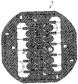
A schematic representation from above of the implant
structures 6 that have been produced by the method
according to the invention and that have been released from
the substrate in a composite is represented in Figure 9.
CA 02643847 2008-09-03
By virtue of the vertical separating gaps 7, the implant
structures 6 are substantially separated from one another
but are still connected to one another via thin webs 10.
Consequently, with the method according to the invention
the implant systems 6 can be released from the substrate 4
in a composite and processed further. This simplifies the
handling of the thin flexible multilayers 6 and facilitates
the subsequent technology for assembly and interconnection
of the implant systems 6 with regard to automation and
processing of the further treatment.
CA 02643847 2008-09-03
16
List of Reference Symbols
1 first metal layer or sacrificial layer
2 second metal layer
3 third metal layer or diffusion barrier
4 substrate
multilayer
6 implant structures
7 vertical separating gaps between the implant
structures 6
8 separating gap between the implant structures 6 and the
substrate 4
9 composite of implant structures 6
webs between the implant structures 6
}