Language selection

Search

Patent 2644078 Summary

Third-party information liability

Some of the information on this Web page has been provided by external sources. The Government of Canada is not responsible for the accuracy, reliability or currency of the information supplied by external sources. Users wishing to rely upon this information should consult directly with the source of the information. Content provided by external sources is not subject to official languages, privacy and accessibility requirements.

Claims and Abstract availability

Any discrepancies in the text and image of the Claims and Abstract are due to differing posting times. Text of the Claims and Abstract are posted:

  • At the time the application is open to public inspection;
  • At the time of issue of the patent (grant).
(12) Patent: (11) CA 2644078
(54) English Title: MODULATOR DEVICE FOR GENERATING AN OPTICAL TRANSFER SIGNAL MODULATED BY MEANS OF A BINARY SIGNAL
(54) French Title: DISPOSITIF MODULATEUR DESTINE A PRODUIRE UN SIGNAL DE TRANSFERT OPTIQUE MODULE AU MOYEN D'UN SIGNAL BINAIRE
Status: Expired and beyond the Period of Reversal
Bibliographic Data
(51) International Patent Classification (IPC):
  • H04B 10/548 (2013.01)
(72) Inventors :
  • SCHIMPE, ROBERT (Germany)
(73) Owners :
  • XIEON NETWORKS S.A.R.L.
(71) Applicants :
  • XIEON NETWORKS S.A.R.L. (Luxembourg)
(74) Agent: MARKS & CLERK
(74) Associate agent:
(45) Issued: 2013-07-09
(86) PCT Filing Date: 2007-03-02
(87) Open to Public Inspection: 2007-09-07
Examination requested: 2008-08-28
Availability of licence: N/A
Dedicated to the Public: N/A
(25) Language of filing: English

Patent Cooperation Treaty (PCT): Yes
(86) PCT Filing Number: PCT/EP2007/052005
(87) International Publication Number: EP2007052005
(85) National Entry: 2008-08-28

(30) Application Priority Data:
Application No. Country/Territory Date
10 2006 009 990.7 (Germany) 2006-03-03

Abstracts

English Abstract

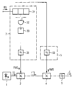
According to the invention, a very narrow-band transfer signal (LS) is generated by serially connecting a frequency modulator (2) and an amplitude modulator (4). The frequency modulator (2) is operated at a modulation index which at least largely suppresses the carrier signal (TS) while the amplitude modulator (4) suppresses the broadband portion of the spectrum by fading out the transfer signal (LS) during frequency-shift keying.


French Abstract

Selon l'invention, un signal de transmission à bande étroite (LS) est produit par une commutation en série d'un modulateur de fréquence (2) et d'un modulateur d'amplitude (4). Le modulateur de fréquence (2) fonctionne sur un indice de modulation qui supprime largement le signal de porteuse (TS) tandis que le modulateur d'amplitude (4) supprime la partie de diffusion du spectre grâce à la suppression du signal de transfert (LS) lors de la manipulation de fréquence.

Claims

Note: Claims are shown in the official language in which they were submitted.


-6-
What is claimed is:
1. A modulator for generating an optical transfer signal
modulated by a binary signal, comprising:
a frequency modulator which modulates an optical carrier
signal;
a precoder which is supplied with the binary signal and uses a
first drive circuit to control frequency shift keying by the
frequency modulator in the case of a 1-0 sequence or a 0-1 sequence
of the binary signal;
an amplitude modulator which is supplied with a frequency-
modulated signal by the frequency modulator; and
a second drive circuit for the amplitude modulator, which
circuit is supplied with the binary signal and suppresses the
frequency-modulated signal generated by the frequency modulator
during frequency shift keying and generates the optical transfer
signal with a narrow spectrum.
2. The modulator as claimed in claim 1, wherein the first drive
circuit is designed such that the frequency-modulated signal has
a modulation index of between 1.8 and 2.6.
3. The modulator as claimed in claim 1 or 2, wherein the
precoder is designed such that frequency shift keying is carried
out during a 1-0-1 sequence.
4. The modulator as claimed in any one of claims 1 to 3,
wherein at least one of the first drive circuit and the second
drive circuit is designed such that driving is effected using
sinusoidal modulation signals.
5. The modulator as claimed in any one of claims 1 to 4,
wherein the first drive circuit is designed such that frequency
shift keying is carried out within the duration of one bit.

-7-
6. The modulator as claimed in any one of claims 1 to 5,
wherein at least one of the first drive circuit and the second
drive circuit includes a controllable delay element to compensate
for the different propagation speeds of the frequency-modulated
signals.
7. The modulator as claimed in any one of claims 1 to 6,
wherein a directly modulated laser is used to generate the
carrier signal and is simultaneously used as the frequency
modulator.
8. The modulator as claimed in any one of claims 1 to 7,
wherein the first drive circuit includes a first filter
arrangement for optimum pulse shaping.
9. The modulator as claimed in any one of claims 1 to 8,
wherein the second drive circuit drives the amplitude modulator
differently on the basis of the frequency of the signal emitted
by the frequency modulator, such that the amplitude of the
transfer signal remains the same when a logic 1 is emitted.
10. The modulator as claimed in any one of claims 1 to 9,
further comprising:
a bandpass filter for eliminating signal elements with
undesirable frequencies connected downstream of the amplitude
modulator.

Description

Note: Descriptions are shown in the official language in which they were submitted.


CA 02644078 2012-08-13
- 1 -
Modulator device for generating an optical transfer signal modulated
by means of a binary signal
The invention relates to a modulator device and in particular to a
modulator for generating an optical transfer signal modulated by a
binary signal.
A laser having a downstream amplitude modulator (intensity
modulator) generates an optical spectrum with a spectral line at the
carrier frequency and a bandwidth which is wider than the bandwidth
of the information signal.
Such an emission spectrum reduces the
amount of information which can be transferred overall in a
wavelength-division multiplex system. On account of the non-linear
properties of the transmission fiber, a wider bandwidth results in
greater distortion of the transfer signal. One method for reducing
the bandwidth is duobinary coding. Such a method for reducing the
bandwidth is Technology Letters, 1998, Vol. 10, Issue 8, pp. 1159-
1161: "Prechirped Duobinary Modulation" by A. DjupsjObacka (Ericsson
Components, Sweden). However, this type of coding is very
complicated.
Therefore, the object of an aspect of the invention is to specify a
modulation device which can be implemented in a simple manner and is
intended to generate a high-quality transfer signal.
Accordingly, in one aspect there is provided a modulator for
generating an optical transfer signal modulated by a binary signal,
comprising: a frequency modulator which modulates an optical carrier
signal; a precoder which is supplied with the binary signal and uses
a first drive circuit to control frequency shift keying by the
frequency modulator in the case of a 1-0 sequence or a -1 sequence
of the binary signal; an amplitude modulator which is supplied with
a frequency-modulated signal by the frequency modulator; and a
second drive circuit for the amplitude modulator, which circuit is
supplied with the binary signal and suppresses the frequency-
modulated signal generated by the frequency modulator during
frequency shift keying and generates the optical transfer signal
with a narrow spectrum.

CA 02644078 2012-08-13
- 2 -
The advantage of an aspect of this invention is that the optical
carrier signal is frequency-modulated in such a manner that the
optical carrier is suppressed at least to a large extent. The drive
signal for the frequency modulator is pre-coded in such a manner
that frequency shift keying is respectively carried out only in the
case of a 10 or 01 change. This frequency shift keying is required
only in the case of 101 sequences. In
contrast, in the case of
longer 11 sequences or 00 sequences, no frequency shift keying is
carried out. An
amplitude modulator which suppresses the broad
signal spectrum produced during frequency shift keying is connected
downstream of the frequency modulator. As
a result, all further
spectral lines, apart from the spectral lines adjacent to the
original carrier frequency, disappear in the case of a 1010 signal
sequence. The spectrum remains narrow even in the case of a real
data signal.
The circuit can be constructed in a particularly cost-effective
manner if a directly modulated laser is used as the source of the
carrier signal and as the frequency modulator.
A suitably designed drive circuit makes it possible to compensate
for asymmetry in the amplitude, to optimize the transfer signal with
regard to a desired chirp, and to compensate for delay time
differences.
The invention is described in more detail using figures, in which:
figure 1 shows a first exemplary embodiment of the invention,
figure 2 shows a variant of the invention which can be implemented
in a cost-effective manner, and
figure 3 shows a timing diagram.
Figure 1 shows a block diagram of the modulator. A
carrier
frequency signal TS which is supplied to a frequency modulator
2 is generated by a laser 1 or another signal source.
The frequency-modulated output signal FTS from
said
frequency modulator is supplied to an amplitude modulator 5 which

CA 02644078 2008-08-28
PCT/EP2007/052005 - 3 -
2006P04412W0US
modulates on a binary signal, the data, and thus generates a
transfer signal LS. The latter is emitted via a bandpass filter
6, if necessary. The frequency modulator is controlled by the
binary signal using a first drive circuit 3 and the amplitude
modulator is controlled by the binary signal using a second
drive circuit.
The method of operation of the modulator device is now
explained in more detail using a timing diagram which is
illustrated in figure 3. The binary signal BS is illustrated in
the first row of the timing diagram. It begins with a 10101
sequence which gives rise to the broadest spectrum in the case
of modulation. It is first of all assumed that the frequency
modulator 2 carries out frequency shift keying by means of the
first drive circuit 3 for each 10 sequence. The first drive
circuit 3 contains a precoder 31, 32 having a shift register 31
and a logic circuit 32. The binary signal is written into the
shift register 31. The illustration of the binary signal BS
relates to the output of the first flip-flop of the shift
register 31 (the associated clock signal has not been
illustrated). The occurrence of a 10 sequence is checked in the
logic circuit 32. If this sequence occurs, for example after
the first logic 1 or at the beginning of the first completely
illustrated logic zero, a flip-flop 33 is triggered, with the
result that its initial state changes. A frequency modulation
signal FMS, which gives rise to frequency shift keying from the
frequency fl to f2, is generated thereby by means of a first
filter arrangement 35 which generally also carries out
electrical matching to the frequency modulator. Frequency shift
keying between f2 and fl is carried out again in the case of
the next 10 combination, which is then repeated in the case of
further 10 sequences. The frequency profile of the frequency-
modulated signal FTS corresponds to the profile of the
amplitude A of the frequency modulation signal. The modulation
index is intended to be between 1.8 and 2.6; the carrier is
suppressed in an optimum manner at approximately 2.4. An

,
CA 02644078 2008-08-28
PCT/EP2007/052005 - 3a -
2006P04412WOUS
optimum signal quality is achieved, in particular, with a
modulation index of approximately 2Ø

CA 02644078 2008-08-28
PCT/EP2007/052005 - 4 -
2006P04412WOUS
The third row shows a sinusoidal frequency modulation signal
FMS which is at half the fundamental frequency of the binary
signal in the case of a 10 sequence. It is shaped (if
necessary) by the first filter arrangement 35 which also
provides the required drive voltage for the frequency modulator
in this case.
The fourth row illustrates a frequency modulation voltage FMS1
for an advantageous variant of the modulation device, in which
unnecessary frequency shift keying is avoided. Frequency shift
keying is only carried out whenever there is a 101 sequence.
For this purpose, a further input signal is supplied to the
logic circuit via the dashed connection in figure 1.
In the fifth row, frequency shift keying is no longer carried
out by means of a sinusoidal frequency modulation voltage but
rather takes place in the half period before it. For the rest,
the FM modulation voltage FMS2 corresponds to the modulation
voltage in the third row.
The binary signal is impressed in the amplitude modulator 4. It
must always take place for the correct temporal assignment of
an amplitude modulation signal AMS to the frequency modulation
signal or at the times during which frequency shift keying is
carried out. The second row shows a square-wave (dashed)
modulation signal, which, apart from a necessary time delay,
corresponds to the binary signal BS, and the sinusoidal
amplitude modulation signal AMS. During frequency shift keying,
the frequency-modulated signal FTS must be suppressed as far as
possible and the amplitude of the transfer signal LS must thus
be zero as far as possible so that the interfering frequency
components are masked. This is the case with a combination of
the frequency modulation signal FMS and the amplitude
modulation signal AMS. The time function in the lowest, sixth
row shows the amplitude profile of the transfer signal for

CA 02644078 2008-08-28
PCT/EP2007/052005 - 5 -
2006P04412WOUS
this combination of sinusoidal amplitude modulation and
frequency modulation FMS.
If, in contrast, the variant is implemented with frequency
shift keying for 101 sequences according to row 4 or 5, the
amplitude modulation voltage must be delayed by the duration of
one bit, as illustrated in figure 2. It goes without saying
that the delay times of lines and components must be taken into
account for the high data rates.
Figure 2 shows a variant of the modulator device, in which,
instead of an external frequency modulator, a directly
frequency-modulated laser 1, 2 is used as the generator of the
carrier signal TS and as the frequency modulator. However,
amplitude modulation also always occurs in this case and should
be compensated for. In order to compensate for asymmetry in the
different amplitudes during frequency shift keying and also to
compensate for the delay times caused by dispersion of the
transmission fiber, the first drive circuit contains an
asymmetrical or controllable first delay element 34 and the
second drive circuit 5 contains an asymmetrical or controllable
second delay element 51 and a controllable attenuation element
52. The delay elements make it possible to compensate for the
different delay times of a transmission path for both shift
keying frequencies fl and f2 (this may also be carried out at
the receiving end); the controllable attenuation element 52
compensates for the different amplitudes of the frequency-
modulated signal FTS. These functions which are illustrated
only basically here can be implemented using numerous circuit
variants.

Representative Drawing
A single figure which represents the drawing illustrating the invention.
Administrative Status

2024-08-01:As part of the Next Generation Patents (NGP) transition, the Canadian Patents Database (CPD) now contains a more detailed Event History, which replicates the Event Log of our new back-office solution.

Please note that "Inactive:" events refers to events no longer in use in our new back-office solution.

For a clearer understanding of the status of the application/patent presented on this page, the site Disclaimer , as well as the definitions for Patent , Event History , Maintenance Fee  and Payment History  should be consulted.

Event History

Description Date
Time Limit for Reversal Expired 2016-03-02
Letter Sent 2015-03-02
Letter Sent 2015-01-30
Letter Sent 2014-02-03
Letter Sent 2014-01-30
Inactive: Multiple transfers 2013-12-30
Grant by Issuance 2013-07-09
Inactive: Cover page published 2013-07-08
Inactive: First IPC assigned 2013-04-29
Inactive: IPC assigned 2013-04-29
Pre-grant 2013-03-07
Inactive: Final fee received 2013-03-07
Inactive: IPC expired 2013-01-01
Inactive: IPC removed 2012-12-31
Letter Sent 2012-10-03
Notice of Allowance is Issued 2012-10-03
Inactive: Approved for allowance (AFA) 2012-09-14
Amendment Received - Voluntary Amendment 2012-08-13
Inactive: S.30(2) Rules - Examiner requisition 2012-02-14
Inactive: Cover page published 2008-12-29
Inactive: Acknowledgment of national entry - RFE 2008-12-22
Letter Sent 2008-12-22
Inactive: First IPC assigned 2008-12-16
Application Received - PCT 2008-12-15
National Entry Requirements Determined Compliant 2008-08-28
Request for Examination Requirements Determined Compliant 2008-08-28
All Requirements for Examination Determined Compliant 2008-08-28
Application Published (Open to Public Inspection) 2007-09-07

Abandonment History

There is no abandonment history.

Maintenance Fee

The last payment was received on 2013-03-04

Note : If the full payment has not been received on or before the date indicated, a further fee may be required which may be one of the following

  • the reinstatement fee;
  • the late payment fee; or
  • additional fee to reverse deemed expiry.

Patent fees are adjusted on the 1st of January every year. The amounts above are the current amounts if received by December 31 of the current year.
Please refer to the CIPO Patent Fees web page to see all current fee amounts.

Owners on Record

Note: Records showing the ownership history in alphabetical order.

Current Owners on Record
XIEON NETWORKS S.A.R.L.
Past Owners on Record
ROBERT SCHIMPE
Past Owners that do not appear in the "Owners on Record" listing will appear in other documentation within the application.
Documents

To view selected files, please enter reCAPTCHA code :


To view images, click a link in the Document Description column. To download the documents, select one or more checkboxes in the first column and then click the "Download Selected in PDF format (Zip Archive)" or the "Download Selected as Single PDF" button.

List of published and non-published patent-specific documents on the CPD .

If you have any difficulty accessing content, you can call the Client Service Centre at 1-866-997-1936 or send them an e-mail at CIPO Client Service Centre.


Document
Description 
Date
(yyyy-mm-dd) 
Number of pages   Size of Image (KB) 
Description 2008-08-27 6 244
Claims 2008-08-27 3 84
Representative drawing 2008-08-27 1 6
Drawings 2008-08-27 3 39
Abstract 2008-08-27 2 78
Description 2012-08-12 6 248
Claims 2012-08-12 2 64
Representative drawing 2013-06-16 1 4
Acknowledgement of Request for Examination 2008-12-21 1 177
Notice of National Entry 2008-12-21 1 203
Courtesy - Certificate of registration (related document(s)) 2008-12-21 1 104
Commissioner's Notice - Application Found Allowable 2012-10-02 1 162
Maintenance Fee Notice 2015-04-12 1 170
PCT 2008-08-27 3 109
Fees 2011-03-01 1 69
Correspondence 2013-03-06 2 54