Note: Descriptions are shown in the official language in which they were submitted.
CA 02644629 2008-08-28
WO 2008/054845 PCT/US2007/064720
PHOTOVOLTAIC DEVICE CONTAINING NANOPARTICLE
SENSITIZED CARBON NANOTUBES
[0001] This application claims the benefit of U.S. Provisional Patent
Application Serial No. 60/785,651, filed on March 23, 2006, under 35 U.S.C.
119(e),
which is incorporated herein by reference in its entirety.
FIELD OF THE INVENTION
[0002] The invention relates to the use of carbon nanotubes and photoactive
nanoparticles, including nanoparticles of different size and composition, to
form
photovoltaic devices.
BACKGROUND OF THE INVENTION
[0003] Increasing oil prices have heightened the importance of developing cost
effective renewable energy. Significant efforts are underway around the world
to
develop cost effective solar cells to harvest solar energy. Current solar
energy
technologies can be broadly categorized as crystalline silicon and thin film
technologies. More than 90% of the solar cells are made from silicon - single
crystal
silicon, polycrystalline silicon or amorphous silicon.
[0004] Historically, crystalline silicon (c-Si) has been used as the
light-absorbing semiconductor in most solar cells, even though it is a
relatively poor
absorber of light and requires a considerable thickness (several hundred
microns) of
material. Nevertheless, it has proved convenient because it yields stable
solar cells with
good efficiencies (12-20%, half to two-thirds of the theoretical maximum) and
uses
process technology developed from the knowledge base of the microelectronics
industry.
[0005] Two types of crystalline silicon are used in the industry. The first is
monocrystalline, produced by slicing wafers (approximately 150mm diameter and
350
microns thick) from a high-purity single crystal boule. The second is
multicrystalline
silicon, made by sawing a cast block of silicon first into bars and then
wafers. The main
1
CA 02644629 2008-08-28
WO 2008/054845 PCT/US2007/064720
trend in crystalline silicon cell manufacture is toward multicrystalline
technology. For
both mono- and multicrystalline Si, a semiconductor p-n junction is formed by
diffusing phosphorus (an n-type dopant) into the top surface of the boron
doped
(p-type) Si wafer. Screen-printed contacts are applied to the front and rear
of the cell,
with the front contact pattern specially designed to allow maximum light
exposure of
the Si material with minimum electrical (resistive) losses in the cell.
[0006] Silicon solar cells are very expensive. Manufacturing is mature and not
amenable for significant cost reduction. Silicon is not an ideal material for
use in solar
cells as it primarily absorbs in the visible region of the solar spectrum
thereby limiting
the conversion efficiency.
[0007] Second generation solar cell technology is based on thin films. Two
main thin film technologies are amorphous silicon and CIGS.
[0008] Amorphous silicon (a-Si) was viewed as the "only" thin film PV
material in the 1980s. But by the end of that decade, and in the early 1990s,
it was
dismissed by many observers for its low efficiencies and instability. However,
amorphous silicon technology has made good progress toward developing a very
sophisticated solution to these problems: multijunction configurations. Now,
commercial, multijunction a-Si modules could be in the 7%-9% efficiency range.
United Solar Systems Corporation and Kanarka plan have built 25-MW
manufacturing
facilities and several companies have announced plans to build manufacturing
plants in
Japan and Germany. BP Solar and United Solar Systems Corporation plan to build
10
MW facilities in the near future.
[0009] The key obstacles to a-Si technology are low efficiencies (about 11%
stable), light-induced efficiency degradation (which requires more complicated
cell
designs such as multiple junctions), and process costs (fabrication methods
are
vacuum-based and fairly slow). All of these issues are important to the
potential of
manufacturing cost-effective a-Si modules.
[0010] Thin film solar cells made from Copper Indium Gallium Diselenide
(CIGS) absorbers show promise in achieving high conversion efficiencies of 10-
12%.
The record high efficiency of CIGS solar cells (19.2% NREL) is by far the
highest
2
CA 02644629 2008-08-28
WO 2008/054845 PCT/US2007/064720
compared with those achieved by other thin film technologies such as Cadmium
Telluride (CdTe) or amorphous Silicon (a-Si).
[00111 These record breaking small area devices have been fabricated using
vacuum evaporation techniques which are capital intensive and quite costly. It
is very
challenging to fabricate CIGS films of uniform composition on large area
substrates.
This limitation also affects the process yield, which are generally quite low.
Because of
these limitations, implementation of evaporation techniques has not been
successful for
large-scale, low-cost commercial production of thin film solar cells and
modules and is
non-competitive with today's crystalline silicon solar modules.
[00121 To overcome the limitations of the physical vapor deposition techniques
that use expensive vacuum equipment, several companies have been developing
high
throughput vacuum processes (ex: DayStar, Global Solar) and non-vacuum
processes
(ex: ISET, Nanosolar) for the fabrication of CIGS solar cells. Using ink
technology,
very high active materials utilization can be achieved with relatively low
capital
equipment costs. The combined effect is a low-cost manufacturing process for
thin
film solar devices. CIGS can be made on flexible substrates making it possible
to
reduce the weight of solar cells. Cost of CIGS solar cells is expected to be
lower than
crystalline silicon making them competitive even at lower efficiencies. Two
main
problems with CIGS solar cells are: (1) there is no clear pathway to higher
efficiency
and (2) high processing temperatures make it difficult to use high speed roll
to roll
process and hence they will not be able to achieve significantly lower cost
structure.
[00131 These are significant problems with the currently available
technologies. Crystalline silicon solar cells which have >90% market share
today are
very expensive. Solar energy with c-silicon solar cells costs about 25 cents
per kwh as
compared to less than 10 cents per kwh for fossil fuels. In addition, the
capital cost of
installing solar panels is extremely high limiting its adoption rate.
Crystalline solar cell
technology is mature and unlikely to improve performance or cost
competitiveness in
near future. Amorphous silicon thin film technology is amenable to high volume
manufacturing that could lead to low cost solar cells. In addition, amorphous
and
microcrystal silicon solar cells absorb only in the visible region.
[0014] Next generation solar cells are required to truly achieve high
efficiencies
with light weight and low cost. Two potential candidates are (1) polymer solar
cells
3
CA 02644629 2008-08-28
WO 2008/054845 PCT/US2007/064720
and (2) nanoparticle solar cells. Polymer solar cells have the potential to be
low cost
due to roll to roll processing at moderate temperatures (< 150C). However,
polymers
suffer from two main drawbacks: (1) poor efficiencies due to slow charge
transport and
(2) poor stability- especially to UV radiation. Hence it is unlikely that
polymer solar
cells will be able to achieve the required performance to become the next
generation
solar cell. The most promising technology for the next generation solar cell
is based on
quantum dot nanoparticles.
100151 Several research groups have been conducting experimental studies on
quantum dot based solar cells. Most commonly used quantum dots are made of
compound semiconductors such as Group II-VI, II-IV and III-V. Some examples of
these photosensitive quantum dots are CdSe, CdTe, PbSe, PbS, ZnSe.
[0016] Solar cells made from photosensitive nanoparticles as described in the
art show very low efficiencies (<5%). Nanoparticies are very efficient in
generating
electron hole charge pairs when exposed to sunlight. The primary reason for
these low
efficiencies is charge recombination. To achieve high efficiencies in a solar
cell the
charges must be separated as soon as possible after they are generated.
Charges that
recombine do not produce any photocurrent and hence do not contribute towards
solar
cell efficiency. Charge recombination in nanoparticles is primarily due to two
factors:
(1) surface states on nanoparticle that facilitate charge recombination, and
(2) slow
charge transport. In the later case, charge recombination is generally faster
compared
to the charge transport rate because charges travel slowly through the
electron transport
and hole transport layers.
[0017] Various methods have been reported in the prior art to solve these
problems of nanoparticles. Surface treatment techniques have been tried to
remove
surface states. (See Furis et al, MRS Proceedings, volume 784, 2004) Such
techniques
show improvement in photoluminescence but do not improve solar conversion
efficiency as they do not impact the charge transport properties of hole
transport and
electron transport layers.
100181 It is known in the art that Ti02 layers can be used to rapidly
transport
electrons. Dye-sensitized solar cells use Ti02 precisely for this reason.
Transparent
Ti02 nanotubes have been reported in the literature (Mor et al., Adv. Funct.
Mater.,
4
CA 02644629 2008-08-28
WO 2008/054845 PCT/US2007/064720
2005, 15, 1291-1296 (2005)). These Ti02 nanotubes have been used to prepare
dye-sensitized solar cells.
100191 Single wall carbon nanotubes (SWCNT) have been used as light
absorbing material in solar cells. In addition, nanoparticles such as CdSe and
CuInS
have been covalently attached to carbon nanotubes. See Landi et al., Mater.
Res. Symp.
Proc. Vol. 836, 2005, Session L2.8 pages 1-6.
SUMMARY OF THE INVENTION
[0020] The photvoltaic devises include first and second electrodes at least
one
of which is transparent to solar radiation. A photoactive layer between the
first and
second electrodes contains photoactive nanostructures comprising carbon
nanotubes
(CNT) and photosensitive nanoparticles. The nanoparticles are closely
associated with
the carbon nanotubes and in some embodiments are covalently attached to the
CNT.
The photoactive layer is in electron conducting communication with the first
electrode
and in hole conducting communication with the second electrode. In some
embodiments the photoactive layer further comprises a conducting polymer.
[0021] In other embodiments, the photovoltaic device further includes a hole
conducting layer between the first electrode and the photoactive layer that
facilitates
hole transfer to the first electrode. In a preferred embodiment, the hole
conducting
layer contains p-type CNTs.
[0022] In the same or other embodiments, an electron conducting layer is
positioned between the second electrode and the photoactive layer to
facilitate electron
transfer to the second electrode. In a preferred embodiment, the electron
conducting
layer contains n-type CNTs.
[0023] The carbon nanotube is preferably a single wall carbon nanotube
(SWCNT). The SWCNT is preferably functionalized so as to be chemically
reactive
with the photosensitive nanoparticles of photosensitive nanoparticles that
have been
modified to contain functional groups that are reactive with the CNT/SWCNT or
a
moiety used to link the CNT/SWCNT photosensitive nanoparticle.
CA 02644629 2008-08-28
WO 2008/054845 PCT/US2007/064720
[0024] The photosensitive nanoparticles can be quantum dots, nanorods,
nanobipods, nanotripods, nanomultipods or nanowires. Preferred photosensitive
nanoparticles include CdSe, ZnSe, PbSe, InP, PbS, ZnS, Si, Ge, SiGe, CdTe,
CdHgTe,
or Group II-VI, II-IV or III-V materials. In some embodiments first and second
nanoparticle that adsorb radiation from different portions of the solar
spectrum are used
in the photovoltaic device. The first and second nanoparticles can differ in
composition, size or a combination of size and composition and absorb in
different
portions of the solar spectrum. The first and second can be nanoparticles
contained or
the same or different CNTs. For example two different photosensitive
nanoparticles
can each be associated with a single CNT. Alternatively, a first nanoparticle
can be
associated with a first CNT and a second nanoparticle with a second CNT. In
either
case a single photoactive layer can be made for such photoactive
nanostructures.
[0025] The components used in the photovoltaic device are chosen so that
appropriate band alignment exists between the photoactive nanostructure and
the
electrodes. When a conducting polymer is used in the photoactive layer, the
HOMO
and LUMO levels the conducting polymer are such that charge transfer is
facilitated
from the nanostructure to the conducting polymer and from conducting polymer
to the
electrode. Similarly, appropriate band alignment should exist between the
photoactive
layer and any electron or hole conducting layer used in the devices to
facilitate charge
extraction and charge transfer.
100261 In another embodiment, a second photoactive layer is used that contains
second photoactive nanostructures made of carbon nanotubes and nanoparticles
that
absorb radiation from different portions of the solar spectrum as compared to
the
nanoparticles of the first photoactive layer. The nanoparticles in the first
and said
second photoactive layer can differ in composition, size or a combination of
size and
composition.
100271 In some embodiments, the hole conducting layer is a hole conducting
polymer such as a p-type semiconducting polymer. Examples of p-type
semiconducting polymers include P3HT, P3OT, MEH-PPV or PEDOT. In most
embodiments, PVK is not used as a hole conducting polymer. In other
embodiments,
the hole conducting layer is a p-type semiconductor. Examples of p-type
semiconductor include p-doped Si, p-doped Ge or p-doped SiGe. In the case of
Si the
p-type semiconductor can be p-doped amorphous silicon, p-doped
microcrystalline
6
CA 02644629 2008-08-28
WO 2008/054845 PCT/US2007/064720
silicon or p-doped nanocrystalline silicon. In some cases the hole conducting
layer is
made of two or more layers of p-type semiconductor. The p-type semiconductor
layers
can be a p-doped silicon layer, a p-doped germanium layer and/or a p-doped
SiGe layer.
[0028] In a preferred embodiment the hole conducting layer contains CNTs,
preferably SWCNTs. For example, SWCNTs can be combined with p-type P3HT and
used as a hole conducting layer.
100291 In some embodiments, the electron conducting layer is an electron
conducting material such as aluminum quinolate (A1Q3) and/or n-type SWCNTs
made
by doping SWCNTs with Clz, Br2 or Cs.
BRIEF DESCRIPTION OF THE DRAWING
[0030] Figure 1(Prior Art) depicts nanometer quantum dots of different size
that absorb and emit radiation having different colors. Small dots absorb in
the blue
end of the spectrum while the large size dots absorb in the red end of the
spectrum.
[0031] Figure 2 (Prior Art) depicts quantum dots made from ZnSe, CdSe and
PbSe that absorb/emit in UV visible and IR respectively.
[0032] Figure 3 (Prior Art) depicts nanoparticles capped with solvents such as
tri-n-octyl phosphine oxide (TOPO).
[0033] Figure 4 depicts nanoparticles functionalized with an R group. The R
group can be represented as Xa-Rn-Ye where X and Y are reactive moieties such
as a
carboxylic acid (-COOH) group, a phosphoric acid (-H-'P04) group, a sulfonic
acid
(-HSO3) group or an amine, a and b are 0 or 1 where one of a and b are 1, R is
carbon,
sulfur, nitrogen and/or oxygen and n = 0-10 or 0-5.
[0034] Figure 5 depicts Functionalized Carbon Nanotube 510 containing
functional group R can be -COOH, -NH2, -P04, -HSO3, Aminoethanethiol, etc.
7
CA 02644629 2008-08-28
WO 2008/054845 PCT/US2007/064720
[0035] Figure 6 depicts a simple solar cell schematic where photosensitive
nanostructures containing photosensitive nanoparticle sensitized carbon
nanotubes
(CNTs) are sandwiched between a transparent and a metal electrode.
[0036] Figure 7 depicts a simple solar cell schematic where photoactive
nanostructures containing photosensitive nanoparticle sensitized single wall
carbon
nanotubes (SWCNT) are dispersed in a conducting polymer layer sandwiched
between
a transparent and a metal electrode.
100371 Figure 8 depicts a photosensitive nanoparticle sensitized SWCNT solar
cell design with one SWCNT interface layer 840.
[0038] Figure 9 depicts a photosensitive nanoparticle sensitized SWCNT solar
cell design with two SWCNT interface layers 930 and 950.
[0039] Figure 10 depicts photoactive nanostructures containing photosensitive
nanoparticle sensitized SWCNTs dispersed in a polymer matrix 1040 solar cell
design
with two SWCNT interface layers 1030 and 1050.
[0040] Figure 11 depicts an alternative solar cell design where a
photosensitive
nanoparticle layer 1140 is sandwiched between two SWCNT interface layers 1130
and
1150. This layer may also include photoactive nanostructures made from CNTs
and
photosensitive nanoparticles.
[0041] Figure 12 depicts another alternative solar cell design where
photosensitive layer 1240 containing photosensitive nanoparticles dispersed in
a
polymer matrix is sandwiched between two SWCNT interface layers 1230 and 1250.
This layer may also include photoactive nanostructures made from CNTs and
photosensitive nanoparticles.
100421 Figure 13 depicts a photoactive device containing two photoactive
layers. Layer 1330 contains photoactive nanostructures of CdSe-SWCNT while
layer 1340 contains CdTe-SWCNT photoactive nanostructures.
[0043] Figure 14 is similar to Figure 13 except that the photoactive
nanostructures of Layers 1430 and 1440 are dispersed in a polymer.
8
CA 02644629 2008-08-28
WO 2008/054845 PCT/US2007/064720
100441 Figure 15 depicts a solar cell design with a layer containing multiple
types of photosensitive nanoparticles 1560, 1570 and 1580 attached to SWCNTs
1530.
[0045] Figure 16 depicts a solar cell design with a layer containing multiple
SWCNTs 1630 with each SWCNT attached to one type of photosensitive
nanoparticle 1660, 1670 or 1680.
[0046] Figure 17 depicts a SWCNT 1660, 1670 or 1680 solar cell design with
multiple photoactive layers each containing photoactive nanostructures
containing
SWCNTs attached to a different type of photosensitive nanoparticle.
[0047] Figure 18 depicts a solar cell design with a photoactive layer
containing
multiple types of photosensitive nanoparticles attached to each SWCNT
sandwiched
between two SWCNT layers.
DETAILED DESCRIPTION OF THE INVENTION
[0048] An embodiment of the photovoltaic device disclosed herein is made
from two electrodes and a photoactive layer comprising photoactive
nanostructures.
The photoactive nanostructures contain at least two components: (1) CNTs
and/or
SWCNTs and (2) photosensitive nanoparticles. The nanoparticles associate with
the
surface of the CNT by self assembly and cover at least 10% of the CNT's
exterior
surface although lighter particle densities, such as 50%, 70% or 90%, can be
used. In
preferred embodiments, the nanoparticles form a monolayer covering most of the
CNT
surface.
100491 In a preferred embodiment, the nanoparticle is covalently attached to
the
CNT. This can be achieved by modifying the CNT and/or nanoparticles to contain
a
moiety/moieties that provide reactive sites for covalent linkage. In some
instances
(discussed below) a linker molecule is used to covalently attach the
nanoparticle to the
CNT.
100501 As used herein, the term "nanoparticle" or '`photosensitive
nanoparticle" refers to photosensitive materials that generate electron hole
pairs when
9
CA 02644629 2008-08-28
WO 2008/054845 PCT/US2007/064720
exposed to solar radiation. Photosensitive nanoparticles are generally
nanocrystals such
as quantum dots, nanorods, nanobipods, nanotripods, nanomultipods, or
nanowires.
100511 Photosensitive nanoparticles can be made from compound
semiconductors which include Group II-VI, II-IV and Ill-V materials. Some
examples
of photosensitive nanoparticles are CdSe, ZnSe, PbSe, InP, PbS, ZnS, CdTe Si,
Ge,
SiGe, CdTe, CdHgTe, and Group II-VI, II-IV and Ill-V materials. Photosensitive
nanoparticles can be core type or core-shell type. In a core shell
nanoparticle, the core
and shell are made from different materials. Both core and shell can be made
from
compound semiconductors.
[00521 Quantum dots are a preferred nanoparticle. As in known in the art,
quantum dots having the same composition but having different diameters absorb
and
emit radiation at different wave lengths. Figure 1 depicts three quantum dots
made of
the same composition but having different diameters. The small quantum dot
absorbs
and emits in the blue portion of the spectrum; whereas, the medium and large
quantum
dots absorb and emit in the green and red portions of the visible spectrum,
respectively.
Alternatively, as shown in Figure 2, the quantum dots can be essentially the
same size
but made from different materials. For example, a UV-absorbing quantum dot can
be
made from zinc selenide; whereas, visible and IR quantum dots can be made from
cadmium selenide and lead selenide, respectively. Nanoparticles having
different size
and/or composition can be used either randomly or in layers to produce a
broadband
solar cell that absorbs in (1) the UV and visible, (2) the visible and IR, or
(3) the UV,
visible, and IR.
[00531 The photoactive nanoparticle can be modified to contain a linker Xa-Rõ-
Yb where X and Y can be reactive moieties such as carboxylic acid groups,
phosphonic acid groups, sulfonic acid groups, amine containing groups etc., a
and b are
independently 0 or 1 where at least one of a and b is 1, R is a carbon,
nitrogen, sulfur
and/or oxygen containing group such as -CH2, -NH-, -S- and/or -0-, and n is 0-
10. One
reactive moiety can react with the nanoparticle while the other can react with
the CNT.
The linkers also passivate the nanoparticles and increase their stability,
light absorption
and photoluminescence. They can also improve the nanoparticle solubility or
suspension in common organic solvents.
CA 02644629 2008-08-28
WO 2008/054845 PCT/US2007/064720
100541 Functionalized nanoparticles are reacted with suitable reactive groups
such as hydroxyl or others on the CNTs to deposit a monolayer of dense
continuous
nanoparticles by a molecular self assembly process. By adjusting the
components of
Xa-Rn-Yb, the distance between the surface of the CNT and nanoparticle can be
adjusted to minimize the effect of surface states in facilitating charge
recombination.
The distance between these surfaces is typically 10 Angstroms or less
preferably 5
Angstroms or less. This distance is maintained so that electrons tunnel
through this gap
from the nanoparticles to the highly conducting CNTs. This facile electron
transport
helps in reducing charge recombination and results in efficient charge
separation which
leads to efficient solar energy conversion.
[0055] As used herein a "hole conducting layer" is a layer that preferentially
conducts holes. Hole transporting layers can be made from (1) inorganic
molecules
including p-doped semiconducting materials such as p-type amorphous or
microcrystalline silicon or germanium; (2) organic molecules such as
metal-thalocyanines, aryl amines etc.; (3) conducting polymers such as
polyethylenethioxythiophene (PEDOT), P3HT, P30T and MEH-PPV; and (4) p-type
CNTs or p-type SWCNTs.
[0056] As used herein an "electron conducting layer" is a layer that
preferentially conducts electrons. Electron transporting layers can be made
from
aluminum quinolate (A1Q3) and/or n-type CNTs or n-type SWCNTs.
[0057] In some embodiments, the solar cell is a broadband solar cell that is
capable of absorbing solar radiation at different wave lengths. Photosensitive
nanoparticles generate electron-hole pairs when exposed to light of a specific
wave
length. The band gap of the photosensitive nanoparticles can be adjusted by
varying the
particle size or the composition of the nanoparticles. By combining a range of
nanoparticle sizes and a range of the nanomaterials used to make the
nanoparticles,
broadband absorption over portions of or the entire solar spectrum can be
achieved.
Thus, in one embodiment, a mixture of photosensitive nanoparticles having a
different
size and/or composition can be layered on to the same or different CNTS to
make
broadband solar devices such as that set forth in Figures 13-18.
11
CA 02644629 2008-08-28
WO 2008/054845 PCT/US2007/064720
Example 1
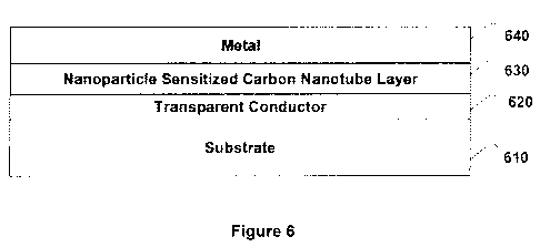
[0058] Figure 6 is a schematic of an embodiment of photosensitive nanoparticle
sensitized carbon nanotube solar cell device made secondary to the invention.
This
solar cell can be built by depositing photoactive layer 630 containing
photoactive
nanostructures comprising photosensitive nanoparticle sensitized carbon
nanotubes on
a glass substrate layer 610 coated with transparent conductor layer 620 such
as ITO
followed by the deposition of cathode metal layer 640. The device (610 through
640)
or subcomponents of the device (eg. 610, 620 and 630) are annealed at 200-400
C for
6-12 hours.
[0059] Photosensitive nanoparticles can be made from Group IV, II-IV, lI-VI,
Ill-V materials. Examples of photosensitive nanoparticles include Si, Ge,
CdSe, PbSe,
ZnSe, CdTe, CdS, PbS. Nanoparticle sizes can be varied (for example: 2-lOnm)
to
obtain a range of bandgaps. These nanoparticles can be prepared by following
the
methods well known in the art. Nanoparticles can also be functionalized by
following
the methods well known in the art. Functional groups can include carboxylic (-
COOH),
amine (-NH2), Phosphonate (-P04), Sulfonate (-HSO3), Aminoethanethiol, etc.
Carbon
nanotubes can be prepared by following methods well known in the art. See,
e.g.,
Landi et al., supra. They can also be purchased from Cheap Tubes Battleboro,
VT or
Aldrich. Carbon nanotubes are preferably single wall carbon nanotubes
100601 Carbon nanotubes can be functionalized by following the methods well
known in the art. See, e.g., Landi el al., supra. And Cho et al., Advanced
Materials, 19,
232-236 (2007). Functionalized carbon nanotubes are soluble in common organic
solvents such as chloroform. Functionalized carbon nanotubes can be reacted
with
functionalized photosensitive nanoparticles with appropriate functional groups
dissolved in suitable solvent to prepare photosensitive nanoparticle
sensitized carbon
nanotubes. The density of the nanoparticle layer can be adjusted by varying
the
reaction conditions and by varying functional groups. Ideally a carbon
nanotube
densely decorated with photosensitive nanoparticles is desired. A layer of
photosensitive nanoparticle sensitized carbon nanotubes can be deposited on
ITO
coated glass substrate by spin coating or other well known molecular self
assembly
techniques. This layer can be one monolayer or multiple monolayers. A solar
cell built
according this embodiment is expected to have high efficiency. In this device
electron
hole pairs are generated when sunlight is absorbed by the nanoparticles and
the
12
CA 02644629 2008-08-28
WO 2008/054845 PCT/US2007/064720
resulting electrons are rapidly transported by the carbon nanotubes to the
cathode for
collection. This rapid removal of electrons from the electron-hole pairs
generated by
the nanoparticles reduces the probability of electron-hole recombination
commonly
observed in nanoparticle based solar cell devices.
100611 Another embodiment is shown in Fig 7. The photoactive layer 730
contains photoactive nanostructures comprising photosensitive nanoparticle
sensitized
carbon nanotubes that are dispersed in a conducting polymers such PEDOT, P3HT
etc.
In another version of the embodiment shown in Fig 7, the photoactive
nanostructures
are dispersed in organic semiconducting materials such as pentacene. The
device or
subcomponents of the device are annealed at 100-180 C from about 10 minutes to
about 6 hours. The lower temperature is chosen to limit degradation of the
organic
polymeric material.
[0062] Example 3: Another embodiment using photosensitive nanoparticle
sensitized single wall carbon nanotubes (SWCNT) is shown in Figures 8 and 9
where
nanoparticle sensitized SWCNT layer 830 or 940 is sandwiched between one SWCNT
layer 840 (in Figure 8) or two SWCNT layers 930 and 950 (in Figure 9).
Photosensitive nanoparticle sensitized SWCNT can be prepared using the methods
described in Example 1. The solar cell device shown in Fig 9 can be built by
depositing
SWCNT layer 930 on glass substrate 910 coated with transparent conductor such
as
ITO 920. the photoactive layer 940 is then deposited on top of SWCNT layer 930
followed by a second SWCNT layer 950 and a metal layer 960. The SWCNT used for
layers 930 and 950 can be optionally functionalized to enable its dissolution
in suitable
organic solvents and to enhance its adhesion to the other layers. SWCNT
deposition
can be done by spin coating or other molecular self assembly methods well
known in
the art. The SWCNT layers used in this embodiment are expected to improve
efficiency. SWCNT layer 930 can be p-type, and SWCNT layer 950 can be n-type.
Such SWCNT layers act as electron conducting layers (n-type) or hole
conducting
layers (p-type).
[0063] In a version of this embodiment shown in Fig 10, photosensitive
nanoparticle sensitized carbon nanotubes can be dispersed in a conducting
polymers
such PEDOT, P3HT etc. to form photoactive layer 1040. In another version of
this
embodiment shown in Fig 10, photosensitive nanoparticle sensitized carbon
nanotubes
13
CA 02644629 2008-08-28
WO 2008/054845 PCT/US2007/064720
can be dispersed in organic semiconducting materials such as pentacene to form
layer
1040.
100641 Example 4: In another embodiment, shown in Figure 11, a photoactive
layer 1140 is sandwiched between two SWCNT layers. The solar cell device shown
in
Fig 11 can be built by depositing SWCNT layer 1130 on glass substrate 1110
coated
with transparent conductor such as ITO 1120. Photosensitive nanoparticles are
then
deposited on top of SWCNT layer 1130 to form photoactive layer 1140 followed
by a
second S WCNT layer 1150 and metal layer 1160. The device or subcomponents of
the
device are annealed at 200-400 C for 6 to 12 hours. This results in a
photoactive
layer 1140 that contains photosensitive nanoparticles alone or in combination
with
photoactive nanostructures comprising the photosensitive nanoparticles and the
n- and/or p-type SWCNTs from layers 1150 and 1130, respectively. In some cases
the
photoactive layer 1140 contains photoactive nanostructures made from the
photosensitive nanoparticles and the p- and/or n-type SWCNTs with little or no
free
nanoparticles present.
[0065] The SWCNT used for layers 1130 and 1150 can be optionally
functionalized to enable its dissolution in suitable organic solvents and to
enhance its
adhesion to the other layers. SWCNT and nanoparticle deposition can be done by
spin
coating or other molecular self assembly methods well known in the art. The
SWCNT
layers used in this embodiment are expected to improve efficiency. SWCNT
layer 1130 can be made from a p-type SWCNT. SWCNT layer 1150 can be made from
an n-type SWCNT.
[0066] In a version of this embodiment shown in Fig 12, the photoactive
layer 1240 is made of photosensitive nanoparticles dispersed in a conducting
polymer
such as PEDOT or P3HT. In another version of this embodiment shown in Fig 12,
the
photosensitive nanoparticles can be dispersed in organic semiconducting
materials
such as pentacene to form layer 1240. The device or subcomponents of the
device are
annealed at 100-180 C for 10 minutes to 6 hours. This results in a photoactive
layer 1240 that contains photosensitive nanoparticles alone or in combination
with
photoactive nanostructures comprising the photosensitive nanoparticles and the
n- and/or p-type SWCNTs from layers 1250 and 1230, respectively. In some cases
the
photoactive layer 1240 contains photoactive nanostructures made from the
14
CA 02644629 2008-08-28
WO 2008/054845 PCT/US2007/064720
photosensitive nanoparticles and the p- and/or n-type SWCNTs with little or no
free
nanoparticles present.
100671 Example 5: In another embodiment shown in Figure 13 two
photoactive layers 1330 and 1340 are used. 'The solar cell device shown in Fig
13 can
be built by depositing a first photosensitive nanoparticle sensitized SWCNT
such as
CdSe-SWCNT layer 1330 on glass substrate 1310 that has been coated with a
transparent conductor such as ITO 1320. A second photoactive layer 1340 is
formed
by depositing CdTe-SWCNT photoactive nanostructures followed by metal layer
1350.
SWCNTs used for the layer 1330 can be p-type and the SWCNTs used for the
layer 1340 can be n-type SWCNTs.
[0068] In a version of this embodiment shown in Fig 14, the photoactive
nanostructures are dispersed in a conducting polymers such PEDOT, P3HT etc. to
form
photoactive layers 1430 and 1440. In another version of the embodiment shown
in
Fig 14, the photoactive nanostructures are dispersed in organic semiconducting
materials such as pentacene to form layers 1430 and 1440.
[0069] Example 6: In another embodiment, shown in Fig 15, various types of
photosensitive nanoparticles 1560 of various sizes can be attached to SWCNTs
to
maximize photon harvesting efficiency.
[0070] Photosensitive nanoparticles can be made from Group IV, II-IV, II-VI,
Ill-V materials. Photosensitive nanoparticles include Si, Ge, CdSe, PbSe,
ZnSe, CdTe,
CdS, PbS. One or more of these materials can be used to make the
nanoparticles.
Photosensitive nanoparticle sizes can range from 2-l Onm to obtain a range of
bandgaps.
Functionalized nanoparticles and functionalized SWCNT can be made using the
methods described in Example 1.
[0071] For example, functionalized SWCNTs can be reacted with an
appropriate mixture of functionalized photosensitive nanoparticles dissolved
in suitable
solvent to prepare photoactive nanostructures containing SWCNTs with multiple
different photosensitive nanoparticles 1560, 1570 and 1580 attached as shown
in
Fig 15. Material type, particle size and density can be adjusted by varying
the
composition of reaction mixture and reaction conditions. Ideally a carbon
nanotube
CA 02644629 2008-08-28
WO 2008/054845 PCT/US2007/064720
densely decorated with photosensitive nanoparticles covering a broad range of
bandgaps is desired to harvest photons from the entire solar spectrum.
[0072] The solar cell shown in Fig 15 can be prepared by depositing a
photoactive layer of SWCNT 1530 attached with multiple types of photosensitive
nanoparticles 1560, 1570 and 1580 on ITO 1520 coated glass substrate (1510)
followed
by a metal layer (1540).
100731 In another version of this embodiment shown in Fig 18, SWCNT
interface layers 1830 and 1850 can be used to enhance the charge separation
and
collection efficiency and further enhance solar to electric conversion
efficiency of these
solar cells.
100741 Example 7: In another embodiment shown in Fig 16 a mixture of
various types of photoactive nanostructures each containing different
photosensitive
nanoparticles are used in a photoactive layer to maximize photon harvesting
efficiency.
Functionalized SWCNTs are reacted with a functionalized photosensitive
nanoparticle
dissolved in suitable solvent to prepare SWCNT attached with the
photosensitive
nanoparticles 1660, 1670 or 1680. Different photosensitive nanoparticle
sensitized
SWCNTs can be mixed together to form photoactive layer 1690 as shown in Fig
16.
Material type, particle size and the ratio or the nanoparticles can be
adjusted to obtain
broadband absorption. The mixture of carbon nanotube densely decorated with
photosensitive nanoparticles covering a broad range of bandgaps is used to
harvest
photons from a significant portion of the solar spectrum.
[0075] In another version of this embodiment shown in Fig 18, SWCNT
interface layers 1830 and 1850 can be used to enhance the charge separation
and
collection efficiency and further enhance solar to electric conversion
efficiency of these
solar cells.
[0076] Example 8: In another embodiment shown in Fig 17 photoactive
layers 1730, 1740 and 1750 are stacked on top of each other to maximize photon
harvesting efficiency. Layer 1730 contains SWCNTs 1731 coated with
nanoparticles 1732 while layer 1740 contains SWCNTs 1741 and nanoparticles
1742.
Layer 1750 contains SWCNT 1751 and nanoparticles 1752.
16
CA 02644629 2008-08-28
WO 2008/054845 PCT/US2007/064720
[0077] The solar cell shown in Fig 17 can be prepared by depositing
photoactive layer 1730 on ITO 1720 coated glass substrate 1710. A second
photoactive layer 1740 is then deposited on the first layer 1730 followed by a
third
layer 1750. The deposition of a metal layer 1760 completes the device.
100781 In Fig 17 three nanoparticle layers are shown as an example of stacked
layer device. Additional layers can be used to increase efficiency.
[0079] In another version of this embodiment shown in Fig 18, SWCNT
interface layers 1830 and 1850 can be used to enhance the charge separation
and
collection efficiency and further enhance solar to electric conversion
efficiency of these
solar cells.
17