Note: Descriptions are shown in the official language in which they were submitted.
CA 02646499 2008-12-04
1
DESCRIPTION
OPTICAL SENSING DEVICE FOR DETECTING
OPTICAL FEATURES OF VALUABLE PAPERS
This application is a division of Canadian Patent Application No. 2,511,626,
filed on December 26, 2003.
TECHNICAL FIELD
The present invention relates to an optical sensing device, in particular, for
detecting plural optical features of valuable papers such as bills by means of
plural
lights reflected on or penetrating the valuable paper to improve validation
performance
of the valuable paper.
BACKGROUND OF THE INVENTION
For example, Japanese Patent Disclosure No. 62-111376 discloses a system
for optically validating bills by means of a single light emitting element
that has two
light emitting diode chips therein to simultaneously radiate visible and
infrared rays to
reduce the number of light emitting elements that have been utilized in a
prior art
system to independently radiate visible and infrared rays from these light
emitting
elements.
In another aspect, Japanese Patent Publication No. 54-26400 presents a
currency validation device for testing a reflectance or transmittance ratio of
visible ray
to infrared ray in a predetermined range. This device comprises light sources
or light
emitting diodes for producing visible and infrared rays, a light receiving
element for
receiving each light from these light sources, a comparator for detecting a
ratio of
emission levels from two light sources, and a controller for adjusting an
emission
amount from one of two light sources to always obtain a constant ratio from
the
comparator. In this arrangement,
CA 02646499 2010-09-09
2
one light emitting diode is freely turned on with a constant current flow
without any restriction, and the other light emitting diode is turned on at a
constant ratio of the emission levels to retain the ratio of light amounts
between visible and infrared rays, and advantageously there is no need for
keeping the absolute levels of visible and infrared rays at constant values.
In some cases, however, the discriminator could not correctly
validate bills due to insufficient amount of different optical features taken
out of bills. Also, as usual optical sensors utilize a photocoupler of
combined light emitting and receiving elements, increased number of
optical sensors for improvement of validation accuracy occupies a wider
area in the discriminator, resulting in larger size of sensor structure and
obstruction to optical scanning of a target area on bills.
Accordingly, an object of the present invention is to provide an
optical sensing device for detecting plural optical features of valuable
papers with an improved validation performance. Another object of the
present invention is to provide an optical sensing device of small or
compact size for detecting plural optical features of valuable papers.
Still another object of the present invention is to provide an optical sensing
device that can derive plural optical scanning patterns by means of less
number of light emitting and receiving elements to improve accuracy in bill
validation. A further object of the present invention is to provide an
optical sensing device that can pick out optical patterns for different colors
printed on valuable paper by means of plural lights of different wavelength
irradiated on a same scan line or area on valuable papers. A still further
object of the present invention is to provide an optical sensing device that
can utilize inexpensive light emitting and receiving elements to reduce cost
for manufacture.
CA 02646499 2010-09-09
3
SUMMARY OF THE INVENTION
The optical sensing device for detecting plural optical features of
valuable papers according to the present invention, comprises first and
second photocouplers (5 and 6 or 9 and 10) positioned in the vicinity of and
on the opposite sides of a passageway (13) for guiding the valuable paper.
Each of the first and second photocouplers (5 and 6 or 9 and 10) has a light
emitting element (20, 22, 30, 32) for emitting a light, and a light receiving
element (21, 23, 31, 33) in the proximity to the light emitting element (20,
22, 30, 32) for selectively receiving the light from the light emitting
elements (20, 22, 30, 32) so that each light receiving element (21, 23, 31,
33) can receive lights reflected on and penetrating the valuable paper for
detection of multiple optical features from the valuable paper; can derive
plural optical scanning patterns by means of less number of light emitting
and receiving elements to improve accuracy in valuable paper validation;
can take optical patterns for different colors printed on valuable paper by
means of plural lights of different wavelength irradiated on a same scan
line or area of valuable paper; and can utilize inexpensive light emitting
and receiving elements to reduce cost for manufacture.
In accordance with one aspect of the present invention, there is
provided an optical sensing device for detecting optical features of valuable
papers, comprising first and second fourfold assemblies longitudinally
arranged before and behind along a passageway for guiding the
transported valuable paper, the first fourfold assembly comprising first
and second photocouplers apposed to each other on the opposite sides of the
passageway, and the second fourfold assembly comprising third and fourth
photocouplers apposed to each other on the opposite sides of the
passageway, wherein the first photocoupler comprises a first light emitting
CA 02646499 2010-09-09
3a
element for emitting a first light, and a first light receiving element
adjacent to the first light emitting element, the second photocoupler
comprises a second light emitting element for emitting a second light of the
wavelength different from that of the first light, and a second light
receiving element adjacent to the second light emitting element, the third
photocoupler comprises a third light emitting element for emitting a third
light, and a third light receiving element adjacent to the third light
emitting element, the fourth photocoupler comprises a fourth light
emitting element for emitting a fourth light of the wavelength different
from that of the third light, and a fourth light receiving element adjacent
to the fourth light emitting element, the first light receiving element
receives the first light reflected on the valuable paper and the second light
penetrating the valuable paper, the second light receiving element receives
the second light reflected on the valuable paper and the first light
penetrating the valuable paper, the third light receiving element receives
the third light reflected on the valuable paper and the fourth light
penetrating the valuable paper, and the fourth light receiving element
receives the fourth light reflected on the valuable paper and the third light
penetrating the valuable paper.
In accordance with another aspect of the present invention, there is
provided an optical sensing device for detecting optical features of valuable
papers, comprising first and second fourfold assemblies longitudinally
arranged before and behind along a passageway for guiding the
transported valuable paper, the first fourfold assembly comprising first
and second photocouplers apposed to each other on the opposite sides of the
passageway, and the second fourfold assembly comprising third and fourth
photocouplers apposed to each other on the opposite sides of the
passageway, wherein the first photocoupler comprises a first light emitting
CA 02646499 2010-09-09
3b
element for emitting a first light, and a first light receiving element
adjacent to the first light emitting element, the second photocoupler
comprises a second light emitting element for emitting a second light of the
wavelength different from that of the first light, and a second light
receiving element adjacent to the second light emitting element, the third
photocoupler comprises a third light emitting element for emitting a third
light, and a third light receiving element adjacent to the third light
emitting element, the fourth photocoupler comprises a fourth light
emitting element for emitting a fourth light of the wavelength different
from that of the third light, and a fourth light receiving element adjacent
to the fourth light emitting element, the first and second light emitting
elements are turned on at the different points in time from each other, and
the third and fourth light emitting elements are turned on at the different
points in time from each other.
In accordance with a further aspect of the present invention, there
is provided an optical sensing device for detecting optical features of
valuable papers, comprising first and second fourfold assemblies
longitudinally arranged before and behind along a passageway for guiding
the transported valuable paper, wherein the first fourfold assembly
comprises first and second photocouplers apposed to each other on the
opposite sides of the passageway, the second fourfold assembly comprises
third and fourth photocouplers apposed to each other on the opposite sides
of the passageway, the first and third photocouplers are arranged in
vertically spaced relation to and in alignment to respectively the second
and fourth photocouplers, the first photocoupler comprises a first light
emitting element for emitting a first light, and a first light receiving
element adjacent to the first light emitting element, the second
photocoupler comprises a second light emitting element for emitting a
CA 02646499 2010-09-09
3c
second light of the wavelength different from that of the first light, and a
second light receiving element adjacent to the second light emitting
element, the third photocoupler comprises a third light emitting element
for emitting a third light, and a third light receiving element adjacent to
the third light emitting element, the fourth photocoupler comprises a
fourth light emitting element for emitting a fourth light of the wavelength
different from that of the third light, and a fourth light receiving element
adjacent to the fourth light emitting element, the first light receiving
element receives the first light reflected on the valuable paper from the
first light emitting element and the second light penetrating the valuable
paper from the second light emitting element, the second light receiving
element receives the second light reflected on the valuable paper from the
second light emitting element and the first light penetrating the valuable
paper from the first light emitting element, the third light receiving
element receives the third light reflected on the valuable paper from the
third light emitting element and the fourth light penetrating the valuable
paper from the fourth light emitting element, the fourth light receiving
element receives the fourth light reflected on the valuable paper from the
fourth light emitting element and the third light penetrating the valuable
paper from the third light emitting element, one of the first and second
lights and one of the third and fourth lights are infrared rays, and the
other of the first and second lights and the other of the third and fourth
lights have the wavelength other than wavelength of infrared ray, the first
and second light emitting elements are turned on at the different points in
time from each other, and the third and fourth light emitting elements are
turned on at the different points in time from each other.
In accordance with yet a further aspect of the present invention,
there is provided an optical sensing device for detecting optical features of
CA 02646499 2010-09-09
3d
valuable papers, comprising first and second fourfold assemblies
longitudinally arranged before and behind along a passageway for guiding
the transported valuable paper, wherein the first fourfold assembly
comprises first and second photocouplers apposed to each other on the
opposite sides of the passageway, the second fourfold assembly comprises
third and fourth photocouplers apposed to each other on the opposite sides
of the passageway, the first and third photocouplers are arranged in
vertically spaced relation to and in alignment to respectively the second
and fourth photocouplers, the first photocoupler comprises a first light
emitting element for emitting a first light, and a first light receiving
element adjacent to the first light emitting element, the second
photocoupler comprises a second light emitting element for emitting a
second light of the wavelength different from that of the first light, and a
second light receiving element adjacent to the second light emitting
element, the third photocoupler comprises a third light emitting element
for emitting a third light, and a third light receiving element adjacent to
the third light emitting element, the fourth photocoupler comprises a
fourth light emitting element for emitting a fourth light of the wavelength
different from that of the third light, and a fourth light receiving element
adjacent to the fourth light emitting element, the first light receiving
element receives the first light reflected on the valuable paper from the
first light emitting element and the second light penetrating the valuable
paper from the second light emitting element, the second light receiving
element receives the second light reflected on the valuable paper from the
second light emitting element and the first light penetrating the valuable
paper from the first light emitting element, the third light receiving
element receives the third light reflected on the valuable paper from the
third light emitting element and the fourth light penetrating the valuable
paper from the fourth light emitting element, the fourth light receiving
CA 02646499 2010-09-09
3e
element receives the fourth light reflected on the valuable paper from the
fourth light emitting element and the third light penetrating the valuable
paper from the third light emitting element, one of the first and second
lights and one of the third and fourth lights are ultraviolet rays, and the
other of the first and second lights and the other of the third and fourth
lights have the wavelength other than wavelength of ultraviolet ray, the
first and second light emitting elements are turned on at the different
points in time from each other, and the third and fourth light emitting
elements are turned on at the different points in time from each other.
BRIEF DESCRIPTION OF THE DRAWINGS
The above-mentioned and other objects and advantages of the present
invention will be apparent from the following description in connection
with preferred embodiments shown in the accompanying drawings
wherein:
Figure 1 is a sectional view of a prior art bill validator.
Figure 2 is a sectional view of a bill validator with an optical sensing
device according to the present invention.
Figure 3 is a plan view of an upper frame of the bill validator shown in
CA 02646499 2008-12-04
4
Figure 2.
Figure 4 is a plan view of a lower frame of the bill validator shown in
Figure 2.
Figure 5 is a sectional view showing front assemblies of the optical
sensing device.
Figure 6 is a sectional view showing rear assemblies of the optical
sensing device.
Figure 7 is an enlarged plan view of the optical sensing device.
Figure 8 shows an electric circuit of the bill validator.
Figure 9 is a sectional view of another embodiment of front assemblies
of the optical sensing device.
Figure 10 is a sectional view of rear assemblies of the optical sensing
device shown in Figure 9.
Figure 11 is an enlarged plan view showing a varied embodiment of the
optical sensing device of Figure 7 with omission of light receiving elements.
Figure 12 is an exploded perspective view of a triplex assembly shown
in Figure 11.
Figure 13 is an exploded perspective view of a fivefold assembly shown
in Figure 11.
Figure 14 is an exploded perspective view of another triplex assembly
shown in Figure 11.
BEST MODE FOR CARRYING OUT THE INVENTION
Figure 1 demonstrates a prior art bill discriminator that comprises a
conveyor 19 provided with a pair of convey belts 39 for holding therebetween
and transporting a bill 64 inserted into an inlet 60 along a passageway 13.
A sensor 80 mounted in the proximity to passageway 13 includes a light
emitter 81 and a light receiver 82 disposed on the opposite sides of
CA 02646499 2008-12-04
passageway 13. Light emitter 81 has first and second light emitting
elements 81a and 81b for producing two kinds of lights of different
wavelength,
for example, red light and infrared ray. First and second light emitting
elements 81a and 81b are disposed on the lean to direct lights from light
emitting elements 81a and 81b to a substantially same area on bill 64.
Conveyor 19 comprises a convey motor 66 for driving convey belts 39, a pair of
upper pulleys 84 and a pair of lower pulleys 85 synchronously operated to hold
bill 64 between convey belts 39 and transporting it, and a pulse generator 83
for producing synchronized pulses with rotation of convey motor 66. A
pinch roller 86 is pressed on bill 64 and rotated to move it along passageway
13. Light receiver 82 and pulse generator 83 are electrically connected to
input terminals of a discrimination control device 96 whose output terminals
are electrically connected to convey motor 66 and light emitter 81.
In operation, bill 64 is inserted into inlet 60, and convey motor 66 is
rotated to drive upper and lower pulleys 84, 85 and thereby transport bill 64
by convey belts 39. Here, pulse generator 83 outputs pulses in
synchronization with rotation of convey motor 66 so that discrimination
control device 96 forwards outputs to alternately turn on first and second
light
emitting elements 81a, 81b in response to synchronized pulses received by
discrimination control device 96, and therefore, red light and infrared ray
are
irradiated on bill 64. Thus, such a prior art bill discriminator detects
optical features of bill by radiation of two lights of different wavelength to
validate bill. However, the bill discriminator cannot correctly validate bills
due to insufficient amount of different optical features taken out of bills. A
bill validator of this kind is shown for example in Japanese Utility Model
Disclosure No. 58-32562.
Embodiments of the optical sensing device according to the present
CA 02646499 2008-12-04
6
invention are described hereinafter in connection with Figures 2 to 14. As
shown in Figure 2, a bill validator with the optical sensing device according
to
the present invention comprises a conveyor 19 for transporting a bill 64
inserted into an inlet 60 along a passageway 13, a sensing device 18 for
detecting optical and magnetic features of moving bill 64 along passageway 13,
and a control device 96 for receiving outputs from sensing device 18 to
validate bill 64 and forward drive signals to conveyor 19. A frame 95
comprises upper and lower framing members 95a, 95b made of metallic panels
to accommodate conveyor 19, sensing device 18 and control device 96 therein.
As illustrated in Figure 2, conveyor 19 comprises a convey motor 66, a
pinion 65 mounted on an output shaft of convey motor 66, a first gear 62
meshed with pinion 65, a second gear 63 mated with first gear 62, convey
rollers 67 driven by second gear 63 and convey belts 39 wound around convey
rollers 67 for holding and transporting bill 64 along passageway 13.
Rotated in synchronization with rotation of convey motor 66 is a rotary
encoder (not shown) which produces pulse signals to control device 96.
Sensing device 18 comprises an optical sensing device 15 for detecting
optical features of bill 64 to produce detection signals, a magnetic sensing
device 16 for detecting ferrous ink printed on a predetermined position of
bill
64 to produce detection signals, and an inlet sensor 14 for detecting
insertion
of bill 64 into inlet 60. Inlet sensor 14 shown in Figures 2 and 8 comprises a
photocoupler of a light emitting diode and a light receiving transistor.
Optical sensing device 15 comprises a front sensing assembly 15a disposed on
the side of inlet 60 along passageway 13, a rear sensing assembly 15b
disposed in a spaced relation to and behind front sensing assembly 15a and a
thread sensor 17 disposed behind rear sensing assembly 15b for detecting a
thread for use in unauthorized withdrawal of bill 64. A pinch roller 38 is
CA 02646499 2010-09-09
7
disposed opposite to magnetic sensing device 16 to urge moving bill 64 on
magnetic sensing device 16.
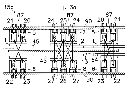
As shown in Figure 5, front sensing assembly 15a comprises a pair of
outer sensing assemblies 1, and an inner sensing assembly 2 positioned
laterally away from and between outer sensing assemblies 1. Each outer
sensing assembly 1 comprises a first photocoupler 5 and a second photocoupler
6 positioned in the vicinity of and on the opposite sides of passageway 13 and
in vertically spaced relation to each other across passageway 13. First
photocoupler 5 has a first light emitting element 20 for emitting a first
light of
first wavelength and a first light receiving element 21 adjacent to first
light
emitting element 20. Likewise, second photocoupler 6 has a second light
emitting element 22 for emitting a second light of second wavelength different
from first wavelength of first light from first light emitting element 20 and
a
second light receiving element 23 adjacent to second light emitting element
22.
First light emitting element 20 is apposed to first light receiving element 21
transversely to the transported direction of bill 64 and in alignment with
second light receiving element 23 across passageway 13. Second light
emitting element 22 is apposed to second light receiving element 23
transversely to the transported direction of bill 64 in alignment with first
light receiving element 21 across passageway 13. First light receiving
element 21 is located in alignment with second light emitting element 22 to
selectively receive first light reflected on bill 64 from first light emitting
element 20 and second light straight penetrating bill 64 from second light
emitting element 22. Second light receiving element 23 is located in
alignment with first light emitting element 20 to selectively receive second
light reflected on bill 64 from second light emitting element 22 and first
light
straight going through bill 64 from first light emitting element 20. First
light emitting element 20 preferably is an infrared ray LED, and second light
CA 02646499 2008-12-04
8
emitting element 22 preferably is an LED for emitting the second light other
than infrared ray, for example red light. In other words, while one of first
and second lights may be an infrared ray, the other of first and second lights
may be of the wavelength other than wavelength of infrared ray. First and
second light emitting elements 20 and 22 are turned on at the different points
in time from each other for time sharing control to prevent simultaneous
reception of first and second lights by first or second light receiving
element
21 or 23.
As demonstrated in Figure 6, rear sensing assembly 15b comprises a
pair of outer sensing assemblies 3 and an inner sensing assembly 4 positioned
laterally away from and between outer sensing assemblies 3. Each outer
sensing assembly 3 comprises a third photocoupler 9 and a fourth
photocoupler 10 positioned in the vicinity of and on the opposite sides of
passageway 13 and in vertically spaced relation to each other across
passageway 13. Third photocoupler 9 has a third light emitting element 30
for emitting a third light and a third light receiving element 31 disposed
adjacent to third light emitting element 30. Likewise, fourth photocoupler
has a fourth light emitting element 32 for emitting a fourth light and a
fourth light receiving element 33 disposed adjacent to fourth light emitting
element 32. Third light emitting element 30 is apposed to third light
receiving element 31 transversely to the transported direction of bill 64 and
in
alignment with fourth light emitting element 32 across passageway 13.
Fourth light emitting element 32 is apposed to fourth light receiving element
33 transversely to the transported direction of bill 64 in alignment with
third
light emitting element 30 across passageway 13. Third light receiving
element 31 is located in alignment with fourth light emitting element 32 to
selectively receive third light reflected on bill 64 from third emitting
element
30 and fourth light straight penetrating bill 64 from fourth light emitting
CA 02646499 2010-09-09
9
element 32. Fourth light receiving element 33 is located in alignment with
third light emitting element 30 to selectively receive fourth light reflected
on
bill 64 from fourth light emitting element 32 and third light straight going
through bill 64 from third light emitting element 30. Fourth light emitting
element 32 preferably is an infrared ray LED, and third light emitting
element 30 preferably is an LED for emitting the fourth light other than
infrared ray, for example green light. In other words, while one of third and
fourth lights may be an infrared ray, the other of third and fourth lights may
be of the wavelength other than wavelength of infrared ray. In any event,
each of first, second, third and fourth lights can be selected from the group
consisting of red, green, yellow, blue and ultraviolet lights and infrared
ray.
Third and fourth light emitting elements 30 and 32 are turned on at the
different points in time from each other for time division control to prevent
the simultaneous reception of the third and fourth lights by third and fourth
light receiving elements 31 and 33.
In the shown embodiment, first and second photocouplers 5 and 6 form
a first fourfold assembly, and third and fourth photocouplers 9 and 10 form a
second fourfold assembly which is arranged longitudinally along passageway
13 behind the first fourfold assembly. Figures 5 and 6 show first, second,
third and fourth triplex or threefold assemblies 7, 8, 11 and 12 each of which
has three optical elements arranged in a line. First and second triplex
assemblies 7 and 8 are positioned in the vicinity of and on the opposite sides
of
passageway 13 and in vertically spaced relation to each other across
passageway 13. First triplex assembly 7 comprises two upper or first light
emitting elements 24 for emitting first lights of the same or different
wavelength from each other, and an upper or first light receiving element 25
positioned between first light emitting elements 24 in a line for receiving
first
and second lights reflected on bill 64 at the different points in time. For
CA 02646499 2008-12-04
example, each of first light emitting elements 24 may be an LED for
generating the same red light. Disposed in alignment with and beneath
first triplex assembly 7 across passageway 13 is a second triplex assembly 8
which comprises two lower or second light receiving elements 27 and a lower
or second light emitting element 26 disposed between two second light
receiving elements 27 in a line for emitting a second light. For example,
first light emitting elements 24 are red LEDs and second light emitting
element 26 is an infrared ray LED. In this arrangement, first light
receiving element 25 can receive first lights reflected on bill 64 from first
light
emitting elements 24 and second light straight penetrating bill 64 from second
light emitting element 26. Each of second light receiving elements 27 can
receive second light reflected on bill 64 from second light emitting element
26
and first light straight going through bill 64 from first light emitting
element
24.
Third triplex assembly 11 comprises two upper or first light emitting
elements 34 for emitting first lights of the same or different wavelength from
each other, and an upper or first light receiving element 35 positioned
between first light emitting elements 34 in a line for receiving first and
second
lights reflected on bill 64 at different points in time. For example, each of
first light emitting elements 34 may be an LED for generating infrared ray.
Disposed in alignment with and beneath third triplex assembly 11 across
passageway 13 is a fourth triplex assembly 12 which comprises to lower or
fourth light receiving elements 37 and a lower or fourth light emitting
element 36 disposed between fourth light receiving elements 37 in a line for
emitting a fourth light. For example, third light emitting elements are
infrared ray LEDs and fourth light emitting element 36 is a green LED. In
this arrangement, third light receiving element 35 can receive third lights
reflected on bill 64 from third light emitting elements 34 and fourth light
CA 02646499 2008-12-04
11
straight penetrating bill 64 from fourth light emitting element 36. Each of
fourth light receiving elements 37 can receive fourth light reflected on bill
64
from fourth light emitting element 36 and third light passing through bill 64
from third light emitting element 34. First, second and third light emitting
elements 24, 26, 34 and 36 are turned on at the different points in time.
These light emitting elements and light receiving elements are LEDs
may preferably be phototransistors, photodiodes or other photoelectric
elements mounted on either of upper and lower printed boards 90 attached in
frame 95. First, second, third and fourth triplex assemblies 7, 8, 11 and 12
are attached along a central axis 13a of passageway 13, and first, second,
third and fourth photocouplers 5, 6, 9 and 10 are attached in the symmetric or
mirror imaged positions with respect to the central axis 13a. A pair of
spacers 45 made of light permeable material such as transparent resin are
positioned between upper and lower light emitting and receiving elements.
For example, spacers 45 may be of an elongated plate or cylindrical lens. As
shown in Figure 7, light emitting elements 20, 30 and light receiving elements
21, 31 are located in an upper case 91 with a partition 87 for keeping light
emitting elements 20, 30 and light receiving elements 21, 31 in an
appropriately spaced relation to each other. Likewise, light emitting
elements 22, 32 and light receiving elements 23, 33 are located in a lower
case
92 with a partition 87 for keeping light emitting elements 22, 32 and light
receiving elements 23, 33 in an appropriately spaced relation to each other.
Light emitting elements 24, 34 and light receiving elements 25, 35 are located
in an upper case 93 together with thread sensor 17 with partitions 87 for
keeping these elements in an appropriately spaced relation to each other.
Similarly, light emitting elements 26, 36 and light receiving elements 27, 37
are located in a lower case 94 together with thread sensor 17 with partitions
87 for keeping these elements in an appropriately spaced relation to each
CA 02646499 2008-12-04
12
other.
As mentioned above, in the first embodiment of the present invention
for combining two light emitting elements and two light receiving elements,
the sensing device comprises a first photocoupler 5 or 9 and a second
photocoupler 6 or 10 disposed in the proximity to and on the opposite sides of
passageway 13. First photocoupler 5 or 9 comprises a first light emitting
element 20 or 30 for emitting a first light, and a first light receiving
element
21 or 31 disposed in the vicinity of first light emitting element 20 or 30.
Second photocoupler 6 or 10 comprises a second light emitting element 22 or
32 for emitting a second light of the light wavelength different from that of
the
first light, and a second light emitting element 23 or 33. First light
receiving element 21 or 31 can receive first light reflected on bill 64 from
first
light emitting element 20 or 30, and second light straight penetrating bill 64
from second light emitting element 22 or 32. Second light receiving element
23 or 33 can receive second light reflected on bill 64 from second light
emitting
element 22 or 32, and first light straight going through bill 64 from first
light
emitting element 20 or 30. Accordingly, combination of first photocoupler 5
or 9 and second photocoupler 6 or 10 can pick up four kinds of optical
features
or patterns of bill 64 inclusive of two penetration light characteristics and
two
reflection light characteristics, reducing the number of light emitting and
receiving elements.
Figures 9 and 10 exemplify another embodiment of a sensing device 18
that has front and rear sensing assemblies 15a, 15b. As shown in Figure 8,
front sensing assembly 15a comprises a pair of outer sensing assemblies 1 and
an inner sensing assembly 2 positioned between and in laterally spaced
relation to outer sensing assemblies 1. Each outer sensing assembly 1
comprises first and second triplex assemblies 72 and 73 positioned adjacent to
CA 02646499 2008-12-04
13
and in vertically spaced relation to each other across passageway 13. First
triplex assembly 72 comprises a first light emitting element 40 for emitting a
first light and a pair of first light receiving elements 41 disposed in the
proximity to first light emitting element 40. Second triplex assembly 73
comprises a pair of second light emitting elements 42 for emitting second
lights and a second light receiving element 43 disposed in the proximity to
and
between second light emitting elements 42. First light emitting element
40 and first light receiving elements 41 are attached to upper printed board
90
in alignment with respectively second light receiving element 43 and second
light emitting elements 42 attached to lower printed board 90 so that each of
first light receiving elements 41 can receive first light reflected on bill 64
from
first light emitting element 40 and second light straight penetrating bill 64
from second light emitting element 42, and second light receiving element 43
can receive first light straight passing through bill 64 from first light
emitting
element 40 and both second lights reflected on bill 64 from two second light
emitting elements 42. For example, first light emitting element 40 may be
an LED of infrared ray, second light emitting elements 42 may be red LEDs,
and light receiving elements may be phototransistors.
Inner sensing assembly 2 comprises first and second triplex assemblies
74 and 75 positioned adjacent to and in vertically spaced relation to each
other across passageway 13. First triplex assembly 74 comprises a first
light emitting element 46 for emitting a first light, and two first light
receiving elements 47 disposed in the proximity to and on the opposite sides
of
first light emitting element 46. Second triplex assembly 75 comprises two
second light emitting elements 48 for emitting second lights and a second
light receiving element 49 disposed in the proximity to and between second
light emitting elements 48. First light emitting element 46 and first light
receiving elements 47 are attached to upper printed board 90 in alignment
CA 02646499 2008-12-04
14
with respectively second light receiving element 49 and second light emitting
elements 48 attached to lower printed board 90 so that each of first light
receiving elements 47 can receive first light reflected on bill 64 from first
light
emitting element 46 and second light straight penetrating bill 64 from second
light emitting element 48, and second light receiving element 49 can receive
first light straight going through bill 64 from first light emitting element
46
and both second lights reflected on bill 64 from two second light emitting
elements 48. For example, first light emitting element 46 may be a red LED
second light emitting elements 48 may be LEDs of infrared ray, and light
receiving elements may be phototransistors.
As shown in Figure 10, rear sensing assembly 15b comprises a pair of
outer sensing assemblies 3 and an inner sensing assembly 4 positioned
between and in laterally spaced relation to outer sensing assemblies 3.
Each outer sensing assembly 3 comprises first and second triplex assemblies
76 and 77 positioned adjacent to and in vertically spaced relation to each
other across passageway 13. First triplex assembly 76 comprises a first
light emitting element 50 for emitting a first light and a pair of first light
receiving elements 51 disposed in the proximity to first light emitting
element
50. Second triplex assembly 77 comprises a pair of second light emitting
elements 53 for emitting second lights and a second light receiving element 54
disposed in the proximity to and between second light emitting elements 53.
First light emitting element 50 and first light receiving elements 51 are
attached to upper printed board 90 in alignment with respectively second
light receiving element 54 and second light emitting elements 53 attached to
lower printed board 90 so that each of first light receiving elements 51 can
receive first light reflected on bill 64 from first light emitting element 50
and
second light straight penetrating bill 64 from second light emitting element
53,
and second light receiving element 54 can receive first light straight going
CA 02646499 2008-12-04
through bill 64 from first light emitting element 50 and both second lights
reflected on bill 64 from two second light emitting elements 53. For
example, first light emitting element 50 may be a green LED, second light
emitting elements 53 may be LEDs of infrared ray, and light receiving
elements may be phototransistors.
Inner sensing assembly 4 comprises first and second triplex assemblies
78 and 79 positioned adjacent to and in vertically spaced relation to each
other across passageway 13. First triplex assembly 78 comprises a first
light emitting element 56 for emitting a first light, and two first light
receiving elements 57 disposed in the proximity to and on the opposite sides
of
first light emitting element 56. Second triplex assembly 79 comprises a pair
of second light emitting elements 58 for emitting second lights and a second
light receiving element 59 disposed in the proximity to and between second
light emitting elements 58. First light emitting element 56 and first light
receiving elements 57 are attached to upper printed board 90 in alignment
with respectively second light receiving element 59 and second light emitting
elements 58 attached to lower printed board 90 so that each of first light
receiving elements 57 can receive first light reflected on bill 64 from first
light
emitting element 56 and second light straight penetrating bill 64 from second
light emitting element 58, and second light receiving element 59 can receive
first light penetrating bill 64 from first light emitting element 56 and both
second lights reflected on bill 64 from two second light emitting elements 58.
For example, first light emitting element 56 may be an LED of infrared ray,
second light emitting elements 58 may be green LEDs, and light receiving
elements may be phototransistors.
As above-mentioned, in the second embodiment of the present
invention, the optical sensing device comprises first triplex assemblies 7,
11,
CA 02646499 2008-12-04
16
72, 74, 76 and 78 and second triplex assemblies 8, 12, 73, 75, 77 and 79, one
of
which comprises a pair of outer light emitting elements 24, 34, 42, 48, 53 and
58 and inner light receiving elements 25, 35, 43, 49, 54 and 59 positioned
between the pair of outer light emitting elements 24, 34, 42, 48, 53 and 58,
and the other of which comprises a pair of outer light receiving elements 27,
37, 41, 47, 51 and 57 and inner light emitting elements 26, 36, 40, 46, 50 and
56 positioned between the pair of outer light receiving elements 27, 37, 41,
47,
51 and 57 for emitting lights of light wavelengths different from those of
outer
light emitting elements 24, 34, 42, 48, 53 and 58.
Inner light receiving elements 25, 35, 43, 49, 54 and 59 can receive
lights reflected on bill 64 from outer light emitting elements 24, 34, 42, 48,
53
and 58, and lights straight penetrating bill 64 from inner light emitting
elements 26, 36, 40, 46, 50 and 56. Each of outer light receiving elements 27,
37, 41, 47, 51 and 57 can receive lights reflected on bill 64 from inner light
emitting elements 26, 36, 40, 46, 50 and 56, and lights straight going through
bill 64 from outer light emitting elements 24, 34, 42, 48, 53 and 58.
Combination of first triplex assemblies 7, 11, 72, 74, 76 and 78 and second
triplex assemblies 8, 12, 73, 75, 77 and 79 can take out seven kinds of
optical
features or patterns of bill 64 inclusive of three penetration light
characteristics and four reflection light characteristics, reducing the number
of light emitting and receiving elements.
A pair of outer light emitting elements 24, 34, 42, 48, 53 and 58 of first
triplex assembly 7, 11, 72, 74, 76 and 78 and an inner light emitting element
26, 36, 40, 46, 50 and 56 of second triplex assembly 8, 12, 73, 75, 77 and 79
can
be selected from the group consisting of LEDs for producing infrared ray and
light of wavelength other than infrared ray. Inner light receiving element
25, 35, 43, 49, 54 and 59 can receive lights reflected on bill 64 from the
pair of
CA 02646499 2008-12-04
17
outer light emitting elements 24, 34, 42, 48, 53 and 58 of first triplex
assembly
7, 11, 72, 74, 76 and 78 and second light straight penetrating bill 64 from
inner light emitting element 26, 36, 40, 46, 50 and 56. The pair of outer
light receiving elements 27, 37, 41, 47, 51 and 57 can receive lights straight
penetrating bill 64 from the pair of outer light emitting elements 24, 34, 42,
48,
53 and 58 of first triplex assembly 7, 11, 72, 74, 76 and 78, and lights
reflected
on bill 64 from inner light emitting element 26, 36, 40, 46, 50 and 56 of
second
triplex assembly 8, 12, 73, 75, 77 and 79.
Light emitting and receiving elements in each triplex assembly are
arranged in a line perpendicular to the direction for moving bill 64. First
triplex assembly 7, 11, 72, 74, 76 and 78 is disposed in a laterally spaced
relation to first photocoupler 5 or 9, and second triplex assembly 8, 12, 73,
75,
77 and 79 is disposed in a laterally spaced relation to second photocoupler 6
or
to form a combined structure of a fourfold assembly that comprises two
light emitting elements and two light receiving elements and a sixfold
assembly that comprises three light emitting elements and three light
receiving elements. Outer light emitting elements 24, 34, 42, 48, 53 and 68
and inner light emitting elements 26, 36, 40, 46, 50 and 56 are turned on at
different points in time from each other for time sharing control to avoid
receiving overlapped lights emitted from different light emitting elements.
As shown in Figure 8, inlet sensor 14, optical sensing device 15,
magnetic sensing device 16 and thread sensor 17 are connected to input
terminals of control device 96 through an amplifier 97, and output terminals
of control device 96 are connected to light emitting elements of sensing
device18 and motor control circuit 68 of conveyor 19 for activating convey
motor 66.
CA 02646499 2008-12-04
18
In operating'the bill validator, a bill 64 is inserted into inlet 60, and
inlet sensor 14 detects insertion of bill 64 to produce a detection signal to
control device 96 that then forwards drive signals to motor control circuit 68
to rotate convey motor 66. Thus, bill 64 is transported by convey belts 39
into and along passageway 13, and sensing device 18 is activated when bill 64
passes sensing device 18. Accordingly, light emitting elements 20, 22, 24,
26, 30, 32, 34, 36, 40, 42, 46, 48, 50, 53, 56 and 58 are turned on if they
are
disposed in the same case 91, 92, 93 and 94 to avoid undesirable optical
interference by simultaneous light emission. Plural optical features of bill
64 are converted into electric signals by light receiving element 21, 23, 25,
27,
31, 33, 35, 37, 41, 43, 47, 49, 51,54, 57 and 59 that receive any light
emitted
from light emitting elements 20, 22, 24, 26, 30, 32, 34, 36, 40, 42, 46, 48,
50, 53,
56 and 58 so that the electric signals are supplied to control device 96.
When infrared ray penetrates bill 64, it can be received by a light receiving
element with less impact by colored ink printed on bill 64 but with impact by
paper quality of bill 64, and therefore, received infrared ray can provide
reference or basic light data for detecting a light amount level of light
other
than infrared ray, such as red, green, yellow, blue or ultraviolet light. In
this case, difference between received light amounts of infrared ray and light
other than infrared ray provides good optical data without influence by paper
quality of bill 64. Control device 96 discriminates authenticity of bill 64 in
view of the received detection signals, and further drives conveyor 19 to
discharge bill 64 to accumulate it in a stacking chamber 44 when control
device 96 determines bill 64 as genuine. Adversely, when control device 96
does not determine bill 64 as genuine, it drives conveyor 19 in the reverse
direction to return bill 64 to inlet 60.
The above-mentioned embodiments of the invention may be varied in
various ways. For example, the optical sensing device may comprise three
CA 02646499 2008-12-04
19
or three pairs of photocouplers in lieu of a pair of first and second
photocouplers 5 and 6 or 9 and 10, or three or three pairs of triplex
assemblies.
As shown in Figure 11, light receiving element 31 can be removed from case
91 with light emitting elements 20, 30 and light receiving element 21
positioned at vertexes of a plane triangle as shown in Figure 12, and light
receiving element 23 can be removed from case 92. Also, light receiving
element 35 can be removed from case 93 as shown in Figure 13, light receiving
element 37 can be removed from case 94 to mount a single light receiving
element 27 and light emitting elements 26 and 36 in case 94 as shown in
Figure 12. Positions and combination of photocouplers and triplex
assemblies can be selected as required. It should be noted that the present
invention can also be applied to valuable papers such as bonds, certificates,
coupons, scrip, currency, banknotes, paper money, tickets other than bills.