Note: Descriptions are shown in the official language in which they were submitted.
CA 02646692 2008-09-19
WO 2007/107973
PCT/1L2006/000364
REDUCED DARK CURRENT PHOTODETECTOR
BACKGROUND OF THE INVENTION
[0001] The
invention relates generally to the field of semiconductor based
photo-detectors and in particular to a photo-detector exhibiting a barrier
region
between an active semiconductor region and a contact semiconductor region.
[0002]
Photo-detectors are used in a wide variety of applications including
imaging. A specific type of photo-detector sensitive to the infra-red
wavelengths of
light is also known as an infra-red detector. Infra-red covers a broad range
of
wavelengths, and many materials are only sensitive to a certain range of
wavelengths.
As a result, the infra-red band is further divided into sub-bands such as near
infra-red
defined conventionally as 0.75 ¨ 1.4 gm; short wavelength infra-red defined
conventionally as 1.3 ¨ 3 gm; mid wavelength infra-red defined conventionally
as 3 ¨
8 gm; and far infra-red defined conventionally as 15 ¨ 1,000 gm. Infra-red in
the
range of 5 gm to 8 gm is not well transmitted in the atmosphere and thus for
many
infra-red detection applications mid-wavelength infra-red is referred to as 3
¨ 5 gm.
[0003]
Infra-red detectors are used in a wide variety of applications, and in
particular in the military field where they are used as thermal detectors in
night vision
equipment, air borne systems, naval systems and missile systems. Highly
accurate
thermal detectors have been produced using InSb and HgCdTe p-n junction
diodes,
however these thermal detectors require cooling to cryogenic temperatures of
around
77 K which is costly. The cryogenic temperatures primarily are used to reduce
the
dark current generated in the p-n junction diode by among other effects
Shockley
Reed Hall (SRH) generation.
[0004]
There are three main contributions to the dark current, denoted as Lark;
of photodiodes based on narrow band gap semiconductors. The fluctuations of
the
dark current components are a major factor in the noise that limits the device
performance. These components are:
a) a generation current associated with the Shockley-Reed-Hall (SRH) process
in
the depletion region, Isrh;
b) a diffusion current associated with auger or radiative processes in the
extrinsic
area, Idiy, and
CA 02646692 2008-09-19
WO 2007/107973
PCT/1L2006/000364
c) a surface current associated with the surface states in the junction,
Isõ,f. The
surface current depends primarily on the passivation process done for the
device.
Thus, Lark can be expressed as:
'dark = srh diff + surf Equation 1
[0005] The SRH generation process is very efficient in the depletion
region of
photodiodes where the mid-gap traps are highly activated. It is the main
source of the
dark current in photodiodes operable for mid-wavelength infrared at
temperatures
below 200K. The current associated with this source is:
ni
Jai/ q Wdep
SRH Equation 2
where ni is the intrinsic concentration of the semiconductor, Wdep is the
depletion
width (typically in the range of lgm), andsrh -8 i the SRH lifetime of
minority carriers
in the extrinsic area. The SRH lifetime of minority carriers in the extrinsic
area
depends on the quality of the material, i.e. the trap concentration, and is
typically in
the range of ¨1p,sec in low doped material (-1016 cm-3). The dependence of SRH
current on ni produces an activation energy of Eg/2 (ni¨exp(-Eg/2/kT)),
because the
source of this generation process is through mid-gap traps. A secondary source
of
dark current in photodiodes is thermal generation in the neutral regions and
diffusion
to the other side of the junction. This thermal generation current depends on
the auger
or radiative process in this area, and is expressed as:
1 ni2 1
J (WI (IP õ X rdiffLx =q¨x¨xL
Nd rdfff Equation 3
where tdiff is the lifetime, and in an n-type material exhibiting a doping
concentration,
denoted Nd, of ¨1-2=1016cm-3 is in the range of ¨ 0.5psec, depending only
slightly on
temperature. L is the width of the neutral region of the device or the
diffusion length
of minority carriers (the smaller of the two) and pn is the hole concentration
in the
active n type semiconductor in equilibrium and it equal to n12/Nd. The
activation
2
CA 02646692 2008-09-19
WO 2007/107973
PCT/1L2006/000364
energy of the diffusion current is Eg, (n? ¨exp(-Eg/kT)) as the process
involves band
to band excitation.
[0006]
Additionally, p-n junction diodes, and particularly those produced for
thermal imaging require a passivation layer in the metallurgic junction
between the p
and n layers. Unfortunately this is often difficult to achieve and
significantly adds to
the cost of production.
[0007]
There is thus a long felt need for a photo-detector having reduced dark
noise. Preferably the photo-detector would be sensitive to the mid wavelength
infra-
red band and not require expensive passivation in production. Further
preferably the
photo-detector would be operable at significantly higher temperatures than
77K.
SUMMARY OF THE INVENTION
[0008]
Accordingly, it is a principal object of the present invention to
overcome the disadvantages of prior art photo-detectors, and in particular mid
wavelength infra-red detectors. This is provided in the present invention by a
photo-
detector sensitive to a target waveband comprising a photo absorbing layer,
preferably
exhibiting a thickness on the order of the optical absorption length. In an
exemplary
embodiment the photo absorbing layer is deposited to a thickness of between
one and
two times the optical absorption length. A contact layer is further provided,
and a
barrier layer is interposed between the photo absorbing layer and the contact
layer.
The barrier layer exhibits a thickness sufficient to prevent tunneling of
majority
carriers from the photo absorbing layer to the contact layer, and a band gap
barrier
sufficient to block the flow of thermalized majority carriers from the photo
absorbing
layer to the contact layer. The barrier layer does not significantly block
minority
carriers.
[0009] An
infra-red detector in accordance with the principle of the invention
can be produced using either an n-doped photo absorbing layer or a p-doped
photo
absorbing layer, in which the barrier layer is designed to have no offset for
minority
carriers and a band gap barrier for majority carriers. Current in the detector
is thus
almost exclusively by minority carriers. In particular, for an n-doped photo
absorbing
layer the junction between the barrier layer and the absorbing layer is such
that there
is substantially zero valence band offset, i.e. the band gap difference
appears almost
exclusively in the conduction band offset. For a p-doped photo absorbing layer
the
junction between the bather layer and the absorbing layer is such that there
is
3
CA 02646692 2008-09-19
WO 2007/107973
PCT/1L2006/000364
substantially zero conduction band offset, i.e. the band gap difference
appears almost
exclusively in the valence band offset.
[0010] Advantageously
the photo-detector of the subject invention does not
exhibit a depletion layer, and thus the dark current is significantly reduced.
Furthermore, in an exemplary embodiment passivation is not required as the
barrier
layer further functions to achieve passivation.
[0011] The invention
provides for a photo-detector comprising: a photo
absorbing layer comprising an n-doped semiconductor exhibiting a valence band
energy level and a conducting band energy level; a barrier layer, a first side
of the
barrier layer adjacent a first side of the photo absorbing layer, the barrier
layer
exhibiting a valence band energy level substantially equal to the valence band
energy
level of the photo absorbing layer and a conduction band energy level
exhibiting a
significant band gap in relation to the conduction band of the photo absorbing
layer;
and a contact area comprising a doped semiconductor, the contact area being
adjacent
a second side of the barrier layer opposing the first side, the barrier layer
exhibiting a
thickness, the thickness and the band gap being sufficient to prevent
tunneling of
majority carriers from the photo absorbing layer to the contact area and block
the flow
of thermalized majority carriers from the photo absorbing layer to the contact
area.
[0012] In one
embodiment the barrier layer comprises an undoped
semiconductor. In another embodiment the contact area is n-doped. In a further
embodiment, the contact area exhibits a valence band energy level
substantially equal
to the valence band energy level of the n-doped semiconductor of the photo
absorbing
layer.
[0013] In one
embodiment the contact area is p-doped. In one further
embodiment the contact area exhibits a valence band energy level greater than
the
valence band energy level of the n-doped semiconductor of the photo absorbing
layer.
In another further embodiment the barrier layer comprises an undoped
semiconductor.
[0014] In one
embodiment the photo absorbing layer is operable to generate
minority carriers in the presence of light energy exhibiting a wavelength of 3
¨ 5
microns. In another embodiment the photo-detector further comprises a
substrate
exhibiting a first side adjacent a second side of the photo absorbing layer,
the second
side of the photo absorbing layer opposing the first side of the photo
absorbing layer,
the substrate exhibiting a second side in contact with a metal layer.
Preferably, the
4
CA 02646692 2008-09-19
WO 2007/107973
PCT/1L2006/000364
photo-detector further comprises an additional metal layer in contact with the
contact
area.
[0015] In one embodiment the barrier layer comprises one of AlSb,
AlAsSb,
GaAlAsSb, AlPSb, AlGaPSb and HgZnTe. In a further embodiment the photo
absorbing layer is constituted of one of n-doped InAs, n-doped InAsSb, n-doped
InGaAs, n-doped Type II super lattice InAs/InGaSb and n-doped HgCdTe. In a yet
further embodiment the contact area is constituted of one of InAs, InGaAs,
InAsSb,
Type II super lattice InAs/InGaSb, HgCdTe and GaSb. In a yet further
embodiment
the contact area and the photo absorbing layer exhibit substantially identical
compositions.
[0016] In one embodiment the photo absorbing layer and the contact
area are
constituted of n-doped HgCdTe and the barrier layer is constituted of HgZnTe,
and in
another embodiment the photo absorbing layer and the contact layer are
constituted of
n-doped type II super lattice InAs/InGaSb and the barrier layer is constituted
of
AlGaAsSb. In another embodiment the photo absorbing layer is constituted of n-
doped InAsSb, the barrier layer is constituted of AlGaAsSb and the contact
layer is
constituted of p-doped GaSb. In one embodiment the photo absorbing layer
exhibits a
thickness on the order of the optical absorption length.
[0017] The invention independently provides for a photo-detector
comprising:
a photo absorbing layer comprising a p-doped semiconductor exhibiting a
conduction
band energy level and a valence band energy level; a barrier layer, a first
side of the
barrier layer adjacent a first side of the photo absorbing layer, the barrier
layer
exhibiting a conduction band energy level substantially equal to the
conduction band
energy level of the photo absorbing layer and a valence band energy level
exhibiting a
significant band gap in relation to the valence band of the photo absorbing
layer; and a
contact area comprising a doped semiconductor, the contact area adjacent a
second
side of the barrier layer opposing the first side, the barrier layer
exhibiting a thickness,
the thickness and the band gap being sufficient to prevent tunneling of
majority
carriers from the photo absorbing layer to the contact area and to block the
flow of
thermalized majority carriers from the photo absorbing layer to the contact
area.
[0018] In one embodiment the barrier layer comprises an undoped
semiconductor. In another embodiment the contact area is p-doped. In one
further
embodiment the contact area exhibits a conduction band energy level
substantially
5
CA 02646692 2008-09-19
WO 2007/107973
PCT/1L2006/000364
equal to the conduction band energy level of the p-doped semiconductor of the
photo
absorbing layer.
[0019] In one embodiment the contact area is n-doped. In one further
embodiment the c ontact area exhibits a c onduction b and energy level less
than the
conduction band energy level of the p-doped semiconductor of the photo
absorbing
layer. In another further embodiment the barrier layer comprises an undoped
semiconductor.
[0020] In one embodiment the photo absorbing layer is operable to
generate
minority carriers in the presence of light energy exhibiting a wavelength of 3
¨ 5
microns. In another embodiment the photo-detector further comprises a
substrate
exhibiting a first side adjacent a second side of the photo absorbing layer,
the second
side of the photo absorbing layer opposing the first side of the photo
absorbing layer,
the substrate exhibiting a second side in contact with a metal layer. In a
further
embodiment the photo-detector further comprises a metal layer in contact with
the
contact area.
[0021] In one embodiment the barrier layer comprises one of AlSb,
AlAsSb,
GaAlAsSb, AlPSb, AlGaPSb, InAlAs, InAlAsSb, and HgZnTe. In one further
embodiment the photo absorbing layer is constituted of one of p-doped InAs, p-
doped
InAsSb, p-doped InGaAs, p-doped Type II super lattice InAs/InGaSb and p-doped
HgCdTe. In one yet further embodiment the contact area is constituted of one
of
InAs, InGaAs, InAsSb, Type II super lattice InAs/InGaSb, HgCdTe and GaSb. In
one
yet further embodiment the contact area and the photo absorbing layer exhibit
substantially identical compositions.
[0022] The invention independently provides for a method of producing
a
photo-detector, the method comprising: providing a substrate; depositing on
the
substrate a photo absorbing layer comprising a doped semiconductor exhibiting
an
energy level associated with non-conducting majority carriers; depositing on
the
deposited photo absorbing layer a barrier layer exhibiting a thickness, an
energy level
associated with minority carriers of the photo absorbing layer substantially
equal to
the energy level of the photo absorbing layer and a band gap associated with
majority
carriers of the photo absorbing layer; and depositing on the deposited barrier
layer a
contact layer comprising a doped semiconductor, the thickness and the band gap
of
the b arrier layer being sufficient to prevent tunneling o fm ajority carriers
from the
6
CA 02646692 2009-03-02
photo absorbing layer to the contact layer and to block the flow of
thermalized
majority carriers from the photo absorbing layer to the contact layer.
100231 In one embodiment the method further comprises selectively
etching
the deposited contact layer to define a plurality of contact areas. In another
embodiment at least one of depositing the photo absorbing layer, depositing
the barrier
layer and depositing the contact layer is done via one of molecular beam
epitaxy,
metal organic chemical vapor deposition, metal organic phase epitaxy and
liquid phase
epitaxy.
Accordingly, in one aspect the present invention resides in a photo-
detector comprising a first layer comprising a doped semiconductor exhibiting
a
valence band energy and a conduction band energy; a barrier layer comprising a
semiconductor exhibiting a valence band energy and a conduction band energy, a
first
side of said barrier layer adjacent a first side of said first layer; and a
second layer
comprising a doped semiconductor exhibiting a valence band energy and a
conduction
band energy, said second layer being adjacent a second side of said barrier
layer
opposing said first side, wherein during operation of the photo-detector the
respective
valence band energy and conduction band energy of the first layer, the barrier
layer,
and the second layer allow the flow of photo-generated minority carriers and
substantially block the flow of majority carriers between the first layer and
the second
layer, and wherein during operation said barrier layer functions to achieve
passivation
of the photo-detector.
[0024] Additional features and advantages of the invention will become
apparent from the following drawings and description.
BRIEF DESCRIPTION OF THE DRAWINGS
100251 For a better understanding of the invention and to show how the
same
may be carried into effect, reference will now be made, purely by way of
example, to
the accompanying drawings in which like numerals designate corresponding
elements
or sections throughout.
[0026] With specific reference now to the drawings in detail, it is
stressed that
the particulars shown are by way of example and for purposes of illustrative
discussion of the preferred embodiments of the present invention only, and are
presented in the cause of providing what is believed to be the most useful and
readily
understood description of the principles and conceptual aspects of the
invention. In
7
CA 02646692 2009-03-02
this regard, no attempt is made to show structural details of the invention in
more
detail than is necessary for a fundamental understanding of the invention, the
description taken with the drawings making apparent to those skilled in the
art how
the several forms of the invention may be embodied in practice. In the
accompanying
drawings:
[0027] Fig. IA illustrates a high level schematic view of the layers
of a single
photo-detector according to an embodiment of the principle of the invention;
[0028] Fig. 1B illustrates a side view of a multi-pixel photo-detector
according
to an embodiment of the principle of the invention;
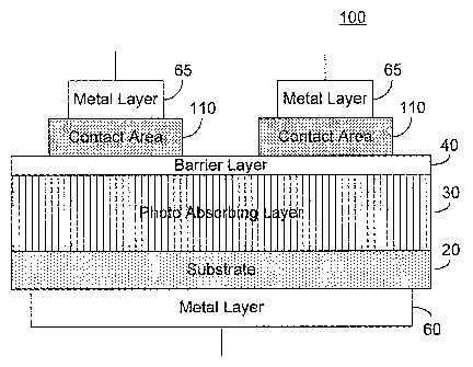
[0029] Fig. 1C illustrates a top level view of the multi-pixel photo-
detector of
Fig. 1B according to a principle of the invention;
7a
CA 02646692 2008-09-19
WO 2007/107973
PCT/1L2006/000364
[0030] Fig. 2A illustrates the energy band levels of an embodiment of
the
structure of Fig. 1 according to the principle of the invention in which the
photo
absorbing layer is n-doped and the contact layer is n-doped;
[0031] Fig. 2B illustrates the energy band levels of an embodiment of
the
structure of Fig. 1 according to the principle of the invention in which the
photo
absorbing layer is p-doped and the contact layer is p-doped;
[0032] Fig. 3A illustrates the energy band levels of an embodiment of
the
structure of Fig. 1 according to the principle of the invention in which the
photo
absorbing layer is n-doped and the contact layer is p-doped;
[0033] Fig. 3B illustrates the energy band levels of an embodiment of the
structure of Fig. 1 according to the principle of the invention in which the
photo
absorbing layer is p-doped and the contact layer is n-doped; and
[0034] Fig 4 illustrates a high level flow chart of the process of
manufacture
of the multi pixel photo-detector of Figs. 1B ¨ 1C.
DETAILED DESCRIPTION OF THE PREFERRED EMBODIMENTS
[0035] The present embodiments enable a photo-detector sensitive to a
target
waveband comprising a photo absorbing layer, preferably exhibiting a thickness
on
the order of an optical absorption length of the target waveband. In an
exemplary
embodiment the photo absorbing layer is deposited to a thickness of between
one and
two times the optical absorption length. A contact layer is further provided,
and a
barrier layer is interposed between the photo absorbing layer and the contact
layer.
The barrier layer exhibits a thickness sufficient to prevent tunneling of
majority
carriers from the photo absorbing layer to the contact layer, and a band gap
barrier
sufficient to block the flow of thermalized majority carriers from the photo
absorbing
layer to the contact layer. The barrier layer does not significantly block
minority
carriers.
[0036] An infra-red detector in accordance with the principle of the
invention
can be produced using either an n-doped photo absorbing layer or a p-doped
photo
absorbing layer, in which the barrier layer is designed to have substantially
no offset
for minority carriers and a band gap barrier for majority carriers. Current in
the
detector is thus almost exclusively by minority carriers. In particular, for
an n-doped
photo absorbing layer the junction between the barrier layer and the absorbing
layer is
8
CA 02646692 2008-09-19
WO 2007/107973
PCT/1L2006/000364
such that there is substantially zero valence band offset, i.e. the band gap
difference
appears almost exclusively in the conduction band offset. For a p-doped photo
absorbing layer the junction between the barrier layer and the absorbing layer
is such
that there is substantially zero conduction band offset, i.e. the band gap
difference
appears almost exclusively in the valence band offset.
[0037]
Advantageously the photo-detector of the subject invention does not
exhibit a depletion layer, and thus the dark current is significantly reduced.
Furthermore, in an exemplary embodiment passivation is not required as the
barrier
layer further functions to achieve passivation.
[0038] Before explaining at least one embodiment of the invention in
detail, it
is to be understood that the invention is not limited in its application to
the details of
construction and the arrangement of the components set forth in the following
description or illustrated in the drawings. The invention is applicable to
other
embodiments or of being practiced or carried out in various ways. Also, it is
to be
understood that the phraseology and terminology employed herein is for the
purpose
of description and should not be regarded as limiting.
[0039] Fig.
lA illustrates a high level schematic view of the layers of a photo-
detector 10 according to an embodiment of the principle of the invention
comprising a
substrate 20, a photo absorbing layer 30, a barrier layer 40, a contact layer
50, a metal
layer 60 and a metal layer 65. Substrate 20 is provided as a base for
deposition and
has deposited on one face metal layer 60 for connection to electronic
circuitry. In an
exemplary embodiment metal layer 60 is constituted of gold. Photo absorbing
layer
is deposited on the second face of substrate 20 opposing the first face. Photo
absorbing layer 30 comprises a doped semiconductor responsive to photons of
the
25 object wavelength, and preferably is deposited to a thickness on the
order of an optical
absorption length. In one embodiment photo absorbing layer 30 is deposited to
a
thickness of between one and two times the optical absorption length. In an
exemplary embodiment photo absorbing layer 30 comprises one of n-doped InAs;
ii-
doped InAsSb; n-doped InGaAs; n-doped type II super lattice of the type
30
InAs/InGaSb; and n-doped HgCdTe. In an alternative embodiment absorbing layer
30 comprises one of p-doped InAs; p-doped InAsSb; p-doped InGaAs; p-doped type
II super lattice of the type InAs/InGaSb; and p-doped HgCdTe.
[0040]
Barrier layer 40 is deposited directly on photo absorbing layer 30
without requiring passivation. Barrier layer 40 is deposited to a thickness
sufficient to
9
CA 02646692 2008-09-19
WO 2007/107973
PCT/1L2006/000364
substantially prevent tunneling of majority carriers from photo absorbing
layer 30 to
contact layer 50, and in an exemplary embodiment is deposited to a thickness
of 50 ¨
100 nm. Barrier layer 40 comprises a material selected to exhibit a high band
gap
barrier for majority carriers from photo absorbing layer 30 and substantially
no band
gap barrier for minority carriers, Barrier layer 40 is thus sufficient to
block both the
flow of thermalized majority carriers and the tunneling of majority carriers
from
photo absorbing layer 30 to contact layer 50. Thus, for an n-type photo
absorbing
layer 30, the band gap difference appears in the conduction band, whereas
substantially no band gap offset appears in the valence band. In one
embodiment
barrier layer 40 comprises one of AlSb, AlAsSb, GaAlAsSb, AlPSb, AlGaF'Sb and
HgZnTe. In an exemplary embodiment photo absorbing layer 30 comprises n-doped
InAs and barrier layer 40 is comprised of AlAsõSbi, with x-0.15, and thus
there is ¨0
valence band offset.
[0041] Contact layer 50 is deposited on barrier layer 40. Contact
layer 50
functions to absorb the minority carriers diffused from the absorbing layer 30
and is
essentially a contact layer. In an exemplary embodiment contact layer 50 is
deposited
to a thickness of 20 ¨ 50 nm and is constituted of one of InAs; InAsSb;
InGaAs; type
II super lattice of the type InAs/InGaSb; HgCdTe and GaSb. Contact layer 50
may be
n-doped or p-doped without exceeding the scope of the invention.
Advantageously,
contact layer 50 may be constituted of the same material as photo absorbing
layer 30.
Contact layer 50 is etched, preferably by photolithography, to define the
detector area.
Advantageously etching of barrier layer 40 or absorbing layer 30 is not
required.
Metal layer 65 is deposited on contact layer 50, and in an exemplary
embodiment is
constituted of gold. Metal layers 60, 65 enable the connection of an
appropriate bias,
and a connection to detect a flow of current from photo absorbing layer 30 to
contact
layer 50.
[0042] Fig. 1B illustrates a side view of a multi-pixel photo-
detector 100
according to an embodiment of the principle of the invention comprising
substrate 20,
photo absorbing layer 30, barrier layer 40, a first and second contact area
110, a metal
layer 6 and a metal layer 65. Substrate 20 is provided as a base for
deposition and has
deposited on one face metal layer 60 for connection to electronic circuitry.
In an
exemplary embodiment metal layer 60 is constituted of gold. Photo absorbing
layer
30 is deposited on the second face of substrate 20 opposing the first face.
Photo
absorbing layer 30 comprises a doped semiconductor responsive to photons of
the
CA 02646692 2008-09-19
WO 2007/107973
PCT/1L2006/000364
object wavelength, and preferably is deposited to a thickness on the order of
an optical
absorption length. In one embodiment photo absorbing layer 30 is deposited to
between one and two times the optical absorption length. In an exemplary
embodiment photo absorbing layer 30 comprises one of n-doped InAs; n-doped
InAsSb; n-doped InGaAs; n-doped type II super lattice of the type InAs/InGaSb;
and
n-doped HgCdTe. In an alternative embodiment absorbing layer 30 comprises one
of
p-doped InAs; p-doped InAsSb; p-doped InGaAs; p-doped type II super lattice of
the
type InAs/InGaSb; and p-doped HgCdTe.
[0043] Barrier layer 40 is deposited directly on photo absorbing
layer 30
without requiring passivation. Barrier layer 40 is deposited to a thickness
sufficient to
substantially prevent tunneling of majority carriers from photo absorbing
layer 30 to
first and second contact area 110, and in an exemplary embodiment is deposited
to a
thickness of 50 - 100 nm. Barrier layer 40 comprises a material selected to
exhibit a
high band gap barrier for majority carriers from photo absorbing layer 30 and
substantially no band gap barrier for minority carriers. Barrier layer 40 is
thus
sufficient to block both the flow of thermalized majority carriers and the
tunneling of
majority carriers from photo absorbing layer 30 to first and second contact
area 110.
Thus, for an n-type photo absorbing layer 30, the band gap difference appears
in the
conduction band, whereas substantially no band gap offset appears in the
valence
band. In one embodiment barrier layer 40 comprises one of AlSb, AlAsSb,
GaAlAsSb, AlPSb, AlGaPSb and HgZnTe. In an exemplary embodiment photo
absorbing layer 30 comprises n-doped InAs and barrier layer 40 is comprised of
AlAsõSbi, with x-0.15, and thus there is -0 valence band offset.
[0044] Contact layer 50 as described above in relation to Fig. lA is
deposited
on barrier layer 40. Contact layer 50, which as will be described further is
etched to
define first and second contact area 110, functions to absorb the minority
carriers
diffused from the absorbing layer 30 and is essentially a contact layer. In an
exemplary embodiment contact layer 50 is deposited to a thickness of 20 - 50
rim and
is constituted of one of InAs; InAsSb; InGaAs; type II super lattice of the
type
hiAs/InGaSb; HgCdTe and GaSb. Contact layer 50 may be n-doped or p-doped
without exceeding the scope of the invention. Advantageously, contact layer 50
may
be constituted of the same material as photo absorbing layer 30. Contact layer
50 is
etched, preferably by photolithography, to define first and second contact
area 110.
Advantageously etching of barrier layer 40 or absorbing layer 30 is not
required. In
11
CA 02646692 2008-09-19
WO 2007/107973
PCT/1L2006/000364
an exemplary embodiment a selective etchant is used which does not etch
barrier layer
40. Metal layer 65 is deposited on each of first and second contact area 110,
and in an
exemplary embodiment is constituted of gold. Thus, a single photo absorbing
layer
and barrier layer is utilized, with each unetched portion of contact layer 50
defining a
pixel or individual detector.
[0045] The above has been described in an embodiment in which two
pixels,
or detectors are defined, however this is not meant to be limiting in any way.
A large
array of photo-detectors produced as above is specifically included in the
invention.
[0046] Fig. 1C illustrates a top level view of multi-pixel photo-
detector 100 of
Fig. 1B according to a principle of the invention showing barrier layer 40,
first and
second contact area 110 and metal layer 65 defined on each of first and second
contact
area 110.
[0047] Fig. 2A illustrates the energy band levels of an embodiment of
the
structure of Fig. 1 according to the principle of the invention in which the
photo
absorbing layer is n-doped and the contact layer is n-doped, in which the x-
axis
indicates position along the structure of Fig. 1 and the y-axis indicates
energy levels in
an arbitrary illustrative manner. Three energy band levels are depicted: Eõ,
the
valence band energy band level; Ef, the Fermi energy band level; and Ec the
conducting band energy level. Area 100 represents the energy band levels
within
photo absorbing layer 30, area 110 represents the energy band levels within
barrier
layer 40 and area 120 represent the energy band levels within contact layer
50.
[0048] The valence band energy level is substantially constant
throughout
areas 100, 110 and 120, and thus minority carriers are not obstructed from
flowing
from photo absorbing area 100 to contact area 120. It is to be noted that due
to the
energy levels the minority carriers are captured in contact area 120. Bather
layer 40,
represented by area 110, is thick enough so that there is negligible tunneling
of
majority carriers through it. In an exemplary embodiment barrier layer 40 is
deposited to a thickness of 50 - 100 nm, and the band gap bather of area 110
is high
enough so that there is negligible thermal excitation of majority carriers
over it. Area
120 shows energy band levels on a par with that of area 100 however this is
not meant
to be limiting in any way. In one embodiment Ef in contact layer area 120 is
slightly
higher than their values in photo absorbing area 100 with the increase being
attributed
to an increased doping concentration. It is to be noted that no depletion
layer is
present and therefore there is no SRH current. Photocurrent is a result of
optically
12
CA 02646692 2008-09-19
WO 2007/107973
PCT/1L2006/000364
generated minority carriers which diffuse from photo absorbing area 100 to
contact
area 120.
[0049] Fig. 2B illustrates the energy band levels of an embodiment of
the
structure of Fig. 1 according to the principle of the invention in which the
photo
absorbing layer is p-doped and the contact layer is p-doped; in which the x-
axis
indicates position along the structure of Fig. 1 and the y-axis indicates
energy levels in
an arbitrary illustrative manner. Three energy band levels are depicted: Eõ
the
valence band energy level; Ef, the Fermi energy band level; and. Ec the
conducting
band energy level. Area 150 represents the energy band levels within photo
absorbing
layer 30, area 160 represents the energy band levels within barrier layer 40
and area
170 represent the energy band levels within contact layer 50.
[0050] The conduction band energy level is substantially constant
throughout
areas 150, 160 and 170, and thus minority carriers are not obstructed from
flowing
from photo absorbing area 150 to contact area 170. It is to be noted that due
to the
energy levels the minority carriers are captured in contact area 170. Barrier
layer 40,
represented by area 160, is thick enough so that there is negligible tunneling
of
majority carriers through it. In an exemplary embodiment barrier layer 40 is
deposited to a thickness of 50 - 100 nm, and the band gap barrier of area 160
is high
enough so that there is negligible thermal excitation of majority carriers
over it. Area
170 shows energy band levels on a par with that of area 150 however this is
not meant
to be limiting in any way. In one embodiment Ef in contact layer area 170 is
slightly
higher than their values in photo absorbing area 150 with the increase being
attributed
to an increased doping concentration. It is to be noted that no depletion
layer is
present and therefore there is no SRH current. Photocurrent is a result of
optically
generated minority carriers which diffuse from photo absorbing area 150 to
contact
area 170.
[0051] Fig. 3A illustrates the energy band levels of an embodiment of
the
structure of Fig. 1 according to the principle of the invention in which the
photo
absorbing layer is n-doped and the contact layer is p-doped; in which the x-
axis
indicates position along the structure of Fig. 1 and the y-axis indicates
energy levels in
an arbitrary illustrative manner. Three energy band levels are depicted: E,
the
valence band energy level; Ef-, the Fermi energy band level; and Ec the
conducting
band energy level. Area 200 represents the energy band levels within photo
absorbing
13
CA 02646692 2008-09-19
WO 2007/107973
PCT/1L2006/000364
layer 30, area 210 represents the energy band levels within barrier layer 40
and area
220 represent the energy band levels within contact layer 50.
[0052] The valence band energy level is substantially constant
throughout
areas 200 and 210 and is higher in area 220, and thus minority carriers are
not
obstructed from flowing from photo absorbing area 200 to contact area 220. It
is to be
noted that due to the energy levels the minority carriers are captured in
contact area
220. Barrier layer 40, represented by area 210, is thick enough so that there
is
negligible tunneling of majority carriers through it. In an exemplary
embodiment
barrier layer 40 is deposited to a thickness of 50 - 100 nm, and the band gap
barrier of
area 210 is high enough so that there is negligible thermal excitation of
majority
carriers over it. It is to be noted that no depletion layer is present and
therefore there
is no SRH current. Photocurrent is a result of optically generated minority
carriers
which diffuse from photo absorbing area 200 to contact area 220.
[0053] Fig. 3B illustrates the energy band levels of an embodiment of
the
structure of Fig. 1 according to the principle of the invention in which the
photo
absorbing layer is p-doped and the contact layer is n-doped; in which the x-
axis
indicates position along the structure of Fig. 1 and the y-axis indicates
energy levels in
an arbitrary illustrative manner. Three energy band levels are depicted: Ev,
the
valence band energy level; Ef, the Fermi energy band level; and Ec the
conducting
band energy level. Area 250 represents the energy band levels within photo
absorbing
layer 30, area 260 represents the energy band levels within barrier layer 40
and area
270 represent the energy band levels within contact layer 50.
[0054] The conduction band energy level is substantially constant
throughout
areas 250 and 260 and it is lower in area 270, and thus minority carriers are
not
obstructed from flowing from the photo absorbing area 250 to contact area 270.
It is
to be noted that due to the energy levels the minority carriers are captured
in contact
area 270. Barrier layer 40, represented by area 260, is thick enough so that
there is
negligible tunneling of majority carriers through it. In an exemplary
embodiment
barrier layer 40 is deposited to a thickness of 50 - 100 um, and the band gap
barrier of
area 260 is high enough so that there is negligible thermal excitation of
majority
carriers over it. It is to be noted that no depletion layer is present and
therefore there
is no SRH current. Photocurrent is a result of optically generated minority
carriers
which diffuse from photo absorbing area 250 to contact area 270.
14
CA 02646692 2008-09-19
WO 2007/107973
PCT/1L2006/000364
[0055] Fig 4
illustrates a high level flow chart of the process of manufacture
of the photo-detector of Fig. 1. In stage 1000 a substrate material is
provided as a
support for deposition. In stage 1 010, a photo absorbing layer is deposited
on the
substrate. Preferably the photo absorbing layer is deposited to a thickness on
the
order of the optical absorption length and in an exemplary embodiment is
deposited to
a thickness of between one and two times the optical absorption length.
[0056] In
stage 1020, a barrier material is selected such that the flow of
thermalized majority carriers from the photo absorbing layer deposited in
stage 1010
would be negligible, and the flow of minority carriers is not impeded. In
stage 1030,
the barrier material selected in stage 1020 is deposited to a thickness
sufficient to
prevent tunneling of majority carriers through the barrier material. In an
exemplary
embodiment the thickness is between 50 and 100 nm. Preferably the barrier
material
is deposited directly on the photo absorbing layer deposited in stage 1010.
[0057] In
stage 1040, a contact layer is deposited, preferably directly on the
barrier material deposited in stage 1030. In stage 1050, the desired contact
areas are
defined. Preferably, the contact areas are defined by photolithography and a
selective
etchant which stops on the top of the barrier layer. Alternatively, the
etchant may be
controlled to stop once the uncovered portions of contact layer 50 are
removed. Thus,
the depth of the etch is equivalent to the thickness of the contact layer 50.
Advantageously, in an exemplary embodiment no other layer is etched.
[0058] In
stage 1060 a metal layer is deposited on the contact areas defined in
stage 1050 so as to enable electrical connection. Preferably the metal layer
is
deposited directly on the contact areas defined in stage 1050. In stage 1070,
a metal
layer is deposited on substrate 20 provided in stage 1000 so as to enable
electrical
connection.
[0059]
Deposition of the photo absorbing layer of stage 1010, the barrier layer
of stage 1030 and the contact layer of stage 1040 may be accomplished by any
means
known to those skilled in the art including, without limitation molecular beam
epitaxy, metal organic chemical vapor deposition, metal organic phase epitaxy
or
liquid phase epitaxy.
[0060] Thus
the present embodiment enable a photo-detector sensitive to a
target waveband comprising a photo absorbing layer, preferably exhibiting a
thickness
on the order of the optical absorption length. In an exemplary embodiment the
photo
absorbing layer is deposited to a thickness of between one and two times the
optical
CA 02646692 2012-04-19
absorption length. A contact layer is further provided, and a barrier layer is
interposed between the photo absorbing layer and the contact layer. The
barrier layer
exhibits a thickness sufficient to prevent tunneling of majority carriers from
the photo
absorbing layer to the contact layer, and a band gap barrier sufficient to
block the flow
of thermalized majority carriers from the photo absorbing layer to the contact
layer.
The barrier layer does not block minority carriers.
[0061] An infra-red detector in accordance with the principle of the
invention
can be produced using either an n-doped photo absorbing layer or a p-doped
photo
absorbing layer, in which the barrier layer is designed to have no offset for
minority
carriers and a band gap barrier for majority carriers. Current in the detector
is thus
almost exclusively by minority carriers. In particular, for an n-doped photo
absorbing
layer the junction between the barrier layer and the absorbing layer is such
that there is
substantially zero valence band offset, i.e. the band gap difference appears
almost
exclusively in the conduction band offset. For a p-doped photo absorbing layer
the
junction between the barrier layer and the absorbing layer is such that there
is
substantially zero conduction band offset, i.e. the band gap difference
appears almost
exclusively in the valence band offset.
[0062] Advantageously the photo-detector of the subject invention
does not
exhibit a depletion layer, and thus the dark current is significantly reduced.
Furthermore, in an exemplary embodiment passivation is not required as the
barrier
layer further functions to achieve passivation.
[0063] It is appreciated that certain features of the invention,
which are, for
clarity, described in the context of separate embodiments, may also be
provided in
combination in a single embodiment. Conversely, various features of the
invention
which are, for brevity, described in the context of a single embodiment, may
also be
provided separately or in any suitable sub-combination.
[0064] Unless otherwise defined, all technical and scientific terms
used herein
have the same meanings as are commonly understood by one of ordinary skill in
the
art to which this invention belongs. Although methods similar or equivalent to
those
described herein can be used in the practice or testing of the present
invention, suitable
methods are described herein.
[0065] It will be appreciated by persons skilled in the art that the
present
invention is not limited to what has been particularly shown and described
hereinabove. Rather the scope of the present invention is defined by the
appended
16
CA 02646692 2012-04-19
claims and includes both combinations and sub-combinations of the various
features
described hereinabove as well as variations and modifications thereof, which
would
occur to persons skilled in the art upon reading the foregoing description.
17