Note: Descriptions are shown in the official language in which they were submitted.
CA 02646840 2008-12-17
A FREQUENCY AGILE ANTENNA SYSTEM AND METHOD
Field of the Invention
[0001] The field of the invention relates to antenna systems and, more
specifically, to
frequency agile antenna systems that are used to transmit and receive
communications.
Background
[0002] Different types of moveable barrier operators have been sold over
the years
and these barrier operator systems have been used to actuate various types of
moveable
barriers. For example, garage door operators have been used to move garage
doors and gate
operators have been used to open and close gates.
[0003] Such barrier movement operators may include various mechanisms to
facilitate this opening and closing of the barrier. For instance, a wall
control unit may be
coupled to the barrier movement operator and send signals to a head unit
thereby causing the
head unit to open and close the barrier. In addition, operators often include
a receiver unit at
the head unit to receive wireless transmissions from a hand-held code
transmitter or from a
keypad transmitter, which may be affixed to the outside of the area barred by
the barrier or
other structure.
[0004] In previous barrier operator systems, a transmitter (either portable
or
positioned at a fixed location) was used to actuate a moveable barrier
operator and thereby
move the barrier. Some of these transmitters functioned as universal
transmitters in that they
had the ability to transmit signals at several different frequencies.
Generally, these previous
universal transmitters used multiple tuned circuits to produce the different
frequencies. Some
of these previous universal transmitters also utilized mechanical switches in
order to switch
between the different transmitter circuits. Others of these previous systems
used a single
tuned circuit to produce the desired frequencies.
[0005] Unfortunately, all of the above-mentioned previous universal
transmitter
systems suffered from problems. For instance, the multi-circuit transmitters
were usually
expensive to produce because of the need for and use of multiple transmitter
circuits.
Additionally, previous single-tuned circuits were not very efficient in
operation since they
were typically low Q-value circuits and, consequently, could not efficiently
cover the entire
CA 02646840 2008-12-17
spectrum of frequencies needed by the transmitter, especially when the
transmitter was a
small, low-power, handheld transmitter. Other previous systems utilized a
bulky metal loop
antenna, which added undesirable bulk and weight to the transmitter.
Summary
[0006] Universal transmitters are provided for use in moveable barrier
operators
systems. The approaches provided herein provide a transmitter sending
transmissions that
can be made across an adequately wide frequency range, for example, across the
300-434
MHz frequency spectrum used in many moveable barrier operator systems utilize
a single,
tuned circuit that provides adequate Q-values. Additionally, the transmitters
that utilize
these approaches are small, light weight, low power, portable, and can be
powered by a
conventional battery.
[0007] In many of these embodiments, a first value of an operational center
frequency
of a signal to transmit is determined according to received user input. The
operational center
frequency is centered within a first band of frequencies and the first band of
frequencies has a
first bandwidth. A single loop antenna is tuned to match the first value of
the operational
center frequency and the single loop antenna operates across a second band of
frequencies
having a second bandwidth. In many of these examples, the first bandwidth is
less than the
second bandwidth.
[0008] The signal is transmitted from the single loop antenna according to
the first
value of the operational center frequency and received, in one example, at a
moveable barrier
operator. The first value of the operational center frequency may thereafter
be changed to be
a second value and this second value, in many of these approaches, falls
within the second
band of frequencies.
[0009] The tuning of the antenna can be accomplished utilizing a variety of
different
approaches. In one example, the tuning of the antenna is accomplished using a
lookup table.
In another example, the power of the transmitted signal is measured and the
tuning is
accomplished according to the measured power. In still another example,
dampening of the
transmitted signal is determined and the antenna is tuned according to the
dampening. Other
- 2 -
CA 02646840 2008-12-17
examples of tuning are possible and can be made according to other factors or
other
combinations of factors.
100101 In many of these approaches, the Q-value of the system is of an
adequately
high value. Consequently, the transmissions from the antenna can be made
across an entire
spectrum of frequencies while still maintaining the small size of the
transmitter. To take one
example, in many of these approaches, the Q-value is greater than
approximately 10. Other
circuit configurations having other Q-values may be provided.
[0011] As mentioned, transmissions can be made at various center
frequencies and
across a wide variety of bandwidth ranges according to the present approaches.
In one
example, the first bandwidth of transmitted signal is less than approximately
1 Mhz and the
second bandwidth is approximately 10 Mhz. Other examples of center frequencies
and
bandwidths ranges for the transmitted signal are possible.
[0012] In others of these embodiments, a transmitter includes a controller,
a
synthesizer, single loop antenna, and tuner. The controller determines the
operational center
frequency from the received user input. The synthesizer is configured and
arranged to form a
signal to transmit according to received user input. The operational center
frequency is
centered within a first band of frequencies and the first band of frequencies
has a first
bandwidth. The single loop antenna operates across a second band of
frequencies having a
second bandwidth and the first bandwidth is less than the second bandwidth.
The tuner is
coupled to the single loop antenna, the synthesizer, and the controller. The
tuner is
configured and arranged to tune the single loop antenna to the value of the
resonant center
frequency as determined by the synthesizer and as directed by the controller.
[0013] The tuner may include various elements. In one example, the tuner
includes a
varactor. In some of these approaches, a voltage is applied to the varactor to
change the
value of the resonant center frequency of the antenna.
[0014] The antenna may be structured or formed in a variety of different
ways using
different materials. For instance, in some examples, the antenna is a printed
circuit board
(PCB) antenna (e.g., a trace element). Other examples of antenna structures or
configurations
may also be used.
- 3 -
i
CA 02646840 2013-12-17
[0015] Thus, universal transmitters are provided that can be used to
actuate moveable
barrier operators. The approaches provided herein utilize a single, tuned
circuit having adequate
Q-values so that narrow-band transmissions can be made across an entire usable
frequency
spectrum, for example, across the 300-434 MHz spectrum. In so doing, universal
transmitters
are provided that are small, light weight, low-power, portable, and can be
powered using
conventional batteries or other types of conventional energy storage
arrangements.
[0015.1] In accordance with one aspect of the present invention, there is
provided a method
of transmitting signals at multiple frequencies from a transmitter, the method
comprising
determining by a processor circuit an operational center frequency of a signal
to transmit
according to received user input, the operational center frequency being
centered within a first
band of frequencies, the first band of frequencies having a first bandwidth,
tuning a single loop
antenna to match the operational center frequency, the single loop antenna
arranged and
configured to operate across a second band of frequencies having a second
bandwidth and
wherein the first bandwidth is less than the second bandwidth, the tuning
comprising a
synthesizer circuit receiving a signal from the processing circuit, in
response to receiving the
signal from the processing circuit, the synthesizer circuit generating a
transmission signal and
applying the transmission signal to the single loop antenna for transmission,
and the processor
circuit and the synthesizer circuit applying signals to control application of
a voltage to a tuner,
the application of the voltage to the tuner effecting matching of the
operational center frequency
by the single loop antenna, transmitting the signal to transmit from the
single loop antenna
according to the operational center frequency to provide a transmitted signal.
[0015.2] In accordance with another aspect of the present invention, there
is provided a
transmitter comprising a controller configured and arranged to determine a
value of an
operational center frequency of a signal to transmit according to received
user input, the
operational center frequency being centered within a first band of
frequencies, the first band of
frequencies having a first bandwidth, a synthesizer circuit configured to
receive an output from
the controller based on the operational center frequency and to generate a
transmission signal
according to the received user input, a single loop antenna configured to be
driven by the
transmission signal from the synthesizer circuit, and a tuner coupled to the
single loop antenna,
the synthesizer circuit, and the controller, the tuner configured and arranged
to receive signals
- 4 -
CA 02646840 2013-12-17
=
from the synthesizer circuit and the controller to tune the single loop
antenna to the operational
center frequency determined by the controller.
Brief Description of the Drawings
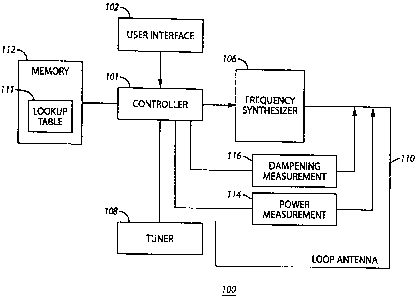
[0016] FIG. 1 comprises a block diagram of a universal transmitter
according to various
embodiments the present invention;
[0017] FIG. 2 comprises a circuit diagram of a universal transmitter
according to various
embodiments of the present invention;
[0018] FIG. 3 comprises a flowchart of one approach for transmitting
signals at multiple
frequencies according to various embodiments of the present invention; and
[0019] FIG. 4 comprises a lookup table utilizing for tuning an antenna
according to
various embodiments of the present invention.
[0020] Skilled artisans will appreciate that elements in the figures are
illustrated for
simplicity and clarity and have not necessarily been drawn to scale. For
example, the
dimensions and/or relative positioning of some of the elements in the figures
may be exaggerated
relative to other elements to help to improve understanding of various
embodiments of the
present invention. Also, common but well-understood elements that are useful
or necessary in a
commercially feasible embodiment are often not depicted in order to facilitate
a less obstructed
view of these various embodiments of the present invention. It will further be
appreciated that
certain actions and/or steps may be described or depicted in a particular
order of occurrence
while those skilled in the art will understand that such specificity with
respect to sequence is not
actually required. It will also be understood that the terms and expressions
used herein have the
ordinary meaning as is accorded to such terms and expressions with respect to
their
corresponding respective areas of inquiry and study except where specific
meanings have
otherwise been set forth herein.
- 4a -
CA 02646840 2008-12-17
Description
[0021] It will be appreciated that the approaches described herein are
particularly
useful and applicable to transmitters used in conjunction with moveable
barrier operator
systems. However, it will be appreciated that these approaches can be applied
to transmitters
that are used in other types of systems and are not limited to use with only
moveable barrier
operator systems.
[0022] Referring now to FIG. 1, one example of a universal transmitter that
utilizes
the present approaches is described. In this example, a transmitter 100
includes a controller
or processor 101 (coupled to a memory 112), a frequency synthesizer 106, a
single loop
antenna 110, and a tuner 108. A user interface 102 accepts input from a user
that indicates a
desired frequency to tune the single loop antenna 110. The controller 101
directs the
= operation of the tuner 108 and frequency synthesizer 106 to tune the
single loop antenna 110
to the appropriate desired frequency indicated by instructions received from
the user via the
user interface 102 and to transmit signals from the single loop antenna 110.
[0023] Various approaches can be used to tune the single loop antenna 110.
As
described below, a power measurement circuit 114, a dampening measurement
circuit 116,
and/or a lookup table 111 (stored in the memory 112) may be used to tune the
single loop
antenna 110. It will be understood that other elements, circuit components, or
data structures
may also be used to tune or assist in tuning the single loop antenna 110.
[0024] As mentioned, the synthesizer 106 forms signals to be transmitted at
the
desired operational center frequency via the antenna 110. In this regard, the
operational
center frequency is centered within a first band of frequencies and this first
band of
frequencies has a first bandwidth. To give one example, the first bandwidth
may be less than
approximately 5 MHz.
[0025] The single loop antenna 110 is structured to operate across a second
band of
frequencies that have a second bandwidth, and, in many of these approaches,
the first
bandwidth is less than the second bandwidth. In one example, the second
bandwidth of
ranges is from approximately 300 MHz to approximately 434 MHz.
- 5 -
CA 02646840 2008-12-17
[0026] The user interface 102 is any type of actuator or combination of
actuators that
is used to receive user input indicating a desired frequency to transmit
signals from the
transmitter 100. For example, the user interface 102 may be one or more
switches, dials,
levers, or buttons. In some examples, a separate actuator may be used to
indicate each
potential desired frequency and the corresponding actuator is actuated by a
user to transmit at
that frequency. In other examples, a single actuator is used for transmissions
at all
frequencies.
[0027] The single loop antenna 110 can also assume a number of forms and
structures. In some examples, the single loop antenna 110 is structured as a
printed circuit
board (PCB) antenna (e.g., a trace element). Other examples of antenna
structures or
configurations may also be used.
[0028] The tuner 108 tunes the single loop antenna 110 to the value of the
resonant
center frequency. The tuner 108 may include various electronic circuit
elements arranged in
a variety of different ways. In one example, the tuner 108 includes a
varactor. In some
approaches when a varactor is used, the voltage applied to the varactor
changes the value of
the resonant center frequency of the single loop antenna 110.
[0029] As mentioned, the memory 112 may include a lookup table 111 and this
may
be used by the controller 101 to apply signals to the tuner 108 and thereby
tune the single
loop antenna 110. In another example, the power of the transmitted signal is
measured by the
power measurement circuit 114, the controller 101 analyzes the received
information, and the
tuning is accomplished according to the measured power. In still another
example,
dampening of the transmitted signal is determined by the dampening measurement
circuit
116, the controller 101 analyzes the received information, and the single loop
antenna 110 is
tuned according to the dampening. Other examples of tuning arrangements and
procedures
are possible.
[0030] In one example of the operation of the system of FIG. 1, information
is
received at the user interface 102 indicating a value of a center frequency of
a signal to
transmit. The controller 101 analyzes the signal and operates the synthesizer
106 and tuner
108 to transmit information at the indicated center frequency.
[0031] The single loop antenna 110 is tuned by the tuner 108 to match a
desired value
of the center frequency. The signal is transmitted from the single loop
antenna 110
- 6
CA 02646840 2008-12-17
according to the value of the operational center frequency. The value of the
operational
center frequency may be changed to be another value and this other value, in
many of these
approaches, is within the second band of frequencies.
[0032] The signals sent from the single loop antenna 110 (and formed by the
synthesizer 106) themselves may include various types of information such as
codes that are
used to actuate a moveable barrier operator or some other device. For example,
these codes
may be fixed codes, rolling codes, or some combination of fixed and rolling
codes.
[0033] In many of these approaches, the Q-value provided by the single loop
antenna
110 is of an adequately high value. More specifically, the Q-value is of such
a value so as to
allow for the transmission of narrow band signals (e.g., 5 MHz) from the
single loop antenna
110 across a wide frequency range (e.g., 300-434 MHz). Moreover, these signals
are
transmitted with sufficient power so as to be easily detected by a moveable
barrier operator.
To take one example, the Q-value of the transmission circuit is greater than
approximately
10. Other examples of Q-values and other circuits providing differing Q-values
are possible.
Also, other circuit/antenna performance measurement factors can be used to
determine the
adequacy of the circuit so as to meet or exceed these criteria.
[0034] Referring now to FIG. 2, one example of a universal transmitter 200
is
described. The transmitter of FIG. 2 includes electronic components with
various values,
ranges, and tolerances. It will be appreciated that these values, ranges, and
tolerances are
examples only and other components connected in different arrangements and
having
different values, ranges, and tolerances may also be used to achieve the same
goals.
[0035] A synthesizer 202 receives a first signal 204 (also labeled as SO in
FIG. 2) and
a second signal 206 (also labeled as SCLK in FIG. 2) from a processor 201.
These signals
also drive a first switching circuit 208 and a second switching circuit 210.
In one example,
the synthesizer 202 may be a CC1152 device manufactured by Chipcon and the
processor
201 may be a 16F689 manufactured by Microchip Technology, Inc. Other examples
of
synthesizers and processors are possible. The first signal 204 (SO) and second
signal 206
(SCLK) are, respectively, low and high frequency clocked signals. The first
signal 204 (SO)
and the second signal 206 (SCLK) are digital serial communication busses and
conduct
communications at 100K baud.
- 7
CA 02646840 2008-12-17
[0036] The first switching circuit 208 and the second switching circuit
210 include
various electronic components. More specifically, the first switching circuit
208 includes a
first transistor 212 (also labeled as Q6 in FIG. 2), a first resistor 214
(e.g., a 10k ohm
resistor), and a second resistor 216 (e.g., a 47k ohm resistor). The second
switching circuit
210 includes a second transistor 218 (also labeled as Q7 is FIG. 2), a third
resistor 220 (e.g., a
10k ohm resistor), and a fourth resistor 222 (e.g., a 47k ohm resistor).
[0037] A first capacitor 224 (C30, e.g., 1 micro farad) and first inductor
226 (L6, e.g.,
470 micro henries) receive a voltage from the power supply Vdd (e.g., 3 volts)
and operate to
create a fly back voltage at a point 228 that is higher than Vdd. The
generated voltage at
point 228 is applied to diodes 230 (also labeled as D12 in FIG. 2) and is fed
back (via the
feedback line 235 also labeled as BST_FDBCK) to the processor 201 via resistor
network
232. The resistor network 232 includes a resistor 234 (also labeled as R11 in
FIG. 2, e.g.,
49.9k ohms) and a resistor 236 (also labeled as R2 in FIG. 2, e.g., 402k
ohms). The voltage
also has noise removed by a second capacitor 238 (also labeled as C27 in FIG.
2, e.g., 4.7
microfarads) and a third capacitor 240 (also labeled as C7 in FIG. 2, e.g., 22
pico farads) and
the voltage is limited by a voltage limiting diode 242 (also labeled as D13 in
FIG. 2). A fifth
resistor 244 (also labeled as R10 in FIG. 2, e.g., 100k ohms) limits the
current to the varactor
246 (also labeled as DIO in FIG. 2).
[0038] The synthesizer 202 is coupled to a matching network 248 that
matches the
impedance of an antenna 250 with the impedance at the output of the
synthesizer 202. The
matching network 248 includes a fourth capacitor 252 (also labeled as C25 in
FIG. 2, e.g., .01
micro farads), a fifth capacitor 254 (also labeled as C16 in FIG. 2, e.g., 6.8
micro farads), a
sixth capacitor 256 (also labeled as C17 in FIG. 2, e.g., 220 pico farads),
and a seventh
capacitor 258 (also labeled as C21 in FIG. 2, e.g., 6.8 pico farads). The
matching network
248 also includes a second inductor 260 (also labeled as L7 in FIG. 2, e.g.,
33 nano henries).
The synthesizer 202 produces a modulated signal for transmission by the
antenna 250. The
signal may include various type of information, for example, various types of
codes.
[0039] A harmonic filter 262 removes undesirable harmonics from the signal
produced by the synthesizer 202. For instance, various lower range harmonics
(e.g., the
second and third harmonics) may be removed by the harmonic filter 262. In this
example, the
harmonic filter 262 includes a third inductor 264 (also labeled as L4 in FIG.
2, e.g., 18 nano
- 8 -
i
CA 02646840 2008-12-17
henries), and a fourth inductor 266 (also labeled as L5 in FIG. 2, e.g., 33
nano henries). The
harmonic filter 262 also includes an eighth capacitor 268 (also labeled as C12
in FIG. 2, e.g.,
pico farads), a ninth capacitor 270 (also labeled as C6 in FIG. 2, e.g., 6.8
pico farads), a
tenth capacitor 272 (also labeled as C 18 in FIG. 2, e.g., 220 pico farads),
an eleventh
capacitor 274 (also labeled as C13 in FIG. 2, e.g., 33 pico farads), and a
twelfth capacitor 276
(also labeled as C14 in FIG. 2, e.g., 15 pico farads).
[0040] The antenna 250 is coupled between the harmonic filter 262 and the
varactor
246. The antenna 250 is a single loop antenna and, in one approach, is a trace
element on a
printed circuit board (PCB). Other elements or approaches may also be used to
construct the
antenna 250.
[0041] The synthesizer 202 receives information via a signal line 278
(labeled as SI in
FIG. 2). Signal line 278 transmits information from the processor 201
indicating a desired
frequency that the user wishes to tune the antenna 250. This information may
itself be
received by the processor 201 from one or more buttons, switches, or other
types of actuators.
Once the synthesizer 202 receives the information, it is processed and
transmits first and
second signals 204 and 206 to drive the circuits 208 and 210. This, in turn,
increases the
voltage in the inductor 226 (L6) and these signals are applied until voltage
value on the
feedback line 235 indicates to the processor 201 that the voltage at the
varactor 246 has
reached the needed level in order to tune the antenna 250 to the desired
frequency. When the
desired frequency is reached, the processor 201 halts transmission of the
first and second
signals 204 and 206. In this same manner, the processor 201 may resume
application of the
first and second signals 204 and 206 as the voltage across the varactor 246
drops in order to
maintain the voltage across the varactor 246 at the desired level and maintain
the tuning of
the antenna 250.
[0042] The circuit of FIG. 2 also has other components configured to
provide for
proper operation of the synthesizer 202. These include a thirteenth capacitor
278 (also
labeled as C22 in FIG. 2, e.g., 0.1 micro farads), fourteenth capacitor 280
(also labeled as
C11 in FIG. 2, e.g., 220 micro farads), fifteenth capacitor 282 (also labeled
as C 10 in FIG. 2,
e.g., 0.1 micro farads), sixteenth capacitor 284 (also labeled as C24 in FIG.
2, e.g., 220 pico
farads), seventeenth capacitor 286 (also labeled as C23 in FIG. 2, e.g., 220
pico farads),
eighteenth capacitor 288 (also labeled as C28 in FIG. 2, e.g., 0.01 micro
farads), nineteenth
- 9
CA 02646840 2013-12-17
=
capacitor 290 (also labeled as C8 in FIG. 2, e.g., 27 pico farads), twentieth
capacitor 292 (also
labeled as C9 in FIG. 2, e.g., 27 pico farads), resistor 294 (also labeled as
R12 in FIG. 2, e.g.,
56k ohms), and oscillator 296. It will be understood that these components are
provided here
and connected as shown since the synthesizer 202 is a CC1152 device in this
example. If other
synthesizers are used, the supporting components, values of components, and
connections used
are likely to differ.
[0043] In one example of the operation of the circuit of FIG. 2, a user
the changes the
resonant center frequency of the antenna 250 via application of a control
voltage to the varactor 246.
More specifically, user input is received from a user interface at the
processor 201. The processor
201 analyzes the signal and determines the desired resonant center frequency.
The processor 201
then activates the signals 204 and 206 to drive the forward voltage across the
varactor 246 to the
level needed to produce the desired resonant center frequency at the antenna
250. The synthesizer
202 modulates a signal and applies the signal to the antenna 250 and the
antenna 250 transmits the
signal at the desired center frequency.
[0044] As mentioned, the antenna 250 is terminated by the varactor 246.
The capacitance
of the varactor 246 is controlled by a voltage across the varactor 246. In one
example, the voltage
applied to the varactor 246 can change from Vdd (in this example, 3 volts) to
18 volts. For instance,
when the boost voltage across the varactor 246 is set to 3 volts, the resonant
center frequency of the
antenna 250 is set to be 300 MHz. On the other hand, when the boost voltage is
set to 18 volts, the
resonant center frequency of the antenna 250 is set to 434 MHz. The
capacitance of the varactor 246
decreases and the resonant frequency increases as the forward voltage across
the varactor 246
increases. The type and ratings of the varactor 246 are adjusted to control
the minimum capacitance
and, correspondingly, the maximum frequency that can be achieved by the
antenna 250.
[0045] Referring now to FIG. 3, one example of an approach for
generating multiple signals
having different frequencies at a transmitter is described. At step 302, user
instructions are received.
These may be received at a user interface, for example, from actuators (e.g.,
switches, dials, levers,
buttons, or the like) to indicate the desired frequency. In one example, a
single actuator (e.g.,
button) is used for all frequencies. In another example, a different actuator
(e.g., button) is used for
each frequency.
- 10-
CA 02646840 2008-12-17
[00461 At step 304 a value of a center frequency of a signal to transmit
is determined
according to received user input. The center frequency is centered within a
first band of
frequencies and the first band of frequencies has a first bandwidth.
[0047] At step 306, a single loop antenna is tuned to match the first
value of the
center frequency. This single loop antenna is arranged and configured to
operate across a
second band of frequencies having a second bandwidth and, in this example, the
first
bandwidth is less than the second bandwidth.
[0048] The tuning can be accomplished utilizing a variety of different
approaches. In
one example, the tuning is accomplished using a lookup table. In another
example, the power
of the transmitted signal is measured and the tuning is accomplished according
to the power.
In still another example, dampening of the transmitted signal is determined
and the antenna is
tuned according to the dampening. Other examples of tuning approaches are
possible.
[0049] At step 308, the signal is transmitted from the single loop antenna
according to
the first value of the operational center frequency to provide a transmitted
signal. Subsequent
to step 308, the first value of the center frequency may be changed to be a
second value and
this second value is also within the second band of frequencies. To take one
specific
example, transmissions are made in the 300-434 MHz range and the frequency of
the
transmitted signals can be adjusted from 300 to 310 MHz.
[0050] Referring now to FIG. 4, one example of a lookup table 400 used in a
universal transmitter according to the present approaches is described. The
table 400
includes a series of rows 402 and columns 404.
[0051] Each row 402 may include an indictor value 406, desired frequency
value 408,
and an associated voltage value 410. The indicator value 406 is a data
representation of a
particular actuation of an actuator (e.g., the pressing of a particular button
or the pressing of a
button in a certain way). The voltage value 410 is the voltage desired to be
applied to the
varactor. Once the voltage value 410 is determined, the controller or
processor transmits
appropriate signals to a tuning circuit and/or synthesizer to adjust the value
of the voltage
across the varactor that produces the desired resonant center frequency for
transmissions.
Once the voltage is adjusted, the antenna is tuned to transmit at the
appropriate frequency.
-11-
CA 02646840 2008-12-17
100521 To take one example, if the user desires to transmit at 340 MHz, an
actuator is
actuated forming an indicator 15 associated with the desired frequency of 340
MHz. The
table 400 is examined to find the indicator 15, and, in this example, an
indicator 15 is found in
row 412 that has a particular voltage value (in this case 9.7 volts). The
processor or
controller is operated so as to cause the voltage across the varactor to be
9.7 volts. This
action causes the antenna to be tuned to have a resonant center frequency of
approximately
340 MHz.
[0053] It will be appreciated that the lookup table of FIG. 4 is only one
example of a
data structure and that other examples of lookup tables having other types of
information or
other types of data structures are possible. It will also be appreciated that
other circuit
elements may be utilized instead of the varactor to tune the antenna to the
frequency desired
by the user.
[0054] Thus, universal transmitters are provided for use in conjunction
with moveable
barrier operator systems. The approaches provided herein utilize a single,
tuned circuit that
provides adequate Q-values so that transmissions can be made across an entire
frequency
spectrum at adequate power, for example, across the 300-434 MHz spectrum.
Additionally,
the transmitters that utilize these approaches are small, light weight,
portable and can be
powered by a conventional battery.
[0055] Those skilled in the art will recognize that a wide variety of
modifications,
alterations, and combinations can be made with respect to the above described
embodiments
without departing from the spirit and scope of the invention, and that such
modifications,
alterations, and combinations are to be viewed as being within the scope of
the invention.
- 12 -