Note: Descriptions are shown in the official language in which they were submitted.
CA 02647388 2008-09-25
1
A switching device
The invention relates to a switching device such as a residual-current breaker
or a combination
switch for example, for interrupting and switching at least one line,
comprising a tripping device
which is independent of the system voltage, a tripping element associated with
said tripping
device such as a tripping relay for example, and a tripping device which is
dependent on the
system voltage.
Such switching devices are used in electrical engineering, especially in
building installations
such as household installations. When an undesirable state occurs such as a
residual current,
excess current or excess voltage, such switching devices are intended to
respond and cut the
affected circuit from voltage supply.
Residual-current devices (RCDs) or combination switches (RCBOs) are classified
according to
their technical functions as independent of system voltage ("VI" or voltage
independent) or as
dependent of system voltage ("VD" or voltage dependent). Full functional
capability is also
given in the case of failed system voltage (VI) in the first case according to
relevant product
standards (e.g. EN/IEC 61008, 61009, 61947...). In the latter case however,
this is only the case
in the presence of the supplying system voltage (VD).
A residual-current circuit breaker was already published in the international
publication WO
2006/007 608 A2, which in addition to its voltage-independent basic function
can receive an
optionally installable additional module (open-loop and closed-loop control
module) which
enables voltage-dependent additional functions. Two tripping elements are
provided for this
purpose in the residual-current breaker, whereof the one acts in a voltage-
independent way
(permanent-magnet trip element) on a common breaker mechanism and the other in
a voltage-
dependent way (open-circuit shunt release). When the additional module is
inserted and a supply
voltage is applied, the voltage-independent trip element is bridged and only
the voltage-
dependent trip element is triggered.
CA 02647388 2008-09-25
2
The disadvantageous aspect in this switching device is the high constructional
complexity, since
many modules need to be present twice for voltage-independent and voltage-
dependent tripping.
Since a separate trip element needs to be provided for both types of tripping,
this applies
especially to implementations in which the subsequent installation of an
additional module is not
provided.
DE 198 42 470 A 1 describes a residual-current current breaker with overload
protection, with a
residual-current tripping circuit which is independent of system voltage and
an overload tripping
circuit which is dependent of system voltage that act on the same tripping
relay.
EP 570 603 Al discloses a fail-safe differential-current circuit breaker, with
the same comprising
evaluation electronics which are dependent of system voltage and which is
associated with a first
tripping relay which upon loss of the supply voltage of the evaluation
electronics would trip the
breaker mechanism. In order to avoid this, the circuit breaker further
comprises a second tripping
relay which also acts upon the breaker mechanism and which would also trigger
the breaker
mechanism upon loss of the supply voltage. In order to prevent this, the
breaker mechanism is
arranged in such a way that the same will only trip when it is triggered by
one of the two tripping
relays.
A residual-current circuit breaker which is independent of system voltage is
disclosed by WO
2006/007608 A which is extended by further functionalities by inserting an
additional module
which is dependent of system voltage.
It is therefore the object of the present invention to further develop a
switching device of the kind
mentioned above in such a way that the same can further be operated with and
without an
additional module, but has a simpler arrangement in this connection. In
particular, no modules
need to be necessary which are not required for mere voltage-independent
operation in the case
of operation of the switching device without an additional module, i.e. when
therefore merely the
voltage-independent basic functions are provided. Moreover, conventional
voltage-independent
switching devices shall be easily adjustable and the functional reliability in
voltage-dependent
operation is to be increased.
This object is achieved in accordance with the invention in such a way that
the tripping device
which is dependent on the system voltage comprises means for tripping the
tripping element
which is associated with the tripping device which is independent of the
system voltage. The
CA 02647388 2008-09-25
2a
tripping device which is dependent of the system voltage therefore uses the
tripping device
which is independent of the system voltage which is present anyway.
It is thus possible to use the switching element optionally with or without
the additional module.
A further tripping element can thus be avoided even when using the additional
module and using
the voltage-dependent extended functions.
According to an advantageous embodiment, a summation current transformer with
at least one
primary winding for detecting a critical current and with a secondary winding
for supplying a
tripping current to the tripping device which is independent of the system
voltage can be
provided. Residual currents can thus be recognized and the tripping
functionality which is
independent of system voltage which is mostly required can thus be ensured.
It can be provided in this connection that the summation current transformer
comprises an
additional tertiary winding. Unintended tripping can be avoided, especially in
the case of
transient overvoltage and its follow currents.
The tripping device which is dependent of the system voltage can be arranged
in this context for
supplying an electric current to the tertiary winding. By supplying a current
to the tertiary
winding it is possible to realize a tripping control since an increased
magnetic current linkage
occurs in the summation current transformer. It then activates the tripping
element of the tripping
device which is independent of the system voltage, e.g. a permanent magnet
relay. In this way,
the tripping device which is dependent of the system voltage....
CA 02647388 2008-09-25
3
possible to realize a tripping control since an increased magnetic current
linkage occurs in the
summation current transformer. It then activates the tripping element of the
tripping device
which is independent of the system voltage, e.g. a permanent magnet relay. In
this way, the
tripping device which is dependent of the system voltage can trip the tripping
device which is
associated with the tripping device which is independent of the system
voltage, e.g. the
permanent magnet relay.
According to a further embodiment of the invention, the tripping device which
is dependent
of the system voltage can be switched between secondary winding and tripping
element. In
this case, a passive electronic tripping system which is switched between the
summation
current transformer and tripping relay can be especially provided and may be
optionally
combined with the tripping device which is dependent of the system voltage
into an assembly,
especially in a module.
In this connection it can be provided that the tripping device which is
dependent of the
system voltage is arranged for supplying an electric current to the tripping
element. This has
the advantage that the tripping device which is dependent of the system
voltage can cause a
direct tripping of the tripping element associated with the tripping device
which is
independent of the system voltage.
In a preferred embodiment, the tripping device which is dependent of the
system voltage can
be arranged in the form of a module combined into a functional group. It is
thus easily
possible in an especially simple manner to create various embodiments with or
without
functions which are dependent on system voltage. According to one variant, the
module can
be arranged in a fixed manner in the switching device. It would alternatively
be possible
according to another variant to arrange the module in a removable way,
preferably via plug-in
contacts, in the switching device. In the latter embodiment, functions which
are dependent of
system voltage can be retrofitted subsequently.
Advantageously, the tripping device which is dependent of the system voltage
can be
activated in the at least one line in the case of application of a supply
voltage. This leads to
the advantage that a change from voltage-dependent to voltage-independent
operation or
vice-versa can occur automatically.
CA 02647388 2008-09-25
4
It can preferably be provided that the tripping device which is dependent of
the system
voltage is activated in the at least one line upon exceeding a predeterminable
threshold value
of the voltage. Switching to the voltage-dependent operation is only made when
full
functional capability of the tripping device which is dependent of the system
voltage is
guaranteed. The predeterminable threshold value can be between 30 and IOOV,
preferably
between 50 and 80V. It is thus ensured that upon application of a contact
voltage which is
dangerous for humans the high security of the tripping device which is
dependent of the
system voltage is already available.
Preferably, the tripping device which is dependent of the system voltage can
be deactivated
upon falling below the predeterminable threshold value of the voltage in the
at least one line.
The switching device acts like a circuit which is purely independent of system
voltage, so
that a secure function of the switching device is ensured at all times.
A time-delay circuit, which is preferably independent of system voltage, can
be provided in a
further embodiment of the invention, which circuit renders ineffective the
tripping device
which is dependent of the system voltage during a predeterminable time
interval after its
activation, preferably during I to 100 msecs. The time can thus especially be
bridged which
the tripping device which is dependent of the system voltage requires during
activation until
its full functional capability has been reached. False tripping which may be
caused by a
tripping device which is dependent of the system voltage and has not yet
reached full
functional capability can thus reliably be avoided in this time interval.
In this connection it can be provided that the time-delay circuit bridges the
tripping device
which is dependent of the system voltage during the predeterminable time
interval. The
tripping device which is dependent of the system voltage can thus be rendered
ineffective in
an especially simple way.
The invention is now explained in closer detail by reference to the enclosed
drawings
showing embodiments in an exemplary way, wherein:
Fig. I shows a residual-current circuit breaker with a tertiary winding
according to the known
state of the art;
CA 02647388 2008-09-25
Fig. 2 shows a first embodiment of a residual-current circuit breaker in
accordance with the
invention;
Fig. 3 shows a residual-current circuit breaker with a power-amplifying
passive circuitry
according to the known state of the art;
Fig. 4 shows a second embodiment of a residual-current circuit breaker
according to the
invention;
Fig. 5a shows a detail of an additional module with an integrated electronic
system which is
independent of system voltage according to a first embodiment of the
invention;
Fig. 5b shows a detail of an additional module with integrated electronic
system which is
independent of system voltage in accordance with the second embodiment of the
invention;
Fig. 5c shows a detail of an additional module with a separate electronic
system which is
independent of system voltage in accordance with the first embodiment of the
invention;
Fig. 5d shows a detail of an additional module with a separate electronic
system which is
independent of system voltage in accordance with the second embodiment of the
invention.
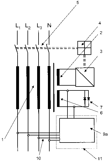
Fig. I shows a known residual-current circuit breaker with four lines, which
are the outer
conductors LI, L2, L3 and the neutral conductor N, a summation current
transformer 1, a
secondary winding 2, a tertiary winding 6 and a tripping element which is
arranged as a
permanent-magnet tripping relay 3. The tripping relay 3 is in connection with
a breaker
mechanism 4 which acts on its part on the main contacts 5. During the
occurrence of a
residual current in one of the conductors Li, L2, L3 or N, a voltage is
induced in the secondary
winding 2, through which the permanent-magnet tripping relay 3, which is
connected to the
same, responds and thus leads to the tripping of the circuit breaker and thus
to a severing of
the main contacts 5 via the breaker mechanism 4.
Switching elements which are independent of voltage such as this residual-
current circuit
breaker obtain their tripping energy via the summation current transformer 1
directly from the
energy of the residual current. Due to the high sensitivity of such tripping
circuits, there is
always the possibility of undesired tripping, e.g. during the occurrence of
transient
overvoltage and its follow current. These undesirable phenomena are
counteracted for
example through special additional windings such as the tertiary winding 6 of
the summation
current transfonner 1 as shown in Fig. 1, which tertiary winding transmits
magnetic field
energy from the summation current transformer I into said additional winding 6
at high
residual-current amplitudes via two diodes 7 which are switched in an
antiparallel way.
CA 02647388 2008-09-25
6
Energy transfer to the tripping element coupled on the secondary side is
reduced, which in the
illustrated case is the permanent-magnet tripping relay 3, so that the same
does not respond.
In the first embodiment in accordance with the invention as shown in Fig. 2,
said tertiary
winding 6 is used for linking an additional module 9a to the tripping which is
dependent on
system voltage. This principle of controlled magnetic flux in the summation
current
transformer 1 is used in the present invention in order to realize the
tripping control for the
application case which is independent or dependent on system voltage by high-
resistance or
low-resistance termination of the tertiary winding 6. In this respect, only a
single tripping
relay is necessary, namely the permanent-magnet tripping relay 3. In operation
which is
independent of voltage (VI), the module input at module 9a is of high
resistance, so that the
module 9a does not influence the VI tripping circuits. In the presence of a
minimum voltage
at module 9a, the above input becomes low-resistant. Any present differential
current induces
a current in the tertiary winding 6 which is prepared in module 9a (analog-to-
digital converter)
and is detected. Upon exceeding a preconfigurable threshold value, a test
current is generated
in module 9a and supplied to tertiary winding 6. Due to the high number of
turns of the
tertiary winding (e.g. between 20 and 200, preferably 50 to 120, especially
80), an increased
magnetic current linkage is induced in the summation current transformer I by
these
increased ampere-turns, which increased magnetic current linkage activates the
permanent-
magnet relay 3 in the secondary circuit via the secondary winding 2. As
compared with use
which is independent of system voltage, the triggering of the permanent-magnet
relay 3
occurs with increased energy, which in the border case occurs until saturation
of the
summation current transformer material has occurred, thus enabling an
improvement in the
tripping reliability of the relay 3.
By feeding the test voltage to the tertiary winding 6, the permanent-magnet
relay 3 can be
triggered by a tripping device 9 which is dependent of the system voltage and
a tripping of
the residual-current circuit breaker can thus be caused without requiring a
separate tripping
element which is dependent of the system voltage.
In addition to the residual-current circuit breaker as shown in Fig. 1, prior
known tripping
circuits like the one shown in Fig. 3 are in use. Passive electronic tripping
system 8 is
switched between the summation current transfonner I and the tripping relay 3
in order to
achieve reliable tripping or to maintain a purposeful delay of the same. The
latter applies for
CA 02647388 2008-09-25
7
example for the characteristics "S" as defined in the standard. A permanent-
magnet tripping
relay 3 which can actuate the breaker mechanism 4 is also used here as a
tripping element
which is independent of the system voltage.
It is also provided here in accordance with the invention to arrange a
tripping device which is
dependent of the system voltage and to arrange the same in such a way that it
can trip the
tripping element, which is the permanent-magnet relay 3 and is associated with
the tripping
device which is independent of system voltage. Since no tertiary winding is
present under
certain circumstances, it is provided according to a second embodiment of the
invention to
realize the linkage of the system-voltage-independent functions via a module
part 9b which
can integrate the passive electronic tripping system 8 (see Fig. 4). Module 9b
can act directly
on the permanent-magnet relay 3 and cause a tripping of the residual-current
circuit breaker
through the same.
It can be provided that the additional functions which are dependent on system
voltage are
combined in an additional module 11 which can be optionally arranged or is
removable again.
Without this additional module 11, the circuit breaker then acts like a
conventional switch
which is arranged in a purely voltage-independent way. When the additional
module 11 is
inserted into the same, it is supplemented by system-voltage-dependent
additional functions
of the module 9a (Fig. 2) or 9b (Fig. 4). In order to secure the voltage-
independent function
even when additional module 11 has been inserted, the VI electronic tripping
system which is
independent of system voltage can be functionally integrated in this module 11
according to
an advantageous embodiment (also see Fig. 5b for example, detail 8b), so that
in this case the
module 11 can contain both system-voltage-independent (VI) as well as system-
voltage-
dependent (VD) functionalities.
The two functional groups for system-voltage-dependent (VD) and system-voltage-
independent (VI) tripping can be arranged in two module parts in a spatially
separated way.
The system-voltage-independent (VI) are combined in a module part 9a-1 or 9b-1
and the
system-voltage-dependent (VD) functions in a module part 9a-2 or 9b-2.
The system-voltage-dependent tripping function of the embodiment as shown in
Fig. 4 will
be explained below: The residual-current signal generated by the summation
current
transformer I is prepared and detected by the electronic system 9b in module
11. Upon
CA 02647388 2008-09-25
8
exceeding a preconfigurable threshold value, a test current is generated in
module 11 and
output to the tripping relay 3. Said signal occurring at the output of module
I 1 is more
powerful than the tripping signal provided in VI operation by the electronic
tripping system
8b or 8d. This leads to an increase in the tripping reliability of the
inductively coupled
tripping relay 3 in VD operation.
The value of the minimum supply voltage for activating the VD functions in
such a hybrid
module ("VIVD") lies in the range of 30 to 100 V, preferably between 50 and 80
V.
In addition, further functions can be integrated in the switching device or in
the module 11.
For example, an intetnal temperature detection can enable the detection of
excess temperature
which can be further processed concerning the evaluation of the thermal
reliability of the
used electronic components in module 11. The device can be switched off under
thermal
overload for example. In particular, different protective requirements can be
fulfilled by
exchanging different types of modules while the voltage-independent basic
function is
provided by the same base switch.
The common aspect of all module types is the possibility of realizing
additional functions in
the VD mode:
- Adjustability of a threshold value of the residual operating current (e.g.
ID between
0.5 IDn and approx. 0.95 IDn)
- Adjustability of a tripping delay
- Adjustability of a high and/or low voltage limit for detecting overvoltage
and/or
undervoltage
- Determination of the power factor of the residual current
- Communication channel to the outside via infrared, visible LEDs, radio,
.....
- Data interface for exchanging program code, parameters, ......
In a further development of the invention, the functional reliability of the
switching device
can be improved even further. Since a finite amount of time is required from
switching on the
switching device until the provision of the full scope of functions of module
11, even if this is
only in the range of milliseconds, it is possible that the occurrence of
transient impulse
currents can lead to an unintentional tripping of the residual-current circuit
breaker. Such
CA 02647388 2008-09-25
9
transient impulse currents can occur by the activation of inductive loads for
example. It is
therefore desirable to prevent such justified undesirable tripping during this
time interval. It
can therefore be provided in a switching device in accordance with the
invention that the
functionality of the module 11 is bridged by a time-delay circuit until the
module 11 is able to
prevent such undesirable tripping according to its configuration. Such a time-
delay circuit
which is independent of system voltage can either be integrated in module 11
(see Fig. 5a and
5b) or be realized as a separate circuit (see Fig. 5c and 5d) which is
connected with the
module 11.
Bridging can be realized in the following manner for example: In the
embodiment according
to Figs. 4 and 5b, the input of module part 9b is high-resistant in system-
voltage-independent
VI operation, so that the function of electronic system 8 is active. Upon
exceeding a threshold
value of the supply voltage, the system-voltage-independent VI function
changes to the
system-voltage-dependent VD function. The input of the module part 9b which is
dependent
of system voltage becomes low-resistant and the electronic tripping system 9b
is bridged.
An arrangement of bridging in the example according to Figs. 2 and 5a is
respectively
possible.
When a tripping circuit is provided which requires a power-amplifying passive
circuitry (as
shown in Fig. 3 with detail 8), it can also be combined with the additional
time-delay circuit
(see Figs. 5b and 5d, details 8b and 8d).
Further embodiments in accordance with the invention merely have a part of the
described
features, with any combination of features being provided, especially also of
different
described embodiments.