Note: Descriptions are shown in the official language in which they were submitted.
CA 02648410 2008-12-30
1
CLOCK GENERATION CIRCUIT, ANALOG-DIGITAL ANGLE
CONVERTER USING THE SAME, AND ANGLE DETECTION
APPARATUS
BACKGROUND OF THE INVENTION
FIELD OF THE INVENTION
[0001] The present invention relates to a clock generation circuit for
generating a synchronous clock from two-phase resolver signals, an
analog-digital angle converter having the clock generation circuit, and an
angle detection apparatus.
DESCRIPTION OF THE RELATED ART
[0002] Fig. 12 shows a clock generation circuit used in a conventional
angle converter disclosed in Japanese Patent No. 3,100,211 (Japanese Patent
Application Laid-Open No. H5-172505).
[0003] A resolver signal Kl = KsinOsinwt and a resolver signal K2 =
Kcos0sincot obtained, for example, in a resolver 1 A are input to an
analog-digital converter (hereinafter called an A-D converter) 2. The
resolver signals Kl and K2 are also input to a pair of squaring circuits 3a
and 3b, respectively. The squaring circuits 3a and 3b square the resolver
signals K1 and K2 to output squared signals Y1 = K2sin20sin2cot and Y2 =
K2cos20sin2wt. An adding circuit 4 adds the squared signals Y1 and Y2 to
output a sum signal 4a = K2sin2wt because sin20 + cos20 = 1. A square-root
circuit 5 square-roots the sum signal 4a to output a signal R = Ksinwt. A
level adjustment circuit 6 adjusts the amplitude of the signal R to output a
CA 02648410 2008-12-30
2
signal K'sincot. This signal K'sinwt is input to a REF terminal 2c of the
A-D converter 2. The A-D converter 2 uses the signal K'sinot as a
synchronous clock and outputs a digital angle signal 2d from the angle
signals K 1 and K2.
[0004] As described above, the conventional clock generation circuit
requires the square-root circuit in order to obtain the synchronous clock.
Since the square-root circuit uses an analog multiplier, it is relatively
expensive.
SUMMARY OF THE INVENTION
[0005] In view of the foregoing situation, the present invention has been
made. An object of the present invention is to provide a clock generation
circuit for generating a synchronous clock without using a square-root
circuit, an analog-digital angle converter provided with the clock generation
circuit, and an angle detection apparatus.
[0006] A clock generation circuit according to the present invention
generates a synchronous clock from two-phase resolver signals S 1 and S2
corresponding to a rotation angle, the two-phase resolver signals being
output from a rotation angle detector when an excitation signal is supplied.
The clock generation circuit includes a first squaring circuit for squaring
the
resolver signal S 1; a second squaring circuit for squaring the resolver
signal
S2; an adding circuit for adding output signals from the first and second
squaring circuits; a rectangular-wave generator for generating a
rectangular-wave signal from an output signal from the adding circuit; a
phase shifter for correcting a phase of the rectangular-wave signal from the
CA 02648410 2008-12-30
3
rectangular-wave generator; and a frequency dividing circuit for dividing by
2 an output signal from the phase shifter in frequency in synchronization
with the excitation signal.
[0007] An analog-digital angle converter according to the present
invention includes the above-described clock generation circuit and a
calculation processing section adapted to output a digital angle of the
rotation angle by using the resolver signals S 1 and S2 and the synchronous
clock generated by the clock generation circuit.
[0008] An angle detection apparatus according to the present invention
includes a rotation angle detector that has windings for detection and
windings for excitation and that is adapted to output two-phase resolver
signals corresponding to a rotation angle through the windings for detection
when an excitation signal is supplied to the windings for excitation, and the
above-described analog-digital angle converter.
EFFECTS OF THE INVENTION
[0009] According to the present invention, a clock generation circuit can
be provided without using a square-root circuit required by a conventional
clock generation circuit.
BRIEF DESCRIPTION OF THE DRAWINGS
[0010] Fig. 1 is a block diagram showing the functional structure of a
clock generation circuit according to an embodiment of the present
invention;
Fig. 2A is a graph showing resolver signals S 1 and S2;
CA 02648410 2008-12-30
4
Fig. 2B is a graph showing the output signal waveforms from first
and second squaring circuits;
Fig. 2C is a graph showing the output signal waveform from an
adding circuit;
Fig. 2D is a graph showing the output signal waveform from a filter;
Fig. 3 is a graph used to describe a phase shift between the output
signal from the adding circuit and the output signal from a comparator:
Fig. 4A is a graph showing the output signal waveform from the
comparator;
Fig. 4B is a graph showing the output signal waveform from a phase
shifter;
Fig. 4C is a graph showing the output signal waveform from a
frequency dividing circuit;
Fig. 5 is a block diagram showing an example structure of the phase
shifter;
Fig. 6 is a block diagram showing an example structure of the
frequency dividing circuit;
Fig. 7A is a timing chart showing the operation of the frequency
dividing circuit when angle signals S 1 and S2 are delayed in phase from an
excitation signal;
Fig. 7B is a timing chart showing the operation of the frequency
dividing circuit when the angle signals S 1 and S2 have a phase lead with
respect to the excitation signal;
Fig. 7C is a timing chart showing the operation of the frequency
dividing circuit when a rectangular-wave excitation signal is given a phase
CA 02648410 2008-12-30
lead of 90 degrees;
Fig. 8 is a block diagram showing the functional structure of an
analog-digital angle converter according to an embodiment of the present
invention;
5 Fig. 9 is a block diagram showing an example structure in which the
frequency dividing circuit is formed of a comparator, a+90 phase shifter,
and a DFF;
Fig. 10 is a block diagram showing a part of a clock generation
circuit where a low-pass filter is used;
Fig. 11 is a block diagram of an angle detection apparatus according
to an embodiment of the present invention; and
Fig. 12 is a block diagram of a conventional clock generation circuit.
DETAILED DESCRIPTION OF THE PREFERRED EMBODIMENTS
[0011] Embodiments of the present invention will be described below by
referring to the drawings. Identical symbols are assigned to identical
components in multiple figures, and a description of the components is not
repeated.
[Clock generation circuit]
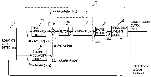
[0012] Fig. 1 shows the functional structure of a clock generation circuit
100 according to an embodiment of the present invention. The clock
generation circuit 100 includes first and second squaring circuits 11 and 12,
an adding circuit 14, a rectangular-wave generator 15, a phase shifter 20, and
a frequency dividing circuit 22.
[0013] Two-phase resolver signals output from a rotation angle detector 10
CA 02648410 2008-12-30
6
are input to the clock generation circuit 100. The rotation angle detector 10,
for example, a resolver, outputs two-phase resolver signals based on a
rotation angle. The resolver includes a rotor and a stator. One of the rotor
and the stator is wound with single-phase windings for excitation and the
other is wound with two-phase windings for detection. When a periodic
excitation signal E = Asincot is supplied to the windings for excitation,
two-phase periodic resolver signals S 1 and S2 based on the rotation angle 0
of the rotor with respect to the stator are obtained. Specifically, the
resolver signal S 1= AcosOsin(cot +~) is output through a first-phase
winding for detection and the resolver signal S2 = Asin0sin(wt +~) is output
through a second-phase winding for detection. The resolver signals are
hereinafter called angle signals. In the foregoing expressions, A indicates a
constant, t indicates time, co indicates the angular velocity, and ~ indicates
the phase difference between the phase of the excitation signal E and the
phase of the angle signals. The phase difference ~ occurs because the
rotation angle detector 10 uses electromagnetic coupling between the
windings for detection and the windings for excitation. The phase of the
angle signals is usually delayed from the phase of the excitation signal E by
several degrees below 20 degrees. The angle signals S 1 and S2 have
amplitudes corresponding to the rotation angle 0, have the same phase, and
are delayed in phase from the excitation signal E.
[0014] The angle signals S 1 and S2 are input to the first squaring circuit 11
and the second squaring circuit 12, respectively. The first squaring circuit
11 squares the amplitude of the angle signal S 1 to output a squared angle
signal S l a= A2cos20sin2((Ot +~). The second squaring circuit 12 squares
CA 02648410 2008-12-30
7
the amplitude of the angle signal S2 to output a squared angle signal S2a =
A2sin20sin2((ot + ~). Since sin2((ot + ~) = (1 - cos2(wt + ~))/2, the
frequency of the squared angle signals S 1 a and S2a is twice that of the
angle
signals S 1 and S2.
[0015] The adding circuit 14 adds the squared angle signals S 1 a and S2a to
output a sum signal a= A2sin2((Ot +~) because sin20 + cos20 = 1 in the sum
A2(sin26 + cos20)sin2((Ot + 0).
[0016] The rectangular-wave generator 15 generates a rectangular-wave
signal from the sum signal a. The rectangular-wave generator 15 includes
a filter 16 and a comparator 18. The filter 16 removes a DC component
from the sum signal a to output a signal [i. The comparator 18 compares
the signal 0 output from the filter 16 with a reference potential to output a
rectangular-wave signal SQ1. The reference potential is a ground potential
of an analog circuit comprising the filter 16 and the comparator 18 in the
present embodiment.
[0017] Since the comparator 18 converts the signal 0 to the
rectangular-wave signal SQ1 with the ground potential being used as a
reference, a phase shift occurs. In other words, the rectangular-wave signal
SQ 1 is shifted in phase from the sum signal a. The phase shifter 20
corrects this phase shift to output a corrected rectangular-wave signal SQ2.
[0018] The frequency of the corrected rectangular-wave signal SQ2 is
divided by 2 to obtain a synchronous clock SQ3. When the frequency is
simply divided by 2, however, the synchronous clock SQ3 may be shifted in
phase from the excitation signal E. Therefore, the frequency dividing
circuit 22 divides by 2 the frequency of the corrected rectangular-wave
CA 02648410 2008-12-30
8
signal SQ2 in synchronization with the excitation signal E to obtain the
synchronous clock SQ3.
[0019] Exemplifications of output waveforms from the components of the
clock generation circuit 100, shown in Fig. 1, will be described below. The
operation of the clock generation circuit 100 will be explained in detail with
reference to Fig. 2A to Fig. 2D. When the constant A and the rotation angle
0 of the angle signals S 1 and S2 are 42 and 45 , the angle signals S 1 and
S2
are periodic signals having an amplitude of 2 Vp_p with 0 V being a center
value, as shown in Fig. 2A. Since the first squaring circuit 11 and the
second squaring circuit 12 square the angle signals S 1 and S2 to generate the
squared angle signals S 1 a and S2a, the squared angle signals S 1 a and S2a
are periodic signals having an amplitude of 1 Vp_p with 0.5 V being a center
value, as shown in Fig. 2B. It is clear also from Fig. 2B that the squared
angle signals S 1 a and S2a have twice the frequency of the angle signals S 1
and S2.
[0020] The sum signal a, obtained by adding the squared angle signals S 1 a
and S2a in the adding circuit 14, is a periodic signal having an amplitude of
2 Vp_p with 1 V being a center value, as shown in Fig. 2C. The average
voltage of this sum signal a is 1 V.
[0021] The rectangular-wave generator 15 comprising the filter 16 and the
comparator 18 connected to the filter 16 and being connected to the adding
circuit 14 converts the sum signal a to the rectangular-wave signal. The
filter 16 is, for example, a high-pass filter (hereinafter called an HPF) for
removing a DC component. Fig. 2D shows the signal 0 output from the
filter 16. When the cut-off frequency of the HPF is preferably set to one
CA 02648410 2008-12-30
9
tenth the frequency of the excitation signal E or less, the DC component of
the sum signal a can be removed without distorting the sum signal a output
from the adding circuit 14.
[0022] The output signal [3 from the filter 16 is compared with the ground
potential, which is a reference potential, by the comparator 18 and is
converted to the rectangular-wave signal SQl shown in Fig. 4A.
[0023] When the comparator 18 converts the signal (3 to the
rectangular-wave signal SQ1 with the ground potential being used as a
reference, a phase shift occurs. Fig. 3 shows the phase shift. In the figure,
a line indicated by a shows the sum signal a, a line indicated by (3 shows the
output signal (3 from the filter 16, and a line indicated by SQ 1 shows the
rectangular-wave signal SQ1. The rising timing of the rectangular-wave
signal SQ1 is delayed from the time point where the sum signal a equals the
reference potential of 0 V, and this delay At corresponds to a phase shift ~a.
[0024] Since the average voltage of the sum signal a is 1 V, the delay At is
the time difference between the time point tl where the sum signal a equals
the reference potential of 0 V and the time point t2 where the sum signal a
equals 1 V. The following expressions (1) to (3) are satisfied when it is
taken into account that the sum signal a is expressed by 2sin2(wt +
2sin2(cotj + ~) = 0 (1)
2sin2(wt2 + ~) = 1 (2)
Ot=t2-t] (3)
[0025] The following expression (4) is obtained from the expressions (1)
to (3), where w= 27cf, and f indicates the frequency of the excitation signal
E,
for example, 10 kHz:
CA 02648410 2008-12-30
Ot=t2-tl
= (aresin(1/42) - ~)/(o - (aresin(0) - ~)/co
= (aresin(1/42)/w (4)
[0026] When the frequency f of the excitation signal E is 10 kHz, At
5 equals 12.5 s. Since the phase shift 0a corresponds to the delay At,
Oa = 12.5/50 x 360 = 90
because the frequency of the sum signal a is 2f (its period is 50 s).
[0027] Since the rectangular-wave signal SQ1 output from the comparator
18 has a phase shift of 0a with respect to the sum signal a, the phase shifter
10 corrects the phase shift 0a. Fig. 4B shows the waveform of a corrected
signal output from the phase shifter 20. The signal shown in Fig. 4B is the
corrected rectangular-wave signal SQ2 having twice the frequency of the
synchronous clock SQ3.
[0028] Fig. 5 shows an example structure of the phase shifter 20. The
phase shifter 20 includes a register 51, a counter 50, an inverter 54, a
= comparator 56, a comparator 58, and an RS latch 59.
[0029] Correction of the phase shift 0a is accomplished by outputting a
signal having a waveform whose rising timing and falling timing in the
voltage are delayed from those of the rectangular-wave signal SQ1. Since
a phase delay of 90 cannot be advanced in the positive direction, the phase
shifter 20 delays the signal by 270 (270 = 360 - 90 ). This delay is set
in the register 51 depending on the frequency of a clock signal C supplied
from a clock supply circuit, not shown, and the frequency of the excitation
signal E.
[0030] It is assumed, for example, that the frequency of the clock signal C
CA 02648410 2008-12-30
11
is 40 MHz (its period equals 0.025 s). When the frequency of the
excitation signal E is 10 kHz, the period of the sum signal a is 50 s.
Therefore, the period of the sum signal a corresponds to 2,000 (= 50/0.025)
cycles of the clock signal C. To delay the phase by 270 , a value of 1,500
(= 270/360 x 2,000) is set in the register 51.
[0031] The rectangular-wave signal SQ 1 output from the comparator 18 is
input to an enable terminal E52 of the counter 52. The rectangular-wave
signal SQ1 is also inverted by the inverter 54 and input to an enable terminal
E50 of the counter 50. The clock signal C is input to a clock signal terminal
C52 of the counter 52 and to a clock signal terminal C50 of the counter 50.
[0032] A signal output from an output terminal Q52 of the counter 52 is
input to the comparator 56, and a signal output from an output terminal Q50
of the counter 50 is input to the comparator 58. The output from the
register 51 is input to the comparators 56 and 58. The output from the
comparator 56 is input to a clear terminal R52 of the counter 52, and the
output from the comparator 58 is input to a clear terminal R50 of the counter
50. The output from the comparator 56 is also input to a set terminal S of
the RS latch 59, and the output from the comparator 58 is also input to a
reset terminal R of the latch 59. A signal output from an output terminal Q
of the RS latch 59 is the corrected rectangular-wave signal SQ2.
[0033] The counters 50 and 52 are, for example, 11-bit binary counters.
When a value of 1 is input to the enable terminals E50 and E52, the counters
50 and 52 start counting the number of pulses of the clock signal C. The
counter 52 outputs the count of the clock signal C from the output terminal
Q52, and the counter 50 outputs the count of the clock signal C from the
CA 02648410 2008-12-30
12
output terminal Q.
[0034] When the rectangular-wave signal SQ1 changes from 0 to 1, for
example, the counter 52 starts counting but the counter 50 does not start
counting because the rectangular-wave signal SQ1 inverted by the inverter
54 is input to the counter 50. The counter 52 outputs the count from the
output terminal Q52, and the counter 50 outputs 0 from the output terminal
Qs0=
[0035] The comparator 56 compares the count output from the output
terminal Q52 of the counter 52 with the output value (1,500) from the register
51. When the count of the counter 52 is smaller than 1,500, the comparator
56 outputs 0. When the count of the counter 52 reaches 1,500, the
comparator 56 outputs 1. The comparator 58 compares the count output
from the output terminal Q50 of the counter 50 with the output value (1,500)
from the register 51. Since the count of the counter 50 is zero and is not
equal to or not over 1,500, the comparator 58 outputs 0. The output, 0,
from the comparator 58 is input to the reset terminal R of the RS latch 59
and a change from 0 to 1 of the output from the comparator 56 is input to the
set terminal S of the latch 59. Then, the RS latch 59 outputs 1 from an
output terminal Q.
[0036] When the output, 1, from the comparator 56 is input to the clear
terminal R52 of the counter 52, the counter 52 stops counting at a falling
timing of the clock signal C and outputs 0 from the output terminal Q52.
[0037] Then, when the rectangular-wave signal SQ 1 changes from 1 to 0,
the counter 50 starts counting because the rectangular-wave signal SQ1
inverted by the inverter 54 is input to the counter 50. The counter 50
CA 02648410 2008-12-30
13
outputs the count from the output terminal Q50. The counter 52 remains to
stop counting and outputs 0 from the output terminal Q52.
[0038] When the count of the counter 50 reaches 1,500, the comparator 58
changes its output from 0 to 1. Since the count of the counter 52 is zero,
the comparator 56 outputs 0. The output, 0, from the comparator 56 is
input to the set terminal S of the RS latch 59 and a change from 0 to 1 of the
output from the comparator 58 is input to the reset terminal R of the latch
59.
Then, the RS latch 59 outputs 0 from the output terminal Q.
[0039] When the output, 1, from the comparator 58 is input to the clear
terminal R50 of the counter 50, the counter 50 stops counting at a falling
timing of the clock signal C and outputs 0 from the output terminal Q50=
[0040] When the rectangular-wave signal SQ 1 from the comparator 18
alternately repeats a change from 0 to 1 and a change from 1 to 0, the phase
shifter 20 alternately repeats the foregoing operations. The corrected
rectangular-wave signal SQ2, obtained by compensating the
rectangular-wave signal SQ 1 for the phase shift ~a, is output.
[0041 ] When the frequency of the corrected rectangular-wave signal SQ2
is divided by 2, the synchronous clock SQ3 having half the frequency of the
corrected rectangular-wave signal SQ2 is obtained (see Fig. 4C). If the
frequency of the corrected rectangular-wave signal SQ2 is simply divided by
2 without taking into account the phase relationship with the excitation
signal E, however, the phase of the synchronous clock SQ3 may be inverted
depending on the initial state of the frequency dividing circuit or the timing
of the start of frequency division. Therefore, the frequency dividing circuit
22 divides by 2 the frequency of the corrected rectangular-wave signal SQ2
CA 02648410 2008-12-30
14
in synchronization with the excitation signal E.
[0042] Fig. 6 shows an example structure of the frequency dividing circuit
22. The frequency dividing circuit 22 includes a comparator 62 and a
D-type flip-flop (DFF) 60. The excitation signal E is input to the
comparator 62. The output signal from the phase shifter 20, which is the
corrected rectangular-wave signal SQ2, is input to a C terminal of the DFF
60. The DFF 60 outputs the synchronous clock SQ3 from its Q terminal.
[0043] The operation of the frequency dividing circuit 22 will be described
below with reference to Fig. 7A. The comparator 62 compares the
excitation signal E with the reference potential to output a rectangular-wave
excitation signal 70. The reference potential used by the comparator 62 is
the ground potential. The DFF 60 latches the rectangular-wave excitation
signal 70 at the rising timing of the corrected rectangular-wave signal SQ2
to achieve synchronization and frequency division with a factor of 2 at the
same time. In other words, the synchronous clock SQ3, which is a
rectangular-wave signal having half the frequency of the corrected
rectangular-wave signal SQ2, is output from the Q terminal of the DFF 60.
[Analog-digital angle converter]
[0044] Fig. 8 shows a functional structure of an analog-digital angle
converter 800 according to an embodiment of the present invention. The
analog-digital angle converter 800 includes a clock generation circuit
according to the present invention, for example, the clock generation circuit
100 shown in Fig. 1. The analog-digital angle converter 800 uses the angle
signals S 1 and S2 sent from the rotation angle detector 10 and the
synchronous clock SQ3 sent from the clock generation circuit 100 to output
CA 02648410 2008-12-30
digital angle information. In addition to the clock generation circuit 100,
the analog-digital angle converter 800 includes an analog-digital converter
(hereinafter called an ADC) 82, a detector 86, a tracking loop section 88, and
an angle output section 89.
5 [0045] The angle signals S 1 and S2 sent from the rotation angle detector
10 are converted to digital signals S 11 and S21 by the ADC 82.
[0046] The detector 86 synchronously detects the digitized angle signals
S I 1 and S 12 with reference to the synchronous clock SQ3 to generate
signals S 12 and S22 from which the excitation signal sin(wt +~) is removed.
10 Assuming that the angle signal S 1 is expressed by Acos0sin(O)t +~), the
signal S12 is a digital value of AcosO, and the signal S22 is a digital value
of
AsinO.
[0047] The tracking loop section 88 applies calculation to the signals S 12
and S22 to generate a digital angle yf. The tracking loop section 88
15 includes a first multiplier, a second multiplier, a subtractor, a first
integrator,
a compensator, a second integrator, a sine ROM, and a cosine ROM.
[0048] The sine ROM receives the digital angle yf and outputs sin W. The
cosine ROM receives the digital angle yJ and output cos W. The digital
angle yy is generated by the tracking loop section 88.
[0049] The first multiplier multiplies the signal S 12 input to the tracking
loop section 88 by sin W output from the sine ROM to generate AcosOsinyg.
The second multiplier multiplies the signal S22 input to the tracking loop
section 88 by cos yr output from the cosine ROM to generate Asin0cosyf.
[0050] The subtractor subtracts the output AsinOcosyV from the second
multiplier from the output Acos0sinyf from the first multiplier to generate
CA 02648410 2008-12-30
16
Asin(O - yf). The output from the subtractor is integrated by the first
integrator and input to the compensator. The compensator is used to
stabilize the characteristics of a feedback control system in the tracking
loop,
and its function is, for example, expressed by (1 - aZ-' )/(1 - bZ-'), where a
and b are constants and Z-' indicates the Z transformation of a delay
operator.
The second integrator integrates the output from the compensator to generate
the digital angle yf.
[0051] The tracking loop section 88 controls the integration result y such
that the difference between the rotation angle 0 of the angle signals S 1 and
S2 and the digital angle yJ is zero. Therefore, the digital angle tV generated
by the tracking loop section equals the rotation angle 0.
[0052] A method for calculating the digital angle y by making the
difference between the rotation angle 0 and the digital angle y zero is
generally called a tracking loop method. The angle output section 89
serves as an interface for outputting the digital angle yf from the
analog-digital angle converter to an external unit.
[Angle detection apparatus]
[0053] Fig. 11 shows the functional structure of an angle detection
apparatus 700 according to an embodiment of the present invention. The
angle detection apparatus 700 includes an analog-digital angle converter
according to the present invention, for example, the analog-digital angle
converter 800 shown in Fig. 8. The angle detection apparatus 700 further
includes the rotation angle detector 10.
[0054] An excitation signal source 120 supplies a sinusoidal excitation
signal E to the rotation angle detector 10 and to the analog-digital angle
CA 02648410 2008-12-30
17
converter 800. The rotation angle detector 10 is, for example, a two-phase
resolver and outputs the angle signals S 1 and S2 while receiving the
excitation signal E, as described before. The angle signals S 1 and S2 are
input to the analog-digital angle converter 800, and the output angle yf is
obtained. The structure and functions of the analog-digital angle converter
800 are as described before.
[Modification 1]
[0055] The frequency dividing circuit 22 shown in Fig. 6 is for a case
where the phases of the angle signals S 1 and S2 are delayed from the phase
of the excitation signal E. Depending on the wiring condition and
impedance condition between the rotation angle detector 10 and the
analog-digital angle converter 800, however, the angle signals S 1 and S2
may have a phase lead with respect to the excitation signal E.
[0056] In that case, the corrected rectangular-wave signal SQ2 sent from
the phase shifter 20 has a phase lead with respect to the excitation signal E.
Therefore, if the synchronous clock SQ3 is generated from the corrected
rectangular-wave signal SQ2 sent from the phase shifter 20 and the
excitation signal E, the phase of the synchronous clock SQ3 is inverted, as
shown in Fig. 7B, which is erroneous.
[0057] To handle such a situation, a frequency dividing circuit 22a shown
in Fig. 9 is used. To prevent the phase from being inverted, the phase of
the rectangular-wave excitation signal 70, which the DFF 60 references,
needs to lead by 90 degrees. To make the phase lead by 90 degrees, the
frequency dividing circuit 22a is provided with a+90 phase shifter 92
between the comparator 62 and the DFF 60. The +90 phase shifter 92 can
CA 02648410 2008-12-30
18
be configured in the same way as the phase shifter 20 described before.
Specifically, the output signal from the comparator 62 needs to be delayed
by a time corresponding to a phase of 270 degrees. The +90 phase shifter
92 outputs a rectangular-wave excitation signal 94 which has a phase lead of
90 degrees with respect to the rectangular-wave excitation signal 70.
[0058] Even if the phase of the corrected rectangular-wave signal SQ2 sent
from the phase shifter 20 leads for the reason described above, since the
rectangular-wave excitation signal 94 is input to the DFF 60, the DFF 60
correctly outputs the synchronous clock SQ3, as shown in Fig. 7C. The
frequency dividing circuit 22a shown in Fig. 9 can output the synchronous
clock SQ3 having the correct phase between when the angle signals S 1 and
S2 have a phase lead of 45 degrees with respect to the excitation signal E
and when the angle signals S 1 and S2 are delayed from the excitation signal
E by 45 degrees in phase.
[Modification 2]
[0059] In the foregoing description, the filter 16 serves as an HPF. The
filter 16 is, however, not limited to an HPF. For example, the filter 16 is a
low-pass filter (hereinafter called an LPF), instead of an HPF. Fig. 10
shows a part of a clock generation circuit that uses a filter 16a serving as
an
LPF. The components used other than the filter 16a are the same as those
used in the clock generation circuit 100 shown in Fig. 1. The sum signal a
is input to the filter 16a. The output signal (31 from the filter 16a is input
to
the inverted input terminal (-) of the comparator 18. The sum signal a is
also input to the non-inverted input terminal (+) of the comparator 18. The
output from the comparator 18 is input to the phase shifter 20.
CA 02648410 2008-12-30
19
[0060] When the cut-off frequency of the filter 16a is set sufficiently lower
than the frequency of the angle signals S 1 and S2, the output signal (31 from
the filter 16a is equal to the average voltage (the DC component) of the sum
signal a. The comparator 18 generates a rectangular-wave signal from the
sum signal a, with the average voltage output from the filter 16a used as a
reference, and outputs the rectangular-wave signal. This rectangular-wave
signal is the same as the rectangular-wave signal SQ1 of the comparator 18
described in the above embodiments.
[0061] The reference potential of the comparator 18 is not necessarily the
average voltage of the sum signal a. The reference potential given to the
comparator 18 needs to be in the range of the amplitude of the sum signal a.
The phase shift determined by a specified reference potential needs to be
shifted by the phase shifter 20. Further, the filter 16 may be a bandpass
filter (hereinafter called a BPF). For example, it is possible that a
sinusoidal signal having twice the frequency of the excitation signal E is
extracted from the sum signal a by the BPF, the sinusoidal signal is
converted to a rectangular-wave signal by the comparator 18, the
rectangular-wave signal is divided by 2 in frequency by the frequency
dividing circuit 22 to generate the synchronous clock SQ3.
[0062] It is clear from the above-described embodiments and
modifications that clock generation circuits according to the present
invention do not use an expensive square-root circuit and are formed of
inexpensive components such as the first and second squaring circuits, the
adding circuit, the filter, the comparators, the phase shifter, and the
frequency dividing circuit. In other words, according to the present
CA 02648410 2008-12-30
invention, clock generation circuits can be manufactured at lower cost than
clock generation circuits that use a square-root circuit, which leads to lower
manufacturing cost of analog-digital angle converters and angle detection
apparatuses that use such clock generation circuits.
5 [0063] Clock generation circuits, analog-digital angle converters, and
angle detection apparatuses of the present invention are not limited to the
above-described embodiments, and can be modified, if necessary, without
departing from the gist of the present invention.