Note: Descriptions are shown in the official language in which they were submitted.
CA 02649183 2008-10-21
WO 2007/116221 PCT/GB2007/001332
1
RESIDUAL CURRENT DEVICE HAVING VOLTAGE DEPENDENT
AND VOLTAGE INDEPENDENT MODES OF OPERATION
This invention relates to a residual current device.
In particular, this invention relates to a residual
current device which is able to safely and reliably
operate when a line voltage is present (voltage dependent
mode) and when the line voltage is not present or falls
below a predetermined threshold level (voltage
independent mode).
Circuit protection devices, such as residual current
devices, are routinely used to monitor and protect
against electrocution and fire risks on electrical
installations. Residual current devices are generally
classified by their construction as offering either
voltage dependent (VD) or voltage independent (VI) modes
of operation. The typical operation of a conventional
voltage dependent RCD is depicted in Fig. 1, which shows
an electrical load (i.e. electrical appliance, socket or
circuit) connected to an electrical supply, via a VD RCD
10. The VD RCD 10 includes a set of latched contacts 12
which allows safe disconnection of the supply in the
event of a residual fault occurring.
The principle of operation of these devices is well
known, and a toroidal current transformer 14 is used to
measure the sum of the live and neutral currents. The
current transformer 14 detects the magnetic fields of the
two mains conductors which flow in opposite directions
and cancel in normal circumstances. The mains conductors
form single turns on the magnetic toroidal core 14 and a
CONFIRMATION COPY
CA 02649183 2008-10-21
WO 2007/116221 PCT/GB2007/001332
2
secondary winding 16 of many turns is used to detect any
magnetisation of the toroidal core 14.
A typical fault may be where a person touches the
live conductor downstream of the RCD 10 allowing extra
current to flow through live to ground, through the
person. Since this current does not return in the
neutral line, then an imbalance is detected in the
toroidal current transformer 14. The signal detected by
the current transformer 14 is referred to as a residual
current. Such a signal is seen as a current in the
secondary winding 16, which can be processed using
analogue or digital processing means 18. If the outcome
of the processing step 18 is that a dangerous condition
exists, then a signal can be used to energise a
mechanical actuator 20 which then operates a tripping
mechanism 22, opening the contacts 12 and isolating the
supply.
For the VD RCD 10 to function, the electronic
processor 18 requires a power supply 24, which draws
power from the electrical supply. For the power supply
24 to function, the electrical supply must be present
above a certain threshold voltage. If the supply falls
below the threshold voltage, then the VD RCD 10 cannot
operate and no longer provides protection. As can be
appreciated, even though the supply is lost or is perhaps
below the threshold level required to power the
electronic processor 18, hazardous fault currents can
still occur on the electrical installation. Whilst a
number of RCDs have been proposed with a minimum working
voltage close to 50V ("Safe Extra Low Voltage" level),
CA 02649183 2008-10-21
WO 2007/116221 PCT/GB2007/001332
3
there is always the possibility of an excessive fault
being present causing the line voltage to fall below 50V
and therefore the device will not operate.
The other main disadvantage of this type of RCD is
that integrity of the, neutral conductor must be ensured
to ensure safe operation of the device. Many RCDs
overcome a broken or missing neutral fault condition by
supplying a functional earth (FE) wire. However, in many
installations, there may not be a suitable earth
connection, and it is undesirable to use the earth loop
circuit as a current return path.
The main advantages of this type of voltage dependent
device are improved performance, and reduced sensitivity
to temperature. Additionally, it is possible to monitor
the neutral circuit and trip on missing neutral, if
necessary in many devices. The latest digital VD RCDs
also offer enhanced functionality. Also, since the
energy from any residual current is connected to a
separate signal processing stage to initiate the trip
mechanism, conventional VD RCDs use smaller toroidal
sensors with a lower inductance.
In an attempt to address the problem that there has
to be a mains supply present above a certain threshold
voltage to provide protection, voltage independent RCDs
have been proposed, and the typical construction of a
conventional VI RCD is shown in Fig. 2, which again
depicts an electrical load connected to an electrical
supply, via a VI RCD 30.
CA 02649183 2008-10-21
WO 2007/116221 PCT/GB2007/001332
4
The significant difference from the VD RCD 10 shown
in Fig. 1 is that there is no processing circuitry used,
and the energy from any residual current is used directly
to drive the mechanical actuator 32 which in turn
isolates the supply via a trip mechanism 34 and contacts
36.
The VI RCD 30 has the advantage that if no voltage is
present (e.g. live shorted to earth) then the VI RCD 30
can still operate on the energy from the residual current
caused by a fault and sensed by a secondary winding 46
connected to a mechanical actuator 32. Generally, the
energy available to drive the mechanical actuator 32 is
very small (unlike the voltage dependent mode where large
amounts of energy are available for mechanical
actuation). This means that much of the energy to trip
the mechanism 34 is stored in springs when the RCD 30 is
manually reset by means of a mechanical lever on the
outside of the case (not shown). Typically, a latched
solenoid 32 is used which contains a compressed spring,
which can be released by a relatively small amount of
energy. This can produce enough force to trip the main
mechanism 34 which itself stores energy in springs when
the external reset lever is pushed to close the contacts
36.
The problems associated with this type of residual
current device 30 lie with the mechanics of the system,
which are very delicate and sensitive. Also, the size
of the toroid 38 is usually very much greater than with
voltage dependent RCDs 10 in order to be able to extract
sufficient energy from the residual fault current. This
CA 02649183 2008-10-21
WO 2007/116221 PCT/GB2007/001332
causes a problem since it is common to use cheaper
magnetic materials in VI. RCDs in order to reduce costs,
but which are more prone to permanent magnetisation. if
the magnetic material of the toroidal core 38 becomes
magnetised, the RCD 30 becomes less sensitive and may not
trip when required. Such a situation may occur after a
heavy residual fault current flows (e.g. short to earth).
To prevent the core becoming heavily magnetised in this
situation, a protection circuit 40 is used. This
consists of a number of windings 42 and at least two
back-to-back diodes 44. Under heavy fault conditions,,
the voltage in the winding 42 is high enough to allow the
diodes 44 to conduct. The current that flows opposes
further magnetisation of the toroidal core 38 helping
prevent permanent magnetisation.
Generally, there are a number of disadvantages
associated with this configuration. In particular, the
operation of the high-sensitivity tripping mechanism
32, 34 is particularly sensitive to environmental
pollutants. Foreign matter inclusions at the pole faces
can prevent the release armature from closing properly,
whereas moisture droplets trapped between the highly
polished armature and pole faces can result in total
non-operation of the tripping release due to inter-
metallic bonding or `stiction' and oxidisation.
Furthermore, interference, be it from either
electromagnetic or environmental sources can interfere
with the delicate balance of this intricate and sensitive
VI RCD 30. In this very low energy system, this could
involve unwanted tripping of the VI RCD 30, and at worst,
CA 02649183 2008-10-21
WO 2007/116221 PCT/GB2007/001332
6
could result in reduced tripping sensitivity and even
total non-tripping in extreme circumstances.
Nevertheless, the main advantage of this
configuration is the ability to offer protection from
residual current fault irrespective of the line voltage.
Under nearly all foreseeable conditions, a voltage
dependent RCD is adequate and, in many areas, its
application is acceptable. In some other geographical
areas, and some applications, there is a demand for
voltage independent operation. However, as noted above,
traditional VI RCD's tend to be basic and crude and lack
the facility for any extra intelligence or features which
VD RCDs can offer.
It is the object of the present invention to provide
a residual current device which overcomes the drawbacks
associated with both types (voltage dependent and voltage
independent) of mode of operation. The device and method
enabling safe and reliable operation when a line voltage
is present or not. The device and method that, under
normal operation, behaves as a voltage dependent RCD, but
in the rare occasion where operation may be required when
no line voltage is present, offers voltage independent
protection.
According to the present invention there is provided
a residual current device having a trip mechanism for
isolating an electric supply to an electrical
installation upon detection of a predetermined current
CA 02649183 2008-10-21
WO 2007/116221 PCT/GB2007/001332
7
imbalance between the line and neutral conductors of said
electric supply, comprising:
a current transformer having the line and neutral
conductors inductively coupled as a primary winding;
a secondary winding inductively coupled to said
current transformer and connectable to said trip
mechanism, said secondary winding being responsive to
said current imbalance on said electrical installation;
and
a circuit protection winding inductively coupled to
said current transformer and responsive to said current
imbalance on said electrical installation, said circuit
protection winding being connectable to a processing
means forprocessing if said current imbalance exceeds
said predetermined current imbalance, the impedance of
said processing means varies according to the level of
said line voltage.
In a preferred embodiment, the impedance of said
processing means is varied using an amplifier means
electrically connected between said circuit protection
winding and said processing means.
Preferably, if said line voltage is below a
predetermined threshold voltage, the impedance of said
amplifier means is sufficiently high so that any current
imbalance on said electrical installation predominately
flows in said secondary winding, or, if said line voltage
is above said predetermined threshold voltage, the
impedance of said amplifier means is sufficiently low so
that any current imbalance on said electrical
CA 02649183 2008-10-21
WO 2007/116221 PCT/GB2007/001332
8
installation predominately flows in said circuit
protection winding. - -
Further preferably, said predetermined threshold
level is around 50V.
In use, said processing means is programmable and
includes other ancillary features, such as, undervoltage
release and warning indication. Preferably, said
secondary winding is a single turn winding.
Further preferably, if said processing means senses
that said current imbalance exceeds said predetermined
current imbalance, it is also possible to drive an AC
tripping current into said circuit protection winding,
which will also induce a current imbalance in the
secondary winding, thereby effecting operation of said
trip mechanism. In use, said AC tripping current is
nominally set to be of the order of 1 to 1.5 times the
rated trip current.
Preferably, said circuit protection winding has a
much higher turns ratio than said secondary winding and
further comprises at least two back-to-back diodes to
prevent permanent magnetisation of the current
transformer.
Also according to the present invention there is
provided a method of disconnecting an electric supply to
an electrical installation upon detection of a
predetermined current imbalance between the line and
neutral conductors of said electric supply, said line and
CA 02649183 2008-10-21
WO 2007/116221 PCT/GB2007/001332
9
neutral conductors inductively coupled as a primary
winding of a current transformer; the method comprising
the steps of:
monitoring the output of a secondary winding
inductively coupled to said current transformer and
responsive to said current imbalance on said electrical
installation, the output of said secondary winding being
connectable to a trip mechanism in said electric supply;
monitoring the output of a circuit protection winding
inductively coupled to said current transformer and
responsive to said current imbalance on said electrical
installation, said circuit protection winding being
electrically connectable to a processing means for
processing if said current imbalance exceeds said
predetermined current imbalance;
sensing said line voltage and comparing such to a
predetermined threshold voltage;
modifying the impedance of said processing means
depending on the level of said line voltage such that
said current imbalance on said electrical installation
predominately flows in either of said secondary winding
or said circuit protection winding; and
tripping said trip mechanism if said current
imbalance on said electrical installation exceeds said
predetermined current imbalance.
Further according to the present invention there is
provided a residual current device having a trip
mechanism for isolating an electric supply to an
electrical installation upon detection of a predetermined
current imbalance between the line and neutral conductors
of said electric supply, comprising:
CA 02649183 2008-10-21
WO 2007/116221 PCT/GB2007/001332
a current transformer having the line and neutral
conductors inductively coupled as a primary winding;
a circuit protection winding inductively coupled to
said current transformer and responsive to said current
imbalance on said electrical installation, said circuit
protection winding being connectable to said trip
mechanism and to a processing means for processing if
said current imbalance exceeds said predetermined current
imbalance, such that, in use:
(i) if said line voltage is below a threshold
level required to power said processing means,
said trip mechanism is responsive to any said
current imbalance on said electrical
installation; or
(ii) if said line voltage exceeds said threshold
level, said processing means is operable and
drives a tripping current into said trip
mechanism responsive to said current imbalance
on said electrical installation exceeding said
predetermined current imbalance.
Preferably, a delay circuit is electrically connected
between said circuit protection winding and said trip
mechanism for introducing a predetermined time delay. In
use, said trip mechanism is only operable if said current
imbalance on said electrical installation exceeds said
predetermined current imbalance after said predetermined
time delay.
it is believed that a residual current device in
accordance with the present invention at least addresses
the problems outlined above. The advantages of the
CA 02649183 2008-10-21
WO 2007/116221 PCT/GB2007/001332
11
present invention are that a residual current device and
method are provided which overcome the drawbacks
associated with both type (voltage dependent and voltage
independent) of modes of operation. Advantageously, the
device and method enabling safe and reliable operation
when a line voltage is present or not. Further
advantageously, the device and method, under normal
operation, behaves as a voltage dependent RCD, but in the
rare occasion where operation may be required when no
line voltage is present, offers voltage independent
protection.
A specific non-limiting embodiment of the invention
will now be described by way of example and with
reference to the accompany drawings, in which:
Fig. 1 shows schematically the operation of a known
voltage dependent RCD which is capable of monitoring the
residual current on an electrical installation when the
line voltage is present;
Fig. 2 illustrates the operation of a known voltage
independent RCD which is capable of monitoring the
residual current on an electrical installation when the
line voltage is not present or falls below a
predetermined threshold;
Fig. 3 shows schematically how the present invention
is implemented;
CA 02649183 2008-10-21
WO 2007/116221 PCT/GB2007/001332
12
Fig. 4 illustrates further detail of how the present
invention is implemented in a digital residual current
device;
Fig. 5 shows an equivalent circuit of the residual
current device shown in Fig. 4 in voltage independent
mode;
Fig. 6 illustrates the frequency response of the
equivalent circuit of Fig. 5;
Fig. 7 shows an equivalent circuit of the residual
current device shown in Fig. 4 in voltage dependent mode;
Fig. 8 illustrates the frequency response of the
equivalent circuit of Fig. 7;
Fig. 9 is a circuit diagram which illustrates in
further detail the low impedance amplifier shown in
Fig. 4;
Fig. 10 shows a processing algorithm according to the
present invention that determines the changeover between
voltage dependent and independent modes of operation; and
Fig. 11 shows an alternative technique for providing
both voltage dependent and independent residual current
protection.
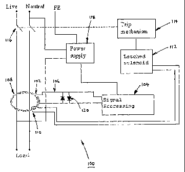
Referring now to the drawings, a residual current
device 100 according to the present invention is shown
schematically in Fig. 3, which utilises a VI architecture
CA 02649183 2008-10-21
WO 2007/116221 PCT/GB2007/001332
13
as a basis for such residual current device 100. In
addition, the RCD 100 includes VD detection electronics
for signal processing 104 and extra features. When the
line voltage falls below a predetermined threshold level
(typically 50V), the device 100 functions in VI mode, as
a conventional VI RCD with its inherent advantages. When
the line voltage is above the threshold level, the device
100 functions in VD mode, still using the VI toroidal
core 108, secondary winding 110 and tripping relay 112,
but allowing an electronic processor 104 to measure and
determine the tripping level and other ancillary
features, such as, for example, undervoltage release and
warning indication, etc.
In VD mode, when the power supply 118 is functioning,
the RCD 100 is in voltage dependent mode. The protection
winding 102 is connected to a low impedance within the
signal processor 104, so that any resultant residual
current causes current to flow in this winding 102. Any
current flowing in this winding 102 automatically
demagnetises the core 108. Therefore, the current
induced in the, generally, single turn secondary winding
110 will be much smaller than expected in a VI device and
so the latching solenoid 112, trip mechanism 114 and
contacts 116 do not operate. An alternative view of
this mechanism is that by having the advantage of more
turns, the protection winding 102 can be used to "steal"
current which would otherwise be induced in the single
turn secondary winding 110 and so VI operation is
effectively disabled. The current in the protection
winding 102 can be monitored by the signal processing
104, and used to offer other ancillary features.
CA 02649183 2008-10-21
WO 2007/116221 PCT/GB2007/001332
14
When in VD mode, and a residual fault condition is
detected, tripping of the device 100 can be initiated by
raising the impedance across the protection winding 102
to a high level, such that the winding 102 no longer
conducts current and the device resumes VI operation.
Since all the fault current is now induced in the
secondary trip winding 110, the solenoid 112 is operated
and the existing residual current supplies the energy to
achieve this. To ensure tripping occurs, it is also
possible to drive an AC current into the protection
winding 102, which will also induce current in the single
turn secondary winding 110, thereby effecting operation
of the solenoid 112, as discussed in further detail in
respect of Fig. 4.
In VI mode, when the signal processing circuit 104 is
not powered, the signal processing circuit 104 is
configured such that the impedance across the protection
winding 102 is high, so normal VI operation is unaffected
by the extra circuit components. Diodes 120 remain in
the protection circuit 106 for the purposes described in
relation to Fig. 2, (i.e. the prevention of permanent
magnetisation of the toroid 108). In normal VI and VD
modes of operation, the voltages across these diodes 120
are never high enough to cause them to conduct.
Fig. 4 shows further detail of the implementation of
the device set out schematically in Fig. 3, and shows
that the magnetic latch trip 212 is directly connected to
the secondary winding 206 on the toroid 202. Also on the
toroid 202 is the tertiary protection winding 204 of the
CA 02649183 2008-10-21
WO 2007/116221 PCT/GB2007/001332
standard VI RCD. Within the electronic circuitry stage
216, the signal induced into the tertiary winding 204 is
connected to a low impedance amplifier circuit 224.
When VD mode line voltage threshold is reached, the
amplifier 224 powers-up, via power supply 218, and the
input impedance is reduced to a very low level, in the
order of 152. As the tertiary protection winding 204 has
a much higher turns ratio than the secondary winding 206
and is terminated into a very low impedance, most of the
magnetic flux transformed by the toroidal core 202 will
result in most of the current flowing in the tertiary
winding 204. The current induced in the secondary
winding 206 will therefore be much smaller than normal
when in VI mode, and so the tripping relay 212 and
contacts 214 will not operate at normal levels when in VD
mode.
Tripping the device 200 in VD mode can also be
achieved by injecting a large current into the tertiary
winding 204, via trip signal generator 226, which is
transformed into a tripping current in the secondary
winding 206 by the sensor core 202 causing the tripping
relay 212 to release. This induced current is nominally
set to be of the order of 1 to 1.5 times the rated trip
current (IA). Generally, the size of the induced
tripping current is dependent on the sensor's 202
permeability and the construction of the tripping relay
212.
The skilled person will appreciate that the induced
tripping current should be consistent with the supply
frequency (i.e. AC 50Hz or 60Hz) and has to be broadly in
CA 02649183 2008-10-21
WO 2007/116221 PCT/GB2007/001332
16
phase with the fault current. It is also envisaged that
increasing the level of induced tripping current with
time could also overcome any minor stiction of the
tripping release 212. Clearly, it is better to trip the
relay 212 even if the trip time is out of specification
than not to trip at all in a dangerous situation.
Tripping the device 200 in VD mode can further be
achieved when the current imbalance flowing between the
primary conductors exceeds the predetermined current
imbalance simply by switching the low impedance amplifier
circuit 224 off (resulting in a high impedance) which
will cause the fault current to be induced in the
secondary winding 206. The resulting imbalance current
would be sufficient to cause the relay 212 to trip the
mechanism 214. A similar condition will exist in the
equivalent circuit described by Fig. 5, as described
below.
The frequency response of the device 200 shown in
Fig. 4 is largely determined by the toroidal current
sensor 202 whose performance is dependent on many
factors, including the influence of both the secondary
winding 206 inductance and the tertiary winding 204
inductance and the circuit impedance. The primary
inductance of the current sensor 202 is also important,
but, generally, the circuit impedance is so low it is of
little consequence.
Fig. 5 shows an equivalent circuit of the device 200
shown in Fig. 4 in VI mode. The component values are
CA 02649183 2008-10-21
WO 2007/116221 PCT/GB2007/001332
17
typical but can vary considerably for different ranges
and combinations of solenoids 212 and toroidal cores 202.
The equivalent circuit shown in Fig. 5 represents the
device 200 in VI mode, where the impedance across the
protection winding 204 is high. This is shown as a
burden resistance RX having an effective value of lOMS2 in
Fig. 5. As such, the VD circuit which connects to the
voltage dependent amplifier 224 and processing 220 is
essentially passive, and conducts no current I. This
represents the tertiary protection winding 204.
Therefore, all flux produced by a residual current in the
single turn primary winding is all coupled to the single
turn secondary winding 206 in the VI circuit and the
resulting current Is is conveyed to the solenoid 212 to
effect tripping. The solenoid 212 is represented by RS
and is typically about 152. In this case, it takes 10mA
to trip the solenoid 212.
The frequency response of the equivalent circuit of
Fig. 5 is shown in Fig. 6 for a residual current IA of
30mA. It is worth noting that the current IX in the
inductbr LX and hence in the tertiary protection circuit
204 is zero due to its high impedance, but the VI circuit
is carrying 9mA at 50Hz. This would not cause the
solenoid 212 to trip, even though for a 30mA breaker it
should disconnect the supply in this circumstance. This
is a problem in reality since the device is working on
the slope of the response and variations in core
materials or solenoid sensitivity can push the device out
of the required specification.
CA 02649183 2008-10-21
WO 2007/116221 PCT/GB2007/001332
18
To compensate for this, it is known to subject the
whole device 200 to a large variable magnetic field which
can modify the holding magnet in the solenoid 212 to
adjust its characteristics and, in this case, reduce its
tripping threshold from lOmA to 9mA. In use, it would be
better if the device 200 worked on the plateau of the
frequency response but this means more primary turns
which is difficult in practice since it consists of large
mains conductors. Instead the toroidal core 212 can be
made as big as possible to increase inductance.
Fig. 7 shows an equivalent circuit of the device 200
in VD mode. It is worth noting that the tertiary winding
204 now has a low value burden resistance RX of 1052 and
the voltage across this is measured to determine the
fault current I. Fig. 8 shows the frequency response of
the circuit shown in Fig. 7.
The current IX in the VD circuit is dominant and
reaches approximately the value it would if the VI
winding 206 was not present (i.e. a value of 1mA given
the 30:1 turns ratio). The response is also now flat and
predicable at 50Hz. The current IS in the VI circuit is
approximately 330pA and so too low to directly operate
the solenoid 212. This current is the cause of the lower
than expected current in the VD circuit and the error is
directly calculated from the turns ratio of the VI 206
and VD windings 204. In this case, there is a 30:1 ratio
so the VD circuit is 330pA/3OpA = 11uA lower than
expected. This error remains fairly constant and small
for variations in the core and so can be compensated.
CA 02649183 2008-10-21
WO 2007/116221 PCT/GB2007/001332
19
Note that at 50Hz, the response is now flat since the
current sensor 202 is much nearer to `true' current
transformer operation. This means material variations and
drift are not significant and calibration is not
necessary.
Fig. 9 shows the basic schematic arrangement of the
low impedance amplifier 224 connected to the circuit
protection winding 204 shown in Fig. 4, and depicts one
approach using operational amplifiers U1 and U2 to
effectively alter the input impedance seen by the circuit
protection winding 204.
As shown in Fig. 9, U2 buffers the voltage reference
Vref that is used subsequently as the reference for the
low impedance amplifier 224 (i.e., U2 is not turned on
until the line voltage exceeds a changeover threshold).
Vref is the internal reference of the measurement system
and its level is mid-rail between Agnd and the analogue
supply. Current induced in the protection winding 204 is
applied to Rburden and the developed voltage is applied to
the input terminal of U1. Rgain sets the amplifier gain and
Vout is applied to the measurement system, i.e. the signal
processor 220 of Fig. 4.
The main source of errors is the offset voltage
developed in U1. Without compensation, the offset
voltages would obliterate the voltage developed across
Rburden= To overcome this limitation the amplifier has to
be of a low offset design preferably of an auto-zeroing
type. In Fig. 9, Rburden is shown as a single resistance.
CA 02649183 2008-10-21
WO 2007/116221 PCT/GB2007/001332
In practice, this is composed of the burden resistance
and any switch resistance present in the circuit.
When the device is operating in voltage independent
mode, U1 and U2 are turned of f and the input impedance
rises to the order of several M.
However, if small surge currents are present these
could cause the relay to actuate so causing nuisance
tripping. To improve the susceptibility to nuisance
tripping due to surge currents, two options have been
considered. This firstly could be achieved by reducing
the value of Rburden= In reality, this is difficult to
achieve, as physically implementing a small resistance
with a low tolerance is difficult either in a discrete
solution or as part of a silicon implementation of the
electronic circuitry 216. In silicon, the low resistance
is determined by any switch resistance in the circuit
path and the physical size of the resistance when
implemented on the silicon substrate. In practical terms,
the minimum resistance is typically 100.
The second option is to increase the turns ratio of
the protection winding 204. This effectively lowers the
resistance of Rburden = The maximum number of turns is
dependent on the following factors: (i) physical space
in the device; (ii) toroidal core material (and its
effect on permeability); (iii) diameter of the line and
neutral conductors; and (iv) resistance of the trip
relay. Typically, the turns ratio is unlikely to exceed
100, because of any one or more of the listed factors.
CA 02649183 2008-10-21
WO 2007/116221 PCT/GB2007/001332
21
Considering the architecture of the devices described
above, the person skilled in the art will appreciate that
there a number, of factors that determine the mode of
operation of the device: -
(i) Electronics start-up time - any electronic
circuit requires a finite time for the power supply to
stabilise and the measurement system to initialise. In
practice, this can be in the range of 5 to 10ms depending
on the line voltage, and hence how much current the power
supply can draw to start up. EN/IEC 61008 requires the
device to respond to a gross fault >5IA or >500A within
40ms. While this could be achieved using the VD
electronics 216 in the time available (<30ms), it is more
advantageous to allow the VI circuit 206, 212 to handle
gross faults. Therefore, at start up and at UL >
Changeover limit, a 40ms delay is added to ensure a
smooth transition from VI mode to VD mode.
(ii) Supply voltage - all electronic RCDs require a
minimum level of supply voltage to function, typically in
the order of BOV, although some devices can operate down
to 50V. It can be argued that below 50V there is a
reduced hazard of electric shock, but there is always the
potential for a residual current fault which electronic
RCD devices could not protect against.
(iii) Electronic failure - All mechanical and
electronic RCDs have a finite lifetime which is usually
determined by the types of components used in
construction and the operational environment. Using
CA 02649183 2008-10-21
WO 2007/116221 PCT/GB2007/001332
22
reliability models compatible with IEC 61508, it can be
determined that the two main failure modes are
(a) Failure to detect; and (b) Failure to trip.
As mentioned above there are two fault scenarios that
will prevent the device operating correctly in VD mode,
`Failure to detect' and `Failure to trip'. The
electronic circuit 216 connected to the protection
circuit 208, is composed of three essential circuit
blocks, namely the power supply 218; the low impedance
amplifier 224 and the signal processor 220.
Any failure of the power supply 218 will cause the
low impedance amplifier 224 to turn off and the RCD 200
will therefore return to VI mode. As shown in Fig. 4,
the low impedance amplifier 224 and the signal processor
220 are connected by a serial interface used for
configuration and signal selection. The serial port in
the low impedance amplifier 224 is connected to a
watchdog timer 228 which is reset with every serial
transmission. If the processor 220 stops or executes a
programme abnormally, the serial transmission will stop
and the watchdog timer 228 will timeout returning the
device to VI mode. The timeout period is programmable
but is typically <40ms. This ensures that even when a
gross earth fault occurs simultaneous with an electronics
failure (double fault), the device 200 will trip within
the specified time by returning to VI mode.
The signal processor 220 also has a similar watchdog
timer 222 which is able to reset the signal processor 220
and restart its operation should the programme execute
CA 02649183 2008-10-21
WO 2007/116221 PCT/GB2007/001332
23
abnormally or stop. In this case, the serial transmission
will stop momentarily and the low impedance amplifier 224
will return to VI mode, while the reset operation takes
place.
The skilled person will therefore appreciate that
each main circuit block can initiate a hardware-based
operation to return the RCD 200 to VI mode, should an
electronics failure occur.
Table 1 summarises the operational state of the RCD
200 under various operating conditions.
Switch Switch UL < UL > Electronic
on on + Changeover Changeover failure
Tstart limit limit
VI X X X
VD X X
Table 1
Switch on
At switch on, whilst the power supply stabilises, the
device 200 operates in a VI manner using the RCD sensor's
single turn secondary winding 206 and the trip relay 212.
At this time, the performance of the device is largely
governed by the permeability of the sensor core 202 and
the performance of the trip relay 212. If there are
large earth leakage currents at start up, these will be
detected by the VI circuit 202, 206 causing the trip
mechanism 212 to open the contacts 214.
CA 02649183 2008-10-21
WO 2007/116221 PCT/GB2007/001332
24
Switch on + Tgtart
Once the line voltage has reached or exceeded the
minimum operating voltage, the power supply 218 starts
and the low impedance amplifier 224 and the signal
processor 220 initialise. The low impedance amplifier
224 is not turned on until the line voltage exceeds a
changeover threshold. At this time, the amplifier input
impedance is reduced to almost 00 and any flux in the
toroidal core 202 will be diverted to induce a current
principally in the tertiary winding 204. The changeover
voltage is always higher than the minimum operating
voltage, in order to ensure a reliable and repeatable
transition from VI mode to VD mode.
Uz < Changeover limit
During operation in VD mode, if the line voltage UL
falls below the changeover limit, the input amplifier U1
is turned off into a high impedance state, therefore
returning the device 200 to VI mode.
UL > Changeover limit
This is a similar situation as described in Switch on
+ Tstart = The power supply 218 is active but the line
voltage UL has previously been below the changeover limit.
Once the line voltage exceeds the changeover limit, the
input amplifier U1 is turned on and the input impedance
is reduced to almost 00 and any flux in the core 202 will
be diverted to induce a current in the tertiary winding
CA 02649183 2008-10-21
WO 2007/116221 - PCT/GB2007/001332
204. Note it is not necessary for the changeover limit
to be at the same level in both of the previous cases,
indeed it may be more advantageous for the limit to be
higher in the second case to prevent continuous changes
from VI to VD modes at the lower UL < changeover limit.
Fig. 10 shows the processing algorithm used to
determine the changeover between VI mode and VD modes.
The software uses a number of event timers and
associated interrupts to process different activity
streams. The main point to note is the use of two
filters to process the voltage measurements. The slow
filter is used for accurate voltage measurement if
required by the RCD. The fast filter is solely for
determining if the changeover between VI and VD modes is
required. The left-hand side of Fig. 10 is performed
every 330ps (60 samples per cycle), while the right-hand
side is performed every 1/2 cycle (10ms), so the fast
signal capture is performed with a sampling frequency of
around 2.6Khz, while the decision to switch to VI mode is
performed every 1/2 cycle.
Referring to the left-hand side of Fig. 10, every
330us (block 300) the line and neutral data is captured
302. The line and neutral channels ideally need to
sampled simultaneously, however, in a practical device,
these can be sampled in successive acquisitions. For a
multi-phase device, the skilled person will appreciate
that the same sampling order must be maintained.
At blocks 304 and 306, the neutral is subtracted from
the line voltage and the mean squared of the line to
CA 02649183 2008-10-21
WO 2007/116221 PCT/GB2007/001332
26
neutral voltage is calculated. At blocks 308 and 310,
the new measurement value is pushed into the fast and
slow filters. The product of the fast filter is then
applied to a peak detector 312 to evaluate the maximum
value of the line to neutral voltage.
Every lOms (block 320), the peak detector is
evaluated 322 to determine if it has breached the minimum
or maximum changeover threshold by converting the mean
squared line to neutral voltage to a root mean squared
value. At blocks 324 and 326, a comparison of the RMS
line to neutral voltage to the changeover limit is made.
If the RMS line to neutral voltage is below the
changeover limit, the device is switched to VI mode 328.
At this point, the amplifier circuit 224 is
turned-off, thereby setting the input impedance high. If
the RMS line to neutral voltage is above the changeover
limit, the device is switched to VD mode 330 by turning
on amplifier 224, thereby setting the input impedance
low. At block 332, the peak detector is reset and rests
for the next 1/2 cycle.
Electronic failure
Any failure of the electronic circuit 216 connected
to the protection circuit 208 will cause the low
impedance amplifier 224 to turn off and the RCD 200 will
therefore return to VI mode, as noted above.
Fig. 11 shows the general arrangement of an
alternative embodiment of the present invention.
CA 02649183 2008-10-21
WO 2007/116221 PCT/GB2007/001332
27
In recent years, an alternative VI structure has been
available, whereby a high-impedance tripping relay 230
has been used in conjunction with a delay circuit 232.
The purpose of this approach is to reduce the VI
circuit's 206, 212 susceptibility to surge/impulse
currents that could cause false tripping with the
embodiment of Fig. 4. This construction has been
incorporated in the present invention; the main
difference between the embodiment of Fig. 4 and that set
out in Fig. 11 is the manner in which the tripping relay
230 is actuated. Since the turns ratio of high-impedance
tripping relay 230 is higher it is more advantageous to
drive the relay 230 directly from the electronics 216
when in VD Mode.
In VI mode, the actuator drive and the input
amplifier is in a high impedance state, any induced fault
current is applied to the delay circuit 232 and
subsequently to the tripping relay 230 in the
conventional manner. When the line voltage is above the
VD mode threshold, the detection and measurement
electronics 216 is turned on and the input amplifier is
in a low impedance state, and the circuit responds in the
same way as previously described. When the tripping
relay 230 is required to operate, an actuator port on the
signal processor 220 drives current directly into the
trip relay 230 causing it to open. The actuator port is
an I/0 port on the signal processor 220 used to trip the
magnetic latch relay 230 in a high-impedance
configuration. The port only requires low voltage (3 to
5V) and limited current (up to 10mA) capacity to trip a
CA 02649183 2008-10-21
WO 2007/116221 PCT/GB2007/001332
28
typical relay 230. The port should also be
tri-state capable, for when operating in VI mode.
The significant improvement with this embodiment, is
the increase in available current to activate the
tripping relay 230. In VI mode, this current is
typically in the order of 400pA, whilst in VD mode, this
can be in the order of several mA. This increased
current may help to improve the reliability of the
tripping relay 230, if the relay has only minor
`stiction'.
Various alterations and modifications may be made to
the present invention without departing from the scope of
the invention. For example, although particular
embodiments refer to implementing the present invention
on a single phase electrical installation, this is in no
way intended to be limiting. as, in use, the present
invention can be incorporated into larger installations,
both single and multi-phase.