Note: Descriptions are shown in the official language in which they were submitted.
CA 02649505 2014-03-17
TELECOMMUNICATIONS JACK WITH CROSSTALK COMPENSATION PROVIDED ON A
MULTI-LAYER CIRCUIT BOARD
Technical Field
The present invention relates generally to telecommunications equipment. More
particularly, the present invention relates to telecommunications jacks that
are configured to
compensate for near end crosstalk.
Background
In the field of data communications, communications networks typically utilize
techniques designed to maintain or improve the integrity of signals being
transmitted via the
network ("transmission signals"). To protect signal integrity, the
communications networks
should, at a minimum, satisfy compliance standards that are established by
standards
committees, such as the Institute of Electrical and Electronics Engineers
(IEEE). The compliance
standards help network designers provide communications networks that achieve
at least
minimum levels of signal integrity as well as some standard of compatibility.
One prevalent type of communication system uses twisted pairs of wires to
transmit
signals. In twisted pair systems, information such as video, audio and data
are transmitted in
the form of balanced signals over a pair of wires. The transmitted signal is
defined by the
voltage difference between the wires.
Crosstalk can negatively affect signal integrity in twisted pair systems.
Crosstalk is
unbalanced noise caused by capacitive and/or inductive coupling between wires
and a twisted
pair system. The effects of crosstalk become more difficult to address with
increased signal
frequency ranges.
1
CA 02649505 2008-10-10
WO 2007/120668
PCT/US2007/008847
= The effects of crosstalk also increase when transmission signals are
positioned closer to one another. Consequently, communications networks
include
areas that are especially susceptible to crosstalk because of the proximity of
the
transmission signals. In particular, communications networks include
connectors
that bring transmission signals in close proximity to one another. For
example, the
contacts of traditional connectors (e.g., jacks and plugs) used to provide
interconnections in twisted pair telecommunications systems are particularly
susceptible to crosstalk interference.
Figure 1 shows a prior art panel 20 adapted for use with a twisted pair
telecommunications system. The panel 20 includes a plurality of jacks 22. Each
jack 22 includes a port 24 adapted to receive a standard telecommunications
plug 26.
Each of the jacks 22 is adapted to be terminated to four twisted pairs of
transmission
wires. As shown at Figure 2, each of the jacks 22 includes eight contact
springs
labeled as having positions 1-8. In use, contact springs 4 and 5 are connected
to a
first pair of wires, the contact springs 1 and 2 are connected to a second
pair of
wires, contact springs 3 and 6 are connected to a third pair of wires, and
contact
springs 7 and 8 are connected to a fourth pair of wires. As shown at Figure 3,
a
typical plug 26 also has eight contacts (labeled 1-8) adapted to interconnect
with the
corresponding eight contacts of the jack 22 when the plug is inserted within
the port
24.
To promote circuit density, the contacts of the jacks and the plugs are
required to be positioned in fairly close proximity to one another. Thus, the
contact
regions of the jacks and plugs are particularly susceptible to crosstalk.
Furthermore,
certain pairs of contacts are more susceptible to crosstalk than others. For
example,
the first and third pairs of contacts in the plugs and jacks are typically
most
susceptible to crosstalk.
To address the problems of crosstalk, jacks have been designed with
contact spring configurations adapted to reduce the capacitive coupling
generated
between the contact springs so that crosstalk is minimized. An alternative
approach
involves intentionally generating crosstalk having a magnitude and phase
designed
to compensate for or correct crosstalk caused at the plug or jack. Typically,
crosstalk compensation can be provided by manipulating the positioning of the
contacts or leads of the jack or can be provided on a circuit board used to
electrically
2
CA 02649505 2014-03-17
connect the contact springs of the jack to insulation displacement connectors
of the jack.
The telecommunications industry is constantly striving toward larger signal
frequency
ranges. As transmission frequency ranges widen, crosstalk becomes more
problematic. Thus,
there is a need for further development relating to crosstalk remediation.
Summary
One aspect of the present disclosure relates to circuit board layering
configurations
adapted for supporting the effective compensation of crosstalk in a
telecommunications jack.
Another aspect of the present disclosure relates to the use of high impedance
lines to
compensate for return loss caused by crosstalk compensation arrangements.
Still another aspect of the present disclosure relates to the use of
capacitive couplings
to overcome return loss issues caused by crosstalk compensation arrangements.
Still another aspect of the present disclosure relates to crosstalk
compensation
arrangements and methods for designing crosstalk compensation arrangements.
In accordance with an aspect of the invention, there is provided a
telecommunications
jack comprising:
a housing defining a port for receiving a plug;
a plurality of contact springs adapted to make electrical contact with the
plug when the
plug is inserted into the port of the housing;
a plurality of wire termination contacts for terminating wires to the jack;
a circuit board that electrically connects the contact springs to the wire
termination
contacts, the circuit board including first and second conductive layers
separated by a first
dielectric layer, the first dielectric layer having a thickness less than .01
inches; and
the first and second conductive layers including a cross talk compensation
arrangement
including spaced-apart capacitor members, the capacitor members being
separated by the first
dielectric layer.
In accordance with another aspect of the invention, there is provided a
telecommunications jack adapted to receive a plug, the telecommunications jack
having a
compensation arrangement that compensates for cross talk generated at the
plug, the
telecommunications jack comprising:
3
CA 02649505 2014-03-17
a housing defining a port for receiving the plug;
first, second, third, fourth, fifth, sixth, seventh and eighth consecutively
arranged
contact springs adapted to make electrical contact with the plug when the plug
is inserted into
the port of the housing;
first, second, third, fourth, fifth, sixth, seventh and eighth wire
termination contacts for
terminating wires to the jack;
a circuit board including first, second, third, fourth, fifth, sixth, seventh
and eighth
tracings that respectively electrically connect the first, second, third,
fourth, fifth, sixth,
seventh and eighth contact springs to the first, second, third, fourth, fifth,
sixth, seventh and
eighth wire termination contacts, the circuit board including first and second
conductive layers
separated by a first dielectric layer, the first dielectric layer having a
thickness less than
.01 inches; and
a first compensation zone provided at the first and second conductive layers,
the first
compensation zone including first opposing capacitor plates providing a first
capacitive
coupling, the first capacitive coupling being made between the third and fifth
tracings, the first
opposing capacitor plates being separated by the first dielectric layer, the
first compensation
zone also including second opposing capacitor plates providing a second
capacitive coupling,
the second capacitive coupling being made between the fourth and sixth
tracings, the second
opposing capacitor plates being separated by the first dielectric layer;
a second compensation zone provided at the first and second conductive layers,
the
second compensation zone including third opposing capacitor plates providing a
third
capacitive coupling, the third capacitive coupling being made between the
third and fourth
tracings, the third opposing capacitor plates being separated by the first
dielectric layer, the
second compensation zone also including fourth opposing capacitor plates
providing a fourth
capacitive coupling, the fourth capacitive coupling being made between the
fifth and sixth
tracings, the fourth opposing capacitor plates being separated by the first
dielectric layer; and
a third compensation zone providing a fifth capacitive coupling and a sixth
capacitive
coupling, the fifth capacitive coupling being made between the third and fifth
tracings, and the
sixth capacitive coupling being made between the fourth and sixth tracings.
3a
CA 02649505 2014-03-17
Still another aspect of the invention concerns a telecommunications jack
comprising:
a housing defining a port for receiving a plug;
a plurality of contact springs adapted to make electrical contact with the
plug when the
plug is inserted into the port of the housing;
a plurality of wire termination contacts for terminating wires to the jack;
a circuit board that electrically connects the contact springs to the wire
termination
contacts, the circuit board including a first side defined by a first outer
conductive layer and a
second side defined by a second outer conductive layer, the circuit board also
including an
intermediate conductive layer, the first outer conductive layer being
separated from the
intermediate conductive layer by a first dielectric layer, the second outer
conductive layer
being separated from the intermediate conductive layer by a second dielectric
layer, the
second dielectric layer having a greater thickness than the first dielectric
layer;
the first and second conductive layers including a cross talk compensation
arrangement
including first spaced-apart capacitor members, the first spaced-apart
capacitor members
being separated by the first dielectric layer; and
the contact springs being mounted at the first side of the circuit board and
the wire
termination contacts being mounted at the second side of the circuit board.
A variety of additional inventive aspects will be set forth in the description
that follows.
The inventive aspects can relate to individual features and to combinations of
features. It is to
be understood that both the foregoing general description and the following
detailed
description are exemplary and explanatory only and are not restrictive of the
broad inventive
concepts upon which the embodiments disclosed herein are based.
Brief Description of the Drawings
Figure 1 is a perspective view of a prior art telecommunications panel;
Figure 2 is a schematic illustration of a prior art jack;
3b
CA 02649505 2008-10-10
WO 2007/120668
PCT/US2007/008847
Figure 3 is a schematic representation of a prior art
telecommunications plug;
Figure 4 is a front, perspective view of a telecommunications jack
having features that are examples of inventive aspects in accordance with the
principles of the present disclosure;
Figure 5 is an exploded view of the jack of Figure 4;
Figure 6 is a side view of the circuit board, insulation displacement
connectors and contact springs of the telecommunications jack of Figure 4;
= Figure 7 is a front view of the circuit board, contact springs and
insulation displacement connectors of Figure 6;
Figure 8 is a top view of the circuit board and contact springs of
Figure 6;
Figure 9 is a cross-sectional view taken along section line 9-9 of
Figure 8;
Figure 10 is a schematic diagram showing a crosstalk compensation
scheme incorporated into the telecommunications jack of Figure 4;
Figure 11 is a schematic diagram showing a compensation
arrangement used to provide crosstalk compensation between the 4-5 and 3-6
pairs
of the telecommunications jack of Figure 4;
Figure 12 is a schematic vector diagram showing a compensation
arrangement used to provide crosstalk compensation between the 1-2 and 3-6
pairs
of the telecommunications jack of Figure 4;
Figure 13 is a graph that depicts how certain factors can affect return
loss in the jack of Figure 4 across a range of frequencies;
Figure 14 is a tracing overlay view of the circuit board used in the
telecommunications jack of Figure 4;
Figure 15 shows a front conductive layer of the circuit board used in
the telecommunications jack of Figure 4;
Figure 16 shows a middle conductive layer of the circuit board used
in the telecommunications jack of Figure 4; and
Figure 17 is shows a back conductive layer of the circuit board used
in the telecommunications jack of Figure 4.
4
CA 02649505 2008-10-10
WO 2007/120668 PCT/US2007/008847
Detailed Description
Figures 4 and 5 show a telecommunications jack 120 (i.e., a
telecommunications connector) having features that are examples of inventive
aspects in accordance with the principles of the present disclosure. The jack
120
includes a dielectric housing 122 having a front piece 124 and a rear piece
126. The
front and rear pieces 124, 126 can be interconnected by a snap fit connection.
The
front piece 124 defines a front port 128 sized and shaped to receive a
conventional
telecommunications plug (e.g., an RJ style plug such as an RJ 45 plug). The
rear
piece 126 defines an insulation displacement connector interface and includes
a
plurality of towers 130 adapted to house insulation displacement connector
blades/contacts. The jack 120 further includes a circuit board 132 that mounts
between the front and rear pieces 124, 126 of the housing 122. A plurality of
contact springs CS1-CS8 are terminated to a front side of the circuit board
132. A
plurality of insulation displacement connector blades IDC1-IDC8 are terminated
to a
back side of the circuit board 132. The contact springs CS1-CS8 extend into
the front
port 128 and are adapted to be electrically connected to corresponding
contacts
provided on a plug when the plug is inserted into the front port 128. The
insulation
displacement connector blades IDC1-IDC8 fit within the towers 130 of the rear
piece
126 of the housing 122. The circuit board 132 has tracks T1-T8 (e.g.,
tracings, see
Figures 14-17) that respectively electrically connect the contact springs CS1-
CS8to
the insulation displacement connector blades IDC1-IDC8.
In use, wires are electrically connected to the contact springs CS I-CS8
by inserting the wires between pairs of the insulation displacement connector
blades
= IDC1-IDC8. When the wires are inserted between pairs of the insulation
displacement connector blades IDC1-IDC8, the blades cut through the insulation
of
the wires and make electrical contact with the center conductors of the wires.
In this
way, the insulation displacement connector blades IDC1-IDC8, which are
electrically
connected to the contact springs CS1-CS8 by the tracks on the circuit board,
provide
an efficient means for electrically connecting a twisted pair of wires to the
contact
springs CS1-CS8 of the jack 120.
The contact springs CSI-CS8are shown more clearly in Figures 6-8.
The relative positioning, shape and curvature of the contact springs CS I-
CS8is
preferably adapted to provide some initial crosstalk compensation at the jack
120.
5
CA 02649505 2008-10-10
WO 2007/120668 PCT/US2007/008847
The circuit board 132 of the jack 120 is preferably a multiple layer
circuit board. For example, Figure 9 shows the circuit board 132 including a
first
conductive layer 140, a second conductive layer 142 and a third conductive
layer
144. The first and second conductive layers 140, 142 are separated by a first
dielectric layer 146. The second and third conductive layers 142, 144 are
separated
by a second dielectric layer 148. The first conductive layer 140 is located at
a front
side of the circuit board 132 and the third conductive layer 144 is located at
a back
side of the circuit board 132. The contact springs CS i-CS8are mounted at the
front
side of the circuit board 132, while the insulation displacement connector
blades
IDCI-IDC8 are mounted at the back side of the circuit board 132. Vias extend
through the first and second dielectric layers 146, 148 to provide electrical
connections between the conductive layers 140, 142 and 144. The conductive
layers
140, 142 and 144 are defined by electrically the conductive tracks T1-T8 (see
Figures
14-17). The tracks T1-T8 are formed (e.g., etched or otherwise provided) on
the
dielectric layers 146, 148.
The circuit board 132 preferably includes structures for compensating
for near end crosstalk that occurs at the jack/plug interface. In certain
embodiments,
the structures for compensating for near end crosstalk include capacitive
couplings
provided between the first and second conductive layers 140, 142. In preferred
embodiments, the capacitive couplings are provided by sets of opposing,
generally
parallel capacitive plates located at the first and second conductive layers
140, 142.
To increase the magnitude of the capacitive coupling provided between the
capacitive plates of the first and second conductive layers 140, 142, it is
desirable
for the first dielectric layer 146 to be relatively thin. For example, in
certain
embodiments the first dielectric layer 146 can have a thickness ti less than
about .01
inches, or less than about .0075 inches, or less than about .005 inches, or
less than
.003 inches. In other embodiments, the thickness t1 can be in the range of
.001
inches to .003 inches or in the range of .001 inches to .005 inches. In a
preferred
embodiment, the thickness t1 is about .002 inches.
In certain embodiments, the first dielectric layer 146 can be made of a
material having a relatively low dielectric constant. As used herein,
dielectric
constants are dielectric constants relative to air. In certain embodiments,
the
dielectric constant of the first dielectric layer 146 can be equal to or less
than about
5. In other embodiments, the dielectric constant of the first dielectric layer
146 can
6=
CA 02649505 2008-10-10
WO 2007/120668
PCT/US2007/008847
be less than or equal to about 4 or less than or equal to about 3. An example
material for manufacturing the first dielectric layer 146 is a flame resistant
4 (FR-4)
circuit board material. FR-4 circuit board material is a composite of a resin
epoxy
reinforced with a woven fiberglass mat.
The second dielectric layer 148 is preferably configured to isolate the
third conductive layer 144 from the first and second conductive layers 140,
142.
The second dielectric layer 148 can have a different thickness t2 than the
thickness ti
of the first dielectric layer 146. In certain embodiments, the second
dielectric layer
148 is at least 2.5 times thicker than the first dielectric layer 146 or at
least five
times thicker than the first dielectric layer 146. In still other embodiments,
the
second dielectric layer 148 is at least 10 times or at least 20 times thicker
than the
first dielectric layer 146. In one example embodiment, the thickness t2 of the
second
dielectric layer 148 is in the range of .050 inches to .055 inches. In another
example
embodiment, the thickness t2 of the second dielectric layer 148 is in the
range of
.040 inches to .050 inches.
The second dielectric layer 148 can also be manufactured of a
= different material as compared to the first dielectric layer 146. In
certain
embodiments, the second dielectric layer can have different dielectric
properties as
compared to the first dielectric layer 146. For example, in certain
embodiments the
first dielectric layer 146 can have a dielectric constant that is greater
(e.g., at least
1.5 times or at least 2 times greater) than the dielectric constant of the
second
dielectric layer 148. In one example, the second dielectric layer 148 can be
manufactured of a material such as FR-4. Of course, it will be appreciated
that other
materials could also be used.
The circuit board 132 includes a number of capacitive couplings
having magnitudes and locations adapted to compensate for near end crosstalk.
Near end crosstalk is most problematic between the 4-5 and 3-6 pairs. To
compensate for near end crosstalk between the 4-5 and 3-6 pairs, three
interdependent zones of compensation are used between tracks T4_5 and tracks
T3-6-
.
As shown at Figure 10, the three interdependent zones of compensation include
a
first zone of compensation ZA1, a second zone of compensation ZA2 and a third
zone
of compensation ZA3. The first zone of compensation ZAI includes a capacitive
coupling Cl between track T3 and track T5, and a capacitive coupling C2
between
track T4 and track T6. The second zone of compensation ZA2 includes a
capacitive
7
CA 02649505 2008-10-10
WO 2007/120668 PCT/US2007/008847
coupling C3 between track T3 and track T4, and a capacitive coupling C4
between
track T5 and track T6. The third zone of compensation ZA3 includes a
capacitive
coupling C5 between track T3 and track T5, and a capacitive coupling C6
between
track T4 and track T6-
Figure 11 is a schematic diagram representative of the compensation
arrangement used to provide crosstalk compensation between the 4-5 and 3-6
pairs.
As shown at Figure 11, the compensation arrangement includes a first vector
100, a
second vector 102, a third vector 104, and a fourth vector 106. The first
vector 100
and the third vector 104 have positive polarities, while the second vector 102
and the
fourth vector 106 have negative polarities. The first vector 100 has a
magnitude of
M and corresponds to crosstalk introduced at the plug. The second vector 102
has a
magnitude of-3M and corresponds to crosstalk introduced at the first zone of
compensation ZA . The third vector 104 has a magnitude of 3M and corresponds
to
crosstalk introduced at the second zone of compensation ZA2. The fourth vector
106
has a magnitude of ¨M and corresponds to crosstalk introduced at the third
zone of
compensation ZA3. It will be appreciated that each vector is a lump sum of the
total
crosstalk provided at each respective compensation zone, with the vectors
being
placed at the centers or midpoints of the compensation zones.
In designing the compensation scheme of Figure 11, a number of
factors are taken into consideration when determining the placement of the
compensation zones. One factor includes the need to accommodate signal travel
in
both directions (i.e., in forward and reverse directions) through the tracks
on the
circuit board. To accommodate forward and reverse transmissions through the
circuit board, the compensation scheme preferably has a configuration with
forward
and reverse symmetry. It is also desirable for the compensation scheme to
provide
optimized compensation over a relatively wide range of transmission
frequencies.
For example, in one embodiment, performance is optimized for frequencies
ranging
from 1 MHz to 500 MHz. It is further desirable for the compensation
arrangement
to take into consideration the phase shifts that occur as a result of the time
delays
that take place as signals travel between the zones of compensation.
To minimize the effect of phase shift in the compensation
arrangement, it is preferred for the second vector 102 to be positioned as
close as
possible to the first vector 100. In Figure 11, the time delay between the
first vector
100 and the second vector 102 is shown as x. In one example embodiment, x can
be
8
CA 02649505 2008-10-10
WO 2007/120668
PCT/US2007/008847
= about 100 picoseconds for a signal having a transmission speed of 3X10⁸
meters per
second.
To maintain forward and reverse symmetry, it is preferred for the
time delay between the third vector 104 and the fourth vector 106 to be
approximately the same as the time delay between the first vector 100 and the
second vector 102. As shown in Figure 11, the time delay between the third and
fourth vectors is depicted as x.
The time delay y between the second vector 102 and the third vector
104 is preferably selected to optimize the overall compensation effect of the
compensation scheme over a relatively wide range of frequencies. By varying
the
time delay y between the second vector 102 and the third vector 104, the phase
angles of the first and second compensation zones are varied thereby altering
the
amount of compensation provided at different frequencies. In one example
embodiment, to design the time delay y, the time delay y is initially set with
a value
generally equal to x (i.e., the time delay between the first vector 102 and
the second
vector 104). The system is then tested or simulated to determine if an
acceptable
level of compensation is provided across the entire signal frequency range
intended
to be used. If the system meets the crosstalk requirements with the value y
set equal
to x, then no further adjustment of the value y is needed. If the compensation
scheme fails the crosstalk requirements at higher frequencies, the time delay
y can
be shortened to improve performance at higher frequencies. If the compensation
scheme fails the crosstalk requirements at lower frequencies, the time delay y
can be
increased to improve crosstalk performance for lower frequencies. It will be
appreciated that the time delay y can be varied without altering forward and
reverse
symmetry.
It has been determined that when magnitudes of the second and third
vectors 102, 104 are respectively -3M and 3M , the distance y is preferably
greater
than the distance x to provide optimized crosstalk compensation. However, if
the
magnitudes of the vectors 102, 104 are reduced below -3M and 3M(e.g., to -2.7M
and 2.7M), the distance y is preferably less than the distance x to provide
optimized
crosstalk compensation.
Crosstalk can also be an issue between the 1-2 and 3-6 pairs.
Particularly, substantial crosstalk can be generated between track T2 and
track T3.
As shown at Figure 10, a two-zone compensation arrangement is used to
compensate
9
CA 02649505 2008-10-10
WO 2007/120668 PCT/US2007/008847
for this crosstalk. The two-zone compensation arrangement includes a first
zone of
compensation Zgi and a second zone of compensation Zg2. The first zone of
compensation Zgi includes a capacitive coupling C7 between track Ti and track
T3,
and a capacitive coupling C8 between track T2 and track T6. The second zone of
compensation Zg2 includes a capacitive coupling C9 between track Ti and track
T6.
Figure 12 is a schematic vector diagram showing the compensation arrangement
used between the 1-2 and 3-6 pairs. As shown at Figure 12, three crosstalk
vectors
are taken into consideration. The first crosstalk vector 110 is representative
of
crosstalk generated at the plug. A second vector 112 is representative of
crosstalk
provided at the first compensation zone Zgi. The third vector 114 is
representative
of crosstalk generated at the second compensation zone Zg2. The first and
third
vectors 110, 114 have positive polarities and magnitudes of about N. The
second
vector 112 has a negative polarity and a vector about 2N. In testing the
compensation arrangement provided between tracks 1-2 and 3-6, it was
determined
that improved results were obtained when no discrete capacitive coupling was
provided between the track T2 and track T3 at the second zone of compensation
42.
However, in alternative embodiments, a discrete capacitive coupling can also
be
provided between track T2 and track T3 to maintain symmetry. It will be
appreciated
that M (shown at Figure 11) is typically substantially greater in magnitude
than N
(shown at Figure 12).
A two-zone compensation arrangement can be also be used to
provide crosstalk compensation between the 4-5 and 7-8 pairs. For example,
Figure
10 depicts a first zone of compensation Zci and a second zone of compensation
Zc2
providing compensation between the 4-5 and 7-8 pairs. The first zone of
compensation Zci includes a capacitive coupling CIO between track T8 and track
T5.
The second zone of compensation Z22 includes a capacitive coupling C11 between
tracks 8 and 4. The first and second zones of compensation Zci and Z2 can have
a
1-2-1 magnitude sequence similar to the two-zone compensation arrangement
described with respect to tracks 1-2 and 3-6.
In addition to the multiple zone compensation arrangements
described above, a number of single zone compensations can also be used. For
example, zone ZDI is a single zone compensation including a capacitive
coupling
C12 provided between track T2 and track T5. Another single zone compensation
ZEI
is provided by a capacitive coupling C13 formed between track T6 and track T8-
CA 02649505 2008-10-10
WO 2007/120668 PCT/US2007/008847
Another capacitive coupling C14 between track T5 and track T6 compensates for
unintended crosstalk generated within the board itself.
To address the crosstalk issue between the 4-5 and 3-6 pairs, a
relatively large amount of capacitance is used. This large amount of
capacitance can
cause the jack to have unacceptable levels of return loss. A number of methods
can
be used to improve return loss performance. For example, return loss
performance
can be improved by increasing the impedance of tracks T3, T4, T5 and T6 of the
board. The impedance of the tracks is preferably increased through the first,
second
and third zones of compensation, and also after the first, second, and third
zones of
compensation. The impedance can be increased by minimizing the transverse
cross
sectional area of tracks T3, T4, T5 and T6. An example transverse cross-
sectional
area of the tracks is in the range of 13 to 16 square mils (1 mil =.001
inches). The
impedance can also increase by routing the tracks so as to maintain a
relatively large
spacing between tracks T3 and T4 and between tracks T5 and T6. In one
embodiment, the impedance of the tracks T3-T6 is greater than 100 Ohms. In
another embodiment, the impedance is equal to or greater than 120 Ohms. In
still
another embodiment, the impedance of the tracks T3-T6 is equal to or greater
than
150 Ohms. In still a further embodiment, the impedance of the tracks T3-T6 is
equal
to or greater than 175 Ohms. In a further embodiment, the impedance of the
tracks
T3-T6 is equal to or greater than 200 Ohms.
The impedance of tracks T3-T6 can also be increased by increasing
the lengths of the tracks T3-T6 provided between the springs CS3-CS6 and the
insulation displacement connectors IDC3-IDC6. In certain embodiments, this
increased length can be provided by using serpentine or loop back routing
configurations for the tracks T3-T6. In lengthening the tracks T3-T6 provided
between contact springs CS3-CS6 and their corresponding insulation
displacement
connector blades IDC3-IDC6, in certain embodiments, the tracks T3-T6 can be
lengthened to be at least one and a half times or at least two times as long
as the
straight line distance between the springs CS3-CS6 and their corresponding
insulation displacement connector blades IDC3-IDC6. In other embodiments, the
tracks T3-T6 can be at least three or four times as long as the straight line
distances
between the contact springs CS3-CS6 and their corresponding insulation
displacement connector blades IDC3-IDC6.
11
CA 02649505 2008-10-10
WO 2007/120668 PCT/US2007/008847
The impedance of the tracks T3-T6 can also be increased by
increasing/maximizing the spacing between track T4 and track T5, and between
track
T3 and track T6. In one embodiment, the tracks T4 and T5 diverge from one
another
as the tracks T4 and T5 extend away from the contact springs CS4 and CS5, and
then
converge again as the tracks T4 and T5 approach the insulation displacement
connector blades IDC4 and IDC5. Thus, mid regions of the tracks T4 and T5 are
spaced relatively far away from one another. In one embodiment, a spacing of
at
least 0.1 inches, measured in a direction parallel to a width W of the circuit
board, is
defined between portions of the tracks T4 and T5. In certain embodiments, this
spacing represents at least 1/4 of the width of the circuit board. It will be
appreciated that similar spacings can be used between the track T3 and the
track T6
to increase impedance.
Referring still to Figure 10, return loss can also be improved by
providing a capacitive coupling C15 between track T3 and track T6, and a
capacitive
coupling C16 between track T4 and track T5. For the capacitive coupling C15
and
C16 to improve and not worsen return loss, the couplings C15, C16 should be
placed
far enough away from the center of the three zones of compensation ZAI-ZA3 so
that
the phase of the capacitance introduced by the couplings C15 and C16 cancels
return
loss along the tracks T3-T6 at higher frequencies.
Figure 13 is a graph that depicts how different factors can affect
return loss in the jack across a range of frequencies. In the graph, return
loss is
plotted on the y axis and frequency is plotted on the x axis. Line 400
represents the
maximum permissible return loss across the range of frequencies. Line 402
represents the return loss present in tracks T3-T6 if standard 100 Ohm 'tracks
of
standard length are used to provide electrical pathways between the contact
springs
and the insulation displacement connector blades. Line 404 shows the return
loss
present in the tracks if the tracks of standard length are converted to high
impedance
lines. As shown by line 404, the return loss is improved as compared to line
402,
but still does not comply with the level of return loss set by line 400. Line
406
shows the return loss in the tracks if the high impedance tracks are extended
in
length between the contact springs and the insulation displacement connector
blades.
As shown by line 406, the lengthened, high impedance tracks greatly improve
return
loss at lower frequencies, but worsen return loss at higher frequencies (e.g.,
frequencies greater than 300 MHz). Lines 408A, 408B and 408C show the effects
12
CA 02649505 2008-10-10
WO 2007/120668 PCT/US2007/008847
of adding capacitive couplings C15, C16 between track T3 and track T6 and
between
track Tit and track T5 in combination with using relatively long, high
impedance
tracks between the contact springs CS3-CS6 and the insulation displacement
connector blades IDC3-IDC6. To comply with the return loss levels set by line
400,
the distance the capacitive couplings are placed from the center of the zones
of
compensation ZA1-ZA3 is significant. If the capacitive couplings C15, C16 are
too
close to the capacitive couplings of the zones of compensation ZA -ZA3, the
return
loss will fail at low frequencies (as shown by line 408A). If the capacitive
couplings
C15, C16 are positioned too far from the zones of compensation ZA1-ZA3, return
loss
failure will occur at higher frequencies as shown by line 408C. By selecting
the
distance of the capacitive couplings C15, C16 from the zones of compensation
ZAt-
ZA3 such that the capacitive couplings C15, C16 effectively cancel return loss
for
frequencies in the range of 200-500 Mhz, the jack can meet the return loss
parameters set by line 400 over the entire frequency range as shown by line
408B.
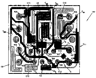
Figures 14-17 show an example circuit board layout for
implementing the compensation arrangement of Figure 10. Figures 15-17
respectively show the front, middle and back conductive layers 140, 142 and
144 of
the circuit board 132. Figure 14 is an overlay of the three conductive layers
140,
142 and 144. The circuit board 132 defines openings 301-308 that respectively
receive posts of the contact springs CS1-CS8 so that the contact springs CS i-
CS8 are
terminated to the board 132. The circuit board also defines openings 401-408
for
respectively receiving posts of the insulation displacement connector blades
IDC1-
IDC8 such that the insulation displacement connector blades IDC1-IDC8 are
terminated to the circuit board. Vias extend through the circuit board for
electrically
interconnecting the tracks between the layers 140, 142 and 144. For example,
vias
V6A, V6B and V6c interconnect the portions of the track T6 located at the
different
layers 140, 142 and 144. Also, vias V5A and V5B interconnect the portions of
the
track T5 located at the different layers 140, 142 and 144. Moreover, vias V4A
and
V48 interconnect the portions of the track T4 located at the different layers
140, 142
and 144. Additionally, via V3 interconnects the portions of the track T3
located at
the different layers 140, 142 and 144. The tracks Ti, T2, T7 and T8 are each
provided
on a single layer of the board 132. For example, tracks Ti and T2 are provided
at
layer 140 and tracks T7 and T8 are provided at layer 144.
13
CA 02649505 2008-10-10
WO 2007/120668 PCT/US2007/008847
Referring to Figures 14-16, the capacitive coupling Cl of the first
zone of compensation ZA1 is provided by opposing capacitor plates C15 and C13
respectively provided at layers 140 and 142. The capacitive coupling C2 of the
first
zone of compensation Ziti is provided by opposing capacitor plates C24 and C26
that
are respectively provided at the layers 140 and 142. The capacitive coupling
C3 of
the second compensation zone ZA2 is provided by opposing capacitor plates C34
and
C33 that are respectively provided at layers 140 and 142. The capacitive
coupling
C4 of the second compensation zone ZA2 is provided by opposing capacitor
plates
C45 and C46 that are respectively provided at layers 140 and 142. The
capacitive
coupling C5 of the third compensation zone ZA3 is provided by opposing
capacitor
plates C55A and C53A that are respectively provided at layers 140 and 142. The
capacitive coupling C5 is also provided by inter-digitated capacitor fingers
C558 and
C538 that are provided at layer 144. The capacitive coupling C6 of the second
compensation zone ZA3 is provided by opposing capacitor plates C66A and C64A
respectively provided at layers 140 and 142. The capacitive coupling C6 is
also
provided by inter-digitated capacitor fingers C66B and C603 provided at layer
144.
The capacitive coupling C7 of the first compensation zone ZBI is
provided by opposing capacitor plates C71 and C73 that are respectively
provided at
layers 140 and 142 of the circuit board. The capacitive coupling C8 of the
first
compensation zone Zgi is provided by opposing capacitor plates C82 and C86
that
are respectively provided at the layers 140 and 142 of the circuit board. The
capacitive coupling C9 of the second zone of compensation Z82 is provided by
inter-
digitated capacitor fingers C91 and C96 that are provided at layer 140 of the
circuit
board.
The capacitive coupling C10 of the first compensation zone Zci is
provided by opposing capacitor plates C105 and C108 that are respectively
provided
at layers 140 and 142 of the circuit board. The capacitive coupling C11 of the
second compensation zone ZC2 is provided by inter-digitated capacitor fingers
C114
and C118 that are provided at layer 144 of the circuit board.
The capacitive coupling C12 of the zone of compensation ZDI is
provided by inter-digitated capacitor fingers C122 and C125 provided at layer
140 of
the circuit board. The capacitive coupling C13 of the zone of compensation ZEI
is
provided by parallel capacitor fingers C138 and C136 provided at layer 144 of
the
circuit board. The capacitive coupling C14 is provided by inter-digitated
capacitor
14
CA 02649505 2008-10-10
WO 2007/120668 PCT/US2007/008847
fingers C145 and C146 that are provided at layer 144 of the circuit board. The
capacitive coupling C15 is provided by opposing capacitor plates C153 and C156
that are respectively provided at layers 140 and 142 of the circuit board. The
capacitive couplings C16 is provided by opposing capacitor plates Cl 64 and
C165
that are respectively provided at layers 140 and 142 of the circuit board.
Referring still to Figures 14-17, it is noted that the tracks T4 and T5
are routed away from one another for a majority of their lengths so as to
increase the
impedance of the tracks to address return loss. Similarly, tracks T3 and T6
are routed
away from one another for a majority of their lengths to also increase
impedance in
the tracks to address return loss. It is also noted that tracks T3-T6 also
preferably
have extended lengths to increase impedance for improving return loss
performance.
For example, referring to Figure 14, track T3 loops up and around as it
extends from
contact spring CS3 to its corresponding insulation displacement connector
blade
IDC3. Track T3 also includes a loop back 900 for further increasing the length
of the
track T3. Still referring to Figure 14, track T4 loops over, up and around as
it
extends from contact spring CS4 to its corresponding insulation displacement
connector blade IDC4. Referring further to Figure 14, track T5 loops up and
over as
it extends from contact spring CS5 to its corresponding insulation
displacement
connector blades IDC5. Additionally, track T5 has a loop back 902 for further
increasing the length of the track. Referring once again to Figure 14, track
T6
extends over up and around as it extends from contact spring CS6 to its
corresponding insulation displacement connector blade IDC6.
Referring still to Figure 14, the routing configuration of the tracks on
the circuit board are also adapted for positioning the capacitive couplings
C15 and
C16 relatively far from the center of the capacitive provided by the three
zones of
compensation ZAI-ZA3. For example, to provide this extra distance, loop
extension
portions 904 and 906 are provided with multiple loop backs for increasing the
spacings of the capacitive couplings C15, C16 from the center of the
capacitance
provided by the zones of compensation ZAI-ZA3.
The circuit board is also provided with structures adapted for
promoting manufacturing efficiency. For example, each set of opposing plate
capacitors has a first plate that is larger than the corresponding second
plate so that
portions of the first plate extend outwardly beyond the boundaries of the
second
plate. This facilitates manufacturing efficiency because the exact
registration
CA 02649505 2014-03-17
between the plates is not required. Additionally, some of the plates are
provided with stubs
910 that can be laser trimmed to exactly tune the capacitance so that the jack
satisfies the
relevant crosstalk requirements. The capacitance can also be tuned by using a
combination of
capacitor plates and parallel capacitor fingers at one zone of compensation.
Furthermore,
some of the tracks are provided with stubs 912 that can be used during design
of the circuit
board to manually vary the lengths of the tracks. In this way, the effect of
varying certain track
lengths can be empirically assessed.
The above specification provides examples of how certain inventive aspects may
be put
into practice. It will be appreciated that the inventive aspects can be
practiced in other ways
than those specifically shown and described herein without departing from the
scope of the
claims.
16