Note: Descriptions are shown in the official language in which they were submitted.
CA 02649545 2016-02-01
UNI-DIRECTIONAL LIGHT EMITTING DIODE DRIVE CIRCUIT IN
BI-DIRECTIONAL DIVIDED POWER IMPEDANCE
BACKGROUND OF THE INVENTION
(a) Field of the Invention
The uni-directional light emitting diode drive circuit in bi-directional
divided power
impedance is disclosed by that an AC power or a periodically alternated
polarity power
is used as the power source to supply to the resistive impedance components,
or
inductive impedance components, or capacitive impedance components in mutual
series connection, whereby the power source voltage is divided. Thereof, it is
characterized in that the said divided power is further rectified by a
rectifier device to
supply uni-directional DC power output to drive an uni-directional conducting
light
emitting diode, or to drive at least two rectifier devices which are
respectively parallel
connected across the two ends of the first impedance and the second impedance
while
the AC powers of the first impedance and second impedance are respectively
converted to DC power output through the said rectifier devices, thereby to
drive the
uni-directional conducting light emitting diodes individually.
(b) Description of the Prior Aft
The conventional light emitting diode drive circuit using AC or DC power
source is
usually series connected with current limit resistors as the impedance to
limit the
current to the light emitting diode, whereof the voltage drop of the series
connected
resistive impedance always result in waste of power and accumulation of heat
which
are the imperfections.
SUMMARY OF THE INVENTION
In accordance with an aspect of the present invention there is provided a uni-
directional light emitting diode drive circuit in bi-directional divided power
impedance, wherein a first impedance includes capacitive impedance components,
inductive impedance components, or resistive impedance components and a second
impedance includes capacitive impedance components, inductive impedance
components, or resistive impedance components; wherein, the first impedance
and the
1
CA 02649545 2016-02-01
second impedance are in series connection to receive the following: 1) AC
power with
a constant or variable voltage and a constant or variable frequency; or 2) AC
power
of bi-directional sinusoidal wave voltage or bi-directional square wave
voltage, or bi-
directional pulse wave voltage with constant or variable voltage and constant
or
variable frequency or period which is converted from a DC power source; or 3)
AC
power of bi-directional sinusoidal wave voltage or bi-directional square wave
voltage,
or bi-directional pulse wave voltage with constant or variable voltage and
constant or
variable frequency or period converted from the DC power which is further
rectified
from an AC power; a power source voltage input is divided by the first
impedance
and second impedance in series connection, wherein the divided power is
supplied to
a rectifier device which provides a DC power output through its DC output ends
to
drive a uni-directional conducting light emitting diode set which includes
light
emitting diodes to emit light; the first impedance, second impedance,
rectifier device
and uni-directional conducting light emitting diode set as well as the light
emitting
diode and various optional auxiliary circuit components are based on
application
needs, wherein the circuit components can be optionally installed or not
installed as
needed and the installed quantity may include one, wherein if more than one
circuit
component is selected in the application, the corresponding polarity
relationship of the
selected components shall be determined based on circuit function requirement
to
execute series connection, or parallel connection or series and parallel
connections,
wherein: a DC to AC Inverter (4000) including conventional electromechanical
components or solid state power components and related electronic circuit
components, wherein its input ends are optionally provided as needed to
receive input
from a constant or variable voltage DC power, or a DC power rectified from an
AC
power, while its output ends are optionally selected as needed to supply a bi-
directional
power of bi-directional sinusoidal wave, or bi-directional square wave or bi-
directional
pulsed wave AC power in a constant or variable voltage and constant or
variable
alternated polarity frequency or periods; the circuit operating functions are
the
following: the uni-directional light emitting diode drive circuit (U100) is
parallel
connected across the
2
CA 02649545 2016-02-01
output ends of the conventional DC to AC inverter; the input ends of the DC to
AC
inverter (4000) are optionally provided as needed to receive input from a
constant
orvariable voltage DC power, or a DC power rectified from an AC power; the
output
ends of the DC to AC inverter can be optionally selected as needed to provide
a bi-
directional power of hi-directional sinusoidal wave, or bi-directional square
wave, or
bi-directional pulse wave power in a constant or variable voltage and constant
or
variable alternated periods, which is used to control and drive the uni-
directional light
emitting diode drive circuit; in addition, the uni-directional light emitting
diode drive
circuit can be controlled and driven by means of modulating the output power
from
the DC to AC inverter, as well as by executing power modulations to the power
outputted such as pulse width modulation, or conductive current phase angle
control,
or impedance modulation.
BRIEF DESCRIPTON OF THE DRAWINGS
Fig. 1 is the schematic block diagram of the uni-directional light emitting
diode
drive circuit in bi-directional divided power impedance.
Fig. 2 is the circuit example schematic diagram of the invention.
Fig. 3 is a circuit example schematic diagram illustrating that the uni-
directional conducting light emitting diode set in the circuit of Fig. 2 is
further installed
with a zener diode.
Fig. 4 is a circuit example schematic diagram illustrating that a
charge/discharge device is parallel connected across the two ends of the
2a
CA 02649545 2009-01-13
light emitting diode and the current limit resistor in series connection in
the circuit of Fig. 3.
Fig. 5 is a circuit example schematic diagram illustrating that a
charge/discharge device is parallel connected with the light emitting diode
in the circuit of Fig. 3.
Fig. 6 is a circuit example schematic block diagram of the invention
which is series connected to the power modulator of series connection
type.
Fig. 7 is a circuit example schematic block diagram of the invention
which is parallel connected to the power modulator of parallel connection
type.
Fig. 8 is a circuit example schematic block diagram illustrating that
the invention is series connected with a periodically alternated power
modulator of series connection type which is driven by the output power
of the DC to AC inverter.
Fig. 9 is a circuit example schematic block diagram illustrating that
the invention is parallel connected with a periodically alternated power
modulator of parallel connection type which is driven by the output power
of the DC to AC inverter.
Fig. 10 is a circuit example schematic block diagram of the invention
driven by the DC to AC converter output power.
Fig. 11 is a circuit example schematic block diagram of the invention
which is series connected with impedance components.
Fig. 12 is a circuit example schematic block diagram of the invention
illustrating that the impedance components in series connection execute
series connection, or parallel connection, or series and parallel connection
by means of the switching device.
Fig. 13 is a circuit example schematic diagram of the invention
illustrating that the inductive impedance component of the second
impedance is replaced by the self-coupled voltage change power supply
3
CA 02649545 2009-01-13
side winding of the self-coupled transformer thereby to constitute a
voltage rise.
Fig. 14 is a circuit example schematic diagram of the invention
illustrating that the inductive impedance component of the second
impedance is replaced by the self-coupled voltage change power supply
side winding of the self-coupled transformer thereby to constitute a
voltage drop.
Fig. 15 is a circuit example schematic diagram of the invention
illustrating that the inductive impedance component of the second
impedance is replaced by the primary side winding of the separating type
transformer with separating type voltage change winding.
Fig. 16 is a circuit example schematic diagram of the invention
illustrating that the self-coupled voltage change power supply side
winding of the self-coupled transformer is in parallel resonance with the
parallel connected capacitive impedance component to constitute a
voltage rise.
Fig. 17 is a circuit example schematic diagram of the invention
illustrating that the self-coupled voltage change power supply side
winding of the self-coupled transformer is in parallel resonance with the
parallel connected capacitive impedance component to constitute a
voltage drop.
Fig. 18 is a circuit example schematic diagram of the invention
illustrating that the primary side winding of the separating type
transformer with separating type voltage change winding is parallel
connected with a capacitive impedance component to appear a parallel
resonance status.
DESCRIPTION OF MAIN COMPONENT SYMBOLS
BR101: Rectifier device
C100, C102, C200: Capacitor
4
CA 02649545 2009-01-13
CR201: Diode
ESD101: Charge/discharge device
1103, 1200: Inductive impedance component
IT200: Separating type transformer
L100: Uni-directional conducting light emitting diode set
LED101: Light emitting diode
R101, R102: Discharge resistor
R103: Current limit resistor
ST200: Self-coupled transformer
U100: Uni-directional light emitting diode (LED) drive circuit
WO: Self-coupled voltage change winding
Wl: Primary side winding
W2: Secondary side winding
Z101: First impedance
Z102: Second impedance
ZD101: Zener diode
300: Bi-directional power modulator of series connection type
360: DC power modulator of series connection type
400: Bi-directional power modulator of parallel connection type
460: DC power modulator of parallel connection type
500: Impedance component
600: Switching device
4000: DC to AC Inverter
DETAILED DESCRIPTION OF THE PREFERRED EMOBODIMENTS
The uni-directional light emitting diode drive circuit in bi-directional
divided power impedance is disclosed by that the first impedance is
constituted by at least one capacitive impedance component, inductive
impedance component, or resistive component and the second impedance
is constituted by at least one capacitive impedance component, inductive
5
CA 02649545 2009-01-13
impedance component, or resistive impedance component. Thereof the
first impedance and the second impedance are in series connection,
whereof at least one rectifier device is installed, and the input ends of the
said rectifier device is provided to receive the divided power across the
two ends of the first impedance or the second impedance and the DC
power output from the said rectifier device is used to drive at least one
uni-directional conducting light emitting diode;
The two ends of the first impedance and the second impedance in
series connection are provided to receive:
(1) The AC power with a constant or variable voltage and a constant
or variable frequency; or
(2) The AC power of bi-directional sinusoidal wave voltage or
bi-directional square wave voltage, or bi-directional pulse wave
voltage with constant or variable voltage and constant or variable
frequency or period which is converted from a DC power source;
or
(3) The AC power of bi-directional sinusoidal wave voltage or
bi-directional square wave voltage, or bi-directional pulse wave
voltage with constant or variable voltage and constant or variable
frequency or period converted from the DC power which is further
rectified from an AC power;
The bi-directional divided power of the first impedance or the second
impedance is rectified by the rectifier device to drive at least one
uni-directional conducting light emitting diode or is driven by at least two
rectifier devices which are respectively parallel connected across the two
ends of the first and second impedances for the rectifier devices to
respectively receive the AC power of the first and second impedances and
rectify as DC power output to drive the individual uni-directional
conducting light emitting diodes.
Fig. 1 is the schematic block diagram of the uni-directional light
6
CA 02649545 2009-01-13
emitting diode drive circuit in,bi-directional divided power impedance, in
which the circuit function is operated through the uni-directional light
emitting diode drive circuit (U100) as shown in Fig. 1, whereof it is
comprised of that:
-- A first impedance (Z101) is comprised of that:
(1) A first impedance (Z101) is comprised of capacitive impedance
components, or inductive impedance components or resistive impedance
components, whereof it can be optionally installed as needed one kind or
more than one kind and one or more than one impedance components, or
can be optionally installed as needed by two or more than two kinds of
impedance components, whereof each kind of impedance components can
be respectively to be one or more than one in series connection, or parallel
connection or series and parallel connection; or
(2) The first impedance (Z101) is constituted by at least one
capacitive impedance component and at least one inductive impedance
component in mutually series connection, whereof their inherent series
resonance frequency is the same as the frequency of bi-directional power
from power source such as the AC power, or the alternated polarity period
of the constant or variable periodically alternated polarity power
converted from a DC power, thereby to appear in a series resonance
impedance status; or
(3) The first impedance (Z101) is constituted by at least one
capacitive impedance component and at least one inductive impedance
component in mutual parallel connection, whereof their inherent parallel
resonance frequency after parallel connection is the same as frequency of
the bi-directional power from power source such as the AC power, or the
alternated polarity period of the constant or variable periodically
alternated polarity power converted from a DC power, thereby to appear a
parallel resonance impedance status;
-- A second impedance (Z102) is comprised of that:
7
CA 02649545 2009-01-13
(1) A second impedance (Z102) is comprised of capacitive
impedance components, or inductive impedance components or resistive
impedance components, whereof it can be optionally installed as needed
one kind or more than one kind and one or more than one impedance
components, or can be optionally installed as needed by two or more than
two kinds of impedance components, whereof each kind of impedance
components can be respectively to be one or more than one in series
connection, or parallel connection or series and parallel connection; or
(2) The second impedance (Z102) is constituted by at least one
capacitive impedance component and at least one inductive impedance
component in mutually series connection, whereof their inherent series
resonance frequency is the same as the frequency of bi-directional power
from power source such as the AC power, or the alternated polarity period
of the constant or variable periodically alternated polarity power
converted from a DC power, thereby to appear in a series resonance
impedance status; or
(3) The second impedance (Z102) is constituted by at least one
capacitive impedance component and at least one inductive impedance
component in mutual parallel connection, whereof their inherent parallel
resonance frequency after parallel connection is the same as frequency of
the bi-directional power from power source such as the AC power, or the
alternated polarity period of the constant or variable periodically
alternated polarity power converted from a DC power, thereby to appear a
parallel resonance impedance status;
-- At least one first impedance (Z101) and at least one second
impedance (Z102) are mutually series connected, whereof the two ends of
the first impedance (Z101) and the second impedance (Z102) in series
connection are provided for:
(1) The AC power with a constant or variable voltage and a constant
or variable frequency; or
8
CA 02649545 2009-01-13
(2) The AC power of bi-directional sinusoidal wave voltage or
bi-directional square wave voltage, or bi-directional pulse wave
voltage with constant or variable voltage and constant or variable
frequency or period which is converted from a DC power source;
or
(3) The AC power of bi-directional sinusoidal wave voltage or
bi-directional square wave voltage, or bi-directional pulse wave
voltage with constant or variable voltage and constant or variable
frequency or period converted from the DC power which is further
rectified from an AC power;
The divided power is formed at the two ends of the first impedance
(Z101) and the two ends of the second impedance (Z102) trough power
input, whereof the divided power is provided to the AC input ends of the
rectifier device (BR101);
-- A rectifier device (BR101): It is parallel connected across the two
ends of the first impedance (Z101) or the second impedance (Z102), or
respectively parallel connected across two ends of the first impedance
(Z101) and the second impedance (Z102) simultaneously, thereby the
divided power across the two ends of the first impedance (Z101) or the
second impedance (Z102) is rectified to a DC power which is used to
drive the uni-directional conducting light emitting diode set (L100);
The rectifier device can be constituted by a bridge type rectifier device
or by a half-wave rectifier device, whereof the number of rectifier device
(BR101) can be one or more than one;
-- An uni-directional conducting light emitting diode set (L100): The
uni-directional conducting light emitting diode set (L100) is constituted
by a forward current polarity light emitting diode, or two or more than
two forward current polarity light emitting diodes in series connection or
parallel connection, or three or more than three forward current polarity
light emitting diodes in series connection, parallel connection or series
9
CA 02649545 2009-01-13
and parallel connection; ,
The uni-directional conducting light emitting diode set (L100) can be
selected as needed to be installed one set or more than one sets to be
driven by DC power output from the rectifier device (BR101);
One or more than one first impedance (Z101), second impedance
(Z102), uni-directional conducting light emitting diode set (L100) and
rectifier device (BR101) in the uni-directional light emitting diode drive
circuit (U100) can be optionally installed as needed.
The divided power produced by the first impedance or the second
impedance is rectified by a rectifier device to DC power and is used to
drive at least one uni-directional conducting light emitting diode, or the
AC powers of the first impedance and the second impedance are
respectively rectified by two rectifier devices which are respectively
parallel connected across the two ends of the first impedance and the
second impedance to DC powers and are used to drive the individual
uni-directional conducting light emitting diodes.
For convenience of description, the components listed in the circuit
examples of the following exemplary embodiments are selected as in the
following:
(1) A first impedance (Z101), a second impedance (Z102), a
rectifier device (BR101) and an uni-directional conducting light emitting
diode set (L100) are installed in the embodied examples. Nonetheless, the
selected quantities are not limited in actual applications;
(2) A
capacitive impedance of the capacitor is selected to represent
the impedance component, whereby to constitute the first impedance
(Z101) and the second impedance (Z102) in the embodied examples. In
actual applications, the impedance components can be optionally selected
as needed to be constituted by various capacitive impedance components,
inductive impedance components or resistive impedance components,
wherein it is described in the following.
CA 02649545 2009-01-13
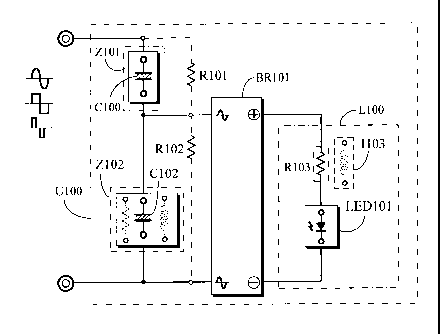
Fig. 2 is the circuit example schematic diagram of the invention which
is mainly constituted by the following:
-- A first impedance (Z101): it is constituted by at least one capacitive
impedance component, especially by the capacitor (C100), whereof the
number of the first impedance can be one or more than one;
-- A second impedance (Z102): it is constituted by at least one
capacitive impedance component, especially by the capacitor (C102),
whereof the number of the second impedance can be one or more than
one;
-- At least one first impedance (Z101) and at least one second
impedance (Z102) are in series connection, whereof the two ends of them
after series connection are provided for receiving:
(1) The AC power with a constant or variable voltage and a constant
or variable frequency; or
(2) The AC power of bi-directional sinusoidal wave voltage or
bi-directional square wave voltage, or bi-directional pulse wave
voltage with constant or variable voltage and constant or variable
frequency or period which is converted from a DC power source;
or
(3) The AC power of bi-directional sinusoidal wave voltage or
bi-directional square wave voltage, or bi-directional pulse wave
voltage with constant or variable voltage and constant or variable
frequency or period converted from the DC power which is
further rectified from an AC power;
-- A rectifier device (BR101): at least one rectifier device (BR101) is
installed to receive the divided power from the two ends of the first
impedance (Z101) or the second impedance (Z102) , or two or more than
two rectifier devices (BR101) are respectively installed to receive the
divided power from the two ends of the first impedance (Z101) or the
second impedance (Z102) thereby the divided power across the two ends
11
CA 02649545 2009-01-13
of the first impedance (Z101) or the second impedance (Z102) is rectified
to DC power to drive the uni-directional conducting light emitting diode
set (L100);
The rectifier device can be constituted by a bridge type rectifier device
or by a half-wave rectifier device, whereof the number of rectifier device
(BR101) can be one or more than one;
-- An uni-directional conducting light emitting diode set (L100): The
uni-directional conducting light emitting diode set (L100) is constituted
by a forward current polarity light emitting diode (LED101), or two or
more than two forward current polarity light emitting diodes (LED101) in
series connection or parallel connection, or three or more than three
forward current polarity light emitting diodes (LED101) in series
connection, parallel connection or series and parallel connection; one or
more than one set of the uni-directional conducting light emitting diode
set (L100) can be optionally installed as needed to be driven by the DC
power output from the rectifier device (BR101);
-- The AC input ends of the rectifier device (BR101) are provided to
receive the divided power across the two ends of the capacitor (C102)
which constitute the second impedance (Z102), whereby the
uni-directional conducting light emitting diode set (L100) is driven by the
DC power rectfied by the said rectifier unit (BR101), and the first
impedance (Z101) is used to limit its current, whereof in case that the
capacitor (C100) is used as the first impedance component, its output
current is limited by the capacitive impedance;
-- A discharge resistor (R101): It is an optionally installed component
as needed to be parallel connected across the two ends of the capacitor
(C100) which constitutes the first impendence (Z101) to release the
residual charge of capacitor (C100);
-- A discharge resistor (R102): It is an optionally installed component
as needed to be parallel connected across the two ends of the capacitor
12
CA 02649545 2009-01-13
(C102) which constitutes the ,second impendence (Z102) to release the
residual charge of capacitor (C102);
--A current limit resistor (R103): It is an optionally installed
component as needed to be individually series connected with each of
light emitting diodes (LED101) which constitute the uni-directional
conducting light emitting diode set (L100), whereby to limit the current
passing through the light emitting diode (LED101); whereof the current
limit resistor (R103) can also be replaced by an inductive impedance
component (1103).
The uni-directional light emitting diode drive circuit (U100) is
constituted by the first impedance (Z101), the second impedance (Z102),
the rectifier device (BR101) and the uni-directional conducting light
emitting diode set (L100) according to above said circuit structure;
In addition, the uni-directional conducting light emitting diode set
(L100) in the uni-directional light emitting diode drive circuit (U100) of
the uni-directional light emitting diode drive circuit in bi-directional
divided power impedance is through the divided power distribution effect
by the parallel connection between the rectifier device (BR101) and the
second impedance (Z102) to reduce the voltage variation rate across the
two ends of uni-directional conducting light emitting diode set (L100)
corresponding to the power source of voltage variation.
The light emitting diode (LED101) which constitutes the
uni-directional conducting light emitting diode set (L100) in the
uni-directional light emitting diode drive circuit (U100) of the
uni-directional light emitting diode drive circuit in bi-directional divided
power impedance includes the following selections:
The uni-directional conducting light emitting diode set (L100) is
constituted by a forward current polarity light emitting diode (LED101),
or two or more than two forward current polarity light emitting diodes
(LED101) in series connection or parallel connection, or three or more
13
CA 02649545 2009-01-13
than three forward current polarity light emitting diodes (LED101) in
series connection, parallel connection or series and parallel connection,
whereof one or more than one set of the uni-directional conducting light
emitting diode set (L100) can be optionally installed as needed;
In addition, to protect the light emitting diode and to avoid the light
emitting diode (LED101) being damaged or reduced working life by
abnormal voltage, a zener diode can be further parallel connected across
the two ends of the light emitting diode (LED101) of the uni-directional
conducting light emitting diode set (L100) in the uni-directional light
emitting diode drive circuit (U100) of the uni-directional light emitting
diode drive circuit in bi-directional divided power impedance, or the zener
diode can be first series connected with at least one diode to produce
zener voltage function, then parallel connected across the two ends of the
light emitting diode (LED101);
Fig. 3 is a circuit example schematic diagram illustrating that the
uni-directional conducting light emitting diode set in the circuit of Fig. 2
is further installed with a zener diode, whereof it is constituted by the
following:
-- A zener diode (ZD101) is parallel connected across the two ends of
the light emitting diode (LED101) of the uni-directional conducting light
emitting diode set (L100) in the uni-directional light emitting diode drive
circuit (U100), whereof their polarity relationship is that the zener voltage
of the zener diode (ZD101) is used to limit the working voltage across the
two ends of the light emitting diode (LED101);
-- A zener diode (ZD101) is parallel connected across the two ends of
the light emitting diode (LED101) of the uni-directional conducting light
emitting diode set (L100) in the uni-directional light emitting diode drive
circuit (U100), whereof the said zener diode (ZD101) can be optionally
series connected with a diode (CR201) as needed to produce the zener
voltage effect together, whereby the advantages are 1) the zener diode
14
CA 02649545 2009-01-13
(ZD101) can be protected from abnormal reverse voltage; 2) both diode
(CR201) and zener diode (ZD101) have temperature compensation effect.
To promote the lighting stability of the light source produced by the
light emitting diode in the uni-directional light emitting diode drive circuit
(U100) of the uni-directional light emitting diode drive circuit in
bi-directional divided power impedance, the light emitting diode (LED101)
can be further installed with a charge/discharge device (ESD101), whereof
random power charging or discharging can be provided by the
charge/discharge device (ESD101) to stabilize the lighting stability of the
light emitting diode (LED101), whereby to reduce its lighting pulsation,
or in case of power supply off, reserved power can be supplied by the
charge/discharge device (ESD101) to drive the light emitting diode
(LED101) to emit light continuously;
As shown in Fig. 4, which is a circuit example schematic diagram
illustrating that a charge/discharge device is parallel connected across the
two ends of the light emitting diode and the current limit resistor in series
connection in the circuit of Fig. 3.
As shown in Fig. 5, which is a circuit example schematic diagram
illustrating that a charge/discharge device is parallel connected across the
two ends of the light emitting diode in the circuit of Fig. 3.
Fig. 4 and Fig. 5 are comprised of that:
-- The uni-directional conducting light emitting diode set (L100) can
be further installed with a charge/discharge device (ESD101) including to
be parallel connected across the two ends of the light emitting diode
(LED101) and the current limit resistor (R103) in series connection as
shown in Fig. 4, or across the two ends of the light emitting diode
(LED101) as shown in Fig. 5 according to polarities, whereof random
power charging or discharging can be provided by the charge/discharge
device (ESD101) to stabilize the lighting stability of the light emitting
diode (LED101), whereby to reduce its lighting pulsation, or in case of
CA 02649545 2009-01-13
power supply off, reserved power can be supplied by the charge/discharge
device (ESD101) to drive the light emitting diode (LED101) to emit light
continuously.
-- The aforesaid charge/discharge device (ESD101) can be constituted
by the conventional charging and discharging batteries, or
super-capacitors or capacitors, etc.
The first impedance (Z101), second impedance (Z102), rectifier
device (BR101) and uni-directional conducting light emitting diode set
(L100) as well as the light emitting diode (LED101) and various aforesaid
optional auxiliary circuit components as shown in the circuit examples of
Figs. 1-5 are based on application needs, whereof they can be optionally
installed or not installed as needed and the installation quantity include
constitution by one, wherein if more than one are selected in the
application, the corresponding polarity relationship shall be determined
based on circuit function requirement to execute series connection, or
parallel connection or series and parallel connections; thereof it is
constituted as the following:
1. The first impedance (Z101) can be constituted by one or by more
than one in series connection or parallel connection or series and parallel
connection, whereof in multiple installations, each first impedance can be
constituted by the same kind of capacitive impedance components,
inductive impedance components, or resistive impedance components, or
other different kinds of impedance components, in which their impedance
values can be the same or different;
2. The second impedance (Z102) can be constituted by one or by
more than one in series connection or parallel connection or series and
parallel connection, whereof in multiple installation, each second
impedance can be constituted by the same kind of capacitive impedance
components, inductive impedance components, or resistive impedance
components, or other different kinds of impedance components, in which
16
CA 02649545 2009-01-13
their impedance values can be the same or different;
3. The light emitting diode (LED101) can be constituted by one light
emitting diode, or by more than one light emitting diodes in series
connection, parallel connection or series and parallel connection;
4. In the uni-directional light emitting diode drive circuit (U100):
(1) The uni-directional conducting light emitting diode set
(L100) can be optionally selected to be installed by one set or can be
selected to be installed by more than one sets in series connection, parallel
connection or series and parallel connection, whereof if one or more than
one sets are installed, it can be jointly driven by the divided power of the
same second impedance (Z102) through its matched rectifier device
(BR101), or it can be individually driven by the divided power of multiple
second impedances (Z102) in series or parallel connection, whereof each
of the multiple second impedances (Z102) is installed with a rectifier
device (BR101) individually to drive its corresponding matched
uni-directional conducting light emitting diode set (L100) individually;
(2) If a charge/discharge device (ESD101) is installed in the
uni-directional light emitting diode drive circuit (U100), then the light
emitting diode (LED101) of the uni-directional conducting light emitting
diode set (L100) is driven by DC power to emit light continuously;
If the charge/discharge device (ESD101) is not installed, then
current conduction to light emitting diode (LED101) is intermittent,
whereby referring to the input voltage wave shape and duty cycle of
current conduction, the light emitting forward current and the peak of
light emitting forward voltage of each light emitting diode in the
uni-directional conducting light emitting diode set (L100) can be
correspondingly selected for the light emitting diode (LED101), whereof
the selections include the following:
1) The light emitting peak of forward voltage is lower than the
rated forward voltage of light emitting diode (LED101); or
17
CA 02649545 2009-01-13
2) The rated forward voltage of light emitting diode (LED101)
is selected to be the light emitting peak of forward voltage; or
3) If current conduction to light emitting diode (LED101) is
intermittent, the peak of light emitting forward voltage can be
correspondingly selected based on the duty cycle of current conduction as
long as the principle of that the peak of light emitting forward voltage
does not damage the light emitting diode (LED101) is followed;
Based on the value and wave shape of the aforesaid light emitting
forward voltage, the corresponding current value and wave shape from the
forward voltage vs. forward current ratio are produced; however the peak
of light emitting forward current shall follow the principle not to damage
the light emitting diode (LED101);
The luminosity or the stepped or step-less luminosity modulation
of the forward current vs. relative luminosity can be controlled based on
the aforesaid value and wave shape of forward current;
5. The discharge resistor (R101) can be optionally installed as
needed to be constituted by one resistor, or by more than one resistors in
series connection or parallel connection or series and parallel connection;
6. The discharge resistor (R102) can be optionally installed as
needed to be constituted by one resistor, or by more than one resistors in
series connection or parallel connection or series and parallel connection;
7. The current limit resistor (R103) can be optionally installed as
needed to be constituted by one resistor, or by more than one resistors in
series connection or parallel connection or series and parallel connection;
8. The inductive impedance component (1103) can be constituted by
one impedance component, or by more than one impedance components
in series connection or parallel connection or series and parallel
connection, whereof the said devices can be optionally installed as
needed;
9. The zener diode (ZD101) can be constituted by one zener diode,
18
CA 02649545 2009-01-13
or by more than one zener diodes in series connection or parallel
connection or series and parallel connection, whereof the said devices can
be optionally installed as needed;
10. The diode (CR201) can be constituted by one diode, or by more
than one diodes in series connection or parallel connection or series and
parallel connection, whereof the said devices can be optionally installed as
needed;
11. The charge/discharge device (ESD101) can be constituted by one
or by more than one in series connection or parallel connection or series
and parallel connection, whereof the said devices can be optionally
installed as needed;
In the application of the uni-directional light emitting diode drive
circuit (U100) of the uni-directional light emitting diode drive circuit in
bi-directional divided power impedance, the following different types of
bi-directional power can be provided for inputs, whereof the bi-directional
power includes that:
(1) The AC power with a constant or variable voltage and a constant
or variable frequency; or
(2) The AC power of bi-directional sinusoidal wave voltage or
bi-directional square wave voltage, or bi-directional pulse wave
voltage with constant or variable voltage and constant or variable
frequency or period which is converted from a DC power source;
or
(3) The AC power of bi-directional sinusoidal wave voltage or
bi-directional square wave voltage, or bi-directional pulse wave
voltage with constant or variable voltage and constant or variable
frequency or period converted from the DC power which is further
rectified from an AC power;
In addition, the following active modulating circuit devices can be
further optionally combined as needed, whereof the applied circuits are
19
CA 02649545 2009-01-13
,
the following:
1. Fig. 6 is a circuit example schematic block diagram of the
invention which is series connected to the power modulator of series
connection type, whereof the power modulator of series connection type is
constituted by the following:
-- A bi-directional power modulator of series connection type
(300): It is constituted by the conventional electromechanical components
or solid state power components and related electronic circuit components
to modulate the bi-directional power output.
-- A DC power modulator of series connection type (360): It is
constituted by the conventional electromechanical components or solid
state power components and related electronic circuit components to
modulate the DC power for voltage stabilization, or DC pulsed power
output.
The circuit operating functions are the following:
(1) The bi-
directional power modulator of series connection
type (300) can be optionally installed as needed to be series connected
with the uni-directional light emitting diode drive circuit (U100) to
receive the bi-directional power from power source, whereby the
bi-directional power is modulated by the bi-directional power modulator
of series connection type (300) to execute power modulations such as
pulse width modulation or current conduction phase angle control, or
impedance modulation, etc. to drive the uni-directional light emitting
diode drive circuit (U100); or
(2) The bi-directional power modulator of series connection
type (300) can be optionally installed as needed to be series connected
between the second impedance (Z102) and the AC input ends of the
rectifier device (BR101) whereby the bi-directional divided power from
the two ends of the second impedance (Z102) is modulated by the
bi-directional power modulator of series connection type (300) to execute
CA 02649545 2009-01-13
power modulations such as pulse width modulation or current conduction
phase angle control, or impedance modulation, etc. to drive the
uni-directional conducting light emitting diode set (L100) through the
rectifier device (BR101); or
(3) The DC power modulator of series connection type (360)
can be optionally installed as needed to be series connected between the
DC output ends of the rectifier device (BR101) and the uni-directional
conducting light emitting diode set (L100), whereby DC power from the
rectifier device (BR101) is modulated by the DC power modulator of
series connection type (360) to execute power modulations such as pulse
width modulation or current conduction phase angle control, or
impedance modulation, etc. to drive the uni-directional conducting light
emitting diode set (L100);
2. Fig. 7
is a circuit example schematic block diagram of the
invention which is parallel connected to a power modulator of parallel
connection type, whereof the power modulator of parallel connection type
is constituted by the following:
-- A bi-directional power modulator of parallel connection type
(400): It is constituted by the conventional electromechanical components
or solid state power components and related electronic circuit components
to modulate the bi-directional power output;
-- A DC power modulator of parallel connection type (460): It is
constituted by the conventional electromechanical components or solid
state power components and related electronic circuit components to
modulate the DC power for voltage stabilization, or DC pulsed power
output;
The circuit operating functions are the following:
(1) The bi-
directional power modulator of parallel connection
type (400) can be optionally installed as needed, whereof its output ends
are for parallel connection with the uni-directional light emitting diode
21
CA 02649545 2009-01-13
drive circuit (U100), while its input ends are provided for receiving the
bi-directional power from the power source, whereby the bi-directional
power is modulated by the bi-directional power modulator of parallel
connection (400) to execute power modulations such as pulse width
modulation or current conduction phase angle control, or impedance
modulation, etc. to drive the uni-directional light emitting diode drive
circuit (U100); or
(2) The bi-directional power modulator of parallel connection
type (400) can be optionally installed as needed, whereof its output ends
are parallel connected with the bi-directional power input ends of the
rectifier device (BR101) while its input ends are parallel connected across
the two ends of the second impedance (Z102), whereby the bi-directional
divided power across the two ends of the second impedance (Z102) is
modulated by the bi-directional power modulator of parallel connection
type (400) to execute power modulations such as pulse width modulation
or current conduction phase angle control, or impedance modulation, etc.
to drive the uni-directional conducting light emitting diode set (L100) by
the DC power which is rectified by the rectifier device (BR101); or
(3) The DC power modulator of parallel connection type (460)
can be optionally installed as needed, whereof its output ends are parallel
connected with the uni-directional conducting light emitting diode set
(L100), while its input ends are parallel connected with the DC output
ends of the rectifier device (BR101), whereby the DC power of the
rectifier device (BR101) is modulated by the DC power modulator of
parallel connection type (460) to execute power modulations such as pulse
width modulation or current conduction phase angle control, or
impedance modulation, etc. to drive the uni-directional conducting light
emitting diode set (L100);
3. Fig. 8 is a circuit example schematic block diagram illustrating
that the invention is series connected with a power modulator of series
22
CA 02649545 2009-01-13
connection type which is driven by the output power of the DC to AC
inverter, whereof the constitutions of the DC to AC inverter and the power
modulator of series connection type include the following:
-- A DC to AC Inverter (4000): it is constituted by the
conventional electromechanical components or solid state power
components and related electronic circuit components, whereof its input
ends are optionally provided as needed to receive input from a constant or
variable voltage DC power, or a DC power rectified from an AC power,
while its output ends are optionally selected as needed to supply a
bi-directional power of bi-directional sinusoidal wave, or bi-directional
square wave or bi-directional pulsed wave AC power in a constant or
variable voltage and constant or variable alternated polarity frequency or
periods;
-- A bi-directional power modulator of series connection type
(300): It is constituted by the conventional electromechanical components
or solid state power components and related electronic circuit components
to modulate the bi-directional power output.
-- A DC power modulator of series connection type (360): It is
constituted by the conventional electromechanical components or solid
state power components and related electronic circuit components to
modulate the DC power for voltage stabilization, or DC pulsed power
output.
The circuit operating functions are described in the following:
(1) A bi-directional power modulator of series connection type
(300) can be optionally installed as needed to series connected with the
uni-directional light emitting diode drive circuit (U100). After the two are
in series connection, they are parallel connected with the output ends of
the DC to AC inverter (4000), and the output ends of the DC to AC
inverter can be optionally selected as needed to provide a bi-directional
power of a bi-directional sinusoidal wave ,square wave or pulse wave
23
CA 02649545 2009-01-13
power output at a constant or, variable voltage and constant or variable
alternated polarity frequency or periods, and the bi-directional power
output of the DC to AC inverter (4000) is modulated by the bi-directional
power modulator of series connection type (300) to execute power
modulations such as pulse width modulation or current conduction phase
angle control, or impedance modulation, etc. to drive the uni-directional
light emitting diode drive circuit (U100); or
(2) The bi-directional power modulator of series connection
type (300) can be optionally installed as needed to be series connected
between the second impedance (Z102) and the AC input ends of the
rectifier device (BR101) whereby the bi-directional divided power across
the two ends of the second impedance (Z102) is modulated by the
bi-directional power modulator of series connection type (300) to execute
power modulations such as pulse width modulation or current conduction
phase angle control, or impedance modulation, etc. to drive the
uni-directional conducting light emitting diode set (L100) through the
rectifier device (BR101); or
(3) The DC power modulator of series connection type (360)
can be optionally installed as needed to be series connected between the
DC output ends of the rectifier device (BR101) and the uni-directional
conducting light emitting diode set (L100), whereby DC power from the
rectifier device (BR101) is modulated by the DC power modulator of
series connection type (360) to execute power modulations such as pulse
width modulation or current conduction phase angle control, or
impedance modulation, etc. to drive the uni-directional conducting light
emitting diode set (L100);
4. Fig. 9 is a circuit example schematic block diagram illustrating
that the invention is parallel connected with a power modulator of parallel
connection type which is driven by the output power of the DC to AC
inverter, whereof the constitutions of the DC to AC inverter and the power
24
CA 02649545 2009-01-13
modulator of parallel connection type include the following:
-- A DC to AC Inverter (4000): it is constituted by the
conventional electromechanical components or solid state power
components and related electronic circuit components, whereof its input
ends are optionally provided as needed to receive input from a constant or
variable voltage DC power, or a DC power rectified from an AC power,
while its output ends are optionally selected as needed to supply a
bi-directional power of bi-directional sinusoidal wave, or bi-directional
square wave or bi-directional pulsed wave AC power in a constant or
variable voltage and constant or variable alternated polarity frequency or
periods;
-- A bi-directional power modulator of parallel connection type
(400): It is constituted by the conventional electromechanical components
or solid state power components and related electronic circuit components
to modulate the bi-directional power output;
-- A DC power modulator of parallel connection type (460): It is
constituted by the conventional electromechanical components or solid
state power components and related electronic circuit components to
modulate the DC power for voltage stabilization, or DC pulsed power
output.
The circuit operating functions are described in the following:
(1) A bi-directional power modulator of parallel connection
type (400) can be optionally installed as needed, whereof its output ends
are parallel connected with the input ends of the uni-directional light
emitting diode drive circuit (U100) and its input ends are provided to
receive the bi-directional power output from the DC to AC inverter (4000),
whereby the bi-directional power output of the DC to AC invert (4000) is
modulated by the bi-directional power modulator of parallel connection
type (400) to execute power modulations such as pulse width modulation
or current conduction phase angle control, or impedance modulation, etc.
CA 02649545 2009-01-13
to drive the uni-directional light emitting diode drive circuit (U100); or
(2) The bi-directional power modulator of parallel connection
type (400) can be optionally installed as needed, whereof its output ends
are parallel connected with the AC input ends of the rectifier device
(BR101) while its input ends are parallel connected with the second
impedance (Z102), whereby the bi-directional divided power across the
two ends of the second impedance (Z102) is modulated by the
bi-directional power modulator of parallel connection type (400) to
execute power modulations such as pulse width modulation or current
conduction phase angle control, or impedance modulation, etc. to drive
the uni-directional conducting light emitting diode set (L100) through the
rectifier device (BR101); or
(3) The DC power modulator of parallel connection type (460)
can be optionally installed as needed, whereof its output ends are parallel
connected with the uni-directional conducting light emitting diode set
(L100), while its input ends are parallel connected with the DC output
ends of the rectifier device (BR101), whereby the DC power of the
rectifier device (BR101) is modulated by the DC power modulator of
parallel connection type (460) to execute power modulations such as pulse
width modulation or current conduction phase angle control, or
impedance modulation, etc. to drive the uni-directional conducting light
emitting diode set (L100);
5. Fig. 10 is a circuit example schematic block diagram of the
invention driven by a DC to AC converter output power; it is mainly
comprised of that:
-- A DC to AC Inverter (4000): it is constituted by the
conventional electromechanical components or solid state power
components and related electronic circuit components, whereof its input
ends are optionally provided as needed to receive input from a constant or
variable voltage DC power, or a DC power rectified from an AC power,
26
CA 02649545 2009-01-13
while its output ends are optionally selected as needed to supply a
bi-directional power of bi-directional sinusoidal wave, or bi-directional
square wave or bi-directional pulsed wave AC power in a constant or
variable voltage and constant or variable alternated polarity frequency or
periods;
The circuit operating functions are the following:
-- The uni-directional light emitting diode drive circuit (U100) is
parallel connected across the output ends of the conventional DC to AC
inverter (4000); the input ends of the DC to AC inverter (4000) are
optionally provided as needed to receive input from a constant or variable
voltage DC power, or a DC power rectified from an AC power.
-- The output ends of the DC to AC inverter (4000) can be optionally
selected as needed to provide a bi-directional power of bi-directional
sinusoidal wave, or bi-directional square wave, or bi-directional pulse
wave power in a constant or variable voltage and constant or variable
alternated periods, which is used to control and drive the uni-directional
light emitting diode drive circuit (U100).
-- In addition, the uni-directional light emitting diode drive circuit
(U100) can be controlled and driven by means of modulating the output
power from the DC to AC inverter (4000), as well as by executing power
modulations to the power outputted such as pulse width modulation, or
conductive current phase angle control, or impedance modulation, etc.;
6. The uni-directional light emitting diode drive circuit (U100) is
arranged to be series connected with a least one conventional impedance
component (500) and further to be parallel connected with the power
source, whereof the impedance (500) includes that:
(1) An impedance component (500): it is constituted by a
component with capacitive impedance characteristics; or
(2) An impedance component (500): it is constituted by a
component with inductive impedance characteristics; or
27
CA 02649545 2009-01-13
(3) An impedance component (500): it is constituted by a
component with resistive impedance characteristics; or
(4) An impedance component (500): it is constituted by a
single impedance component with the combined impedance
characteristics of at least two of the resistive impedance, or inductive
impedance, or capacitive impedance simultaneously, thereby to provide
DC or AC impedances; or
(5) An impedance component (500): it is constituted by a
single impedance component with the combined impedance
characteristics of capacitive impedance and inductive impedance, whereof
its inherent resonance frequency is the same as the frequency or period of
bi-directional power, thereby to produce a parallel resonance status; or
(6) An impedance component (500): it is constituted by one
kind or more than one kind of one or more than ones capacitive
impedance component, or inductive impedance component, or resistive
impedance component or two kinds or more than two kinds of impedance
components in series connection, or parallel connection, or series and
parallel connection so as to provide DC or AC impedances; or
(7) An impedance component (500): it is constituted by the
mutual series connection of a capacitive impedance component and an
inductive impedance component, whereof its inherent series resonance
frequency is the same as the frequency or period of bi-directional power,
thereby to produce a series resonance status and the end voltage across
two ends of the capacitive impedance component or the inductive
impedance component appear in series resonance correspondingly;
Or the capacitive impedance and the inductive impedance are in
mutual parallel connection, whereby its inherent parallel resonance
frequency is the same as the frequency or period of bi-directional power,
thereby to produce a parallel resonance status and appear the
corresponding end voltage.
28
CA 02649545 2009-01-13
Fig. 11 is a circuit example schematic block diagram of the invention
which is series connected with impedance components;
7. At least two impedance components (500) as said in the item 6
execute switches between series connection, parallel connection and series
and parallel connection bye means of the switching device (600) which is
constituted by electromechanical components or solid state components,
whereby to modulate the power transmitted to the uni-directional light
emitting diode drive circuit (U100), wherein Fig. 12 is a circuit example
schematic block diagram of the invention illustrating that the impedance
components in series connection execute series connection, or parallel
connection, or series and parallel connection by means of the switching
device.
The uni-directional light emitting diode drive circuit in bi-directional
divided power impedance, in which the optionally installed inductive
impedance component (I200) of the second impedance (Z102) can be
further replaced by the power supply side winding of a transformer with
inductive effect, whereof the transformer can be a self-coupled
transformer (ST200) with self-coupled voltage change winding or a
transformer (IT200) with separating type voltage change winding;
Fig. 13 is a circuit example schematic diagram of the invention
illustrating that the inductive impedance component of the second
impedance is replaced by the self-coupled voltage change power supply
side winding of the self-coupled transformer thereby to constitute a
voltage rise; whereof as shown in Fig. 13, the self-coupled transformer
(ST200) has a self-coupled voltage change winding (WO) with voltage
raising function, the b, c ends of the self-coupled voltage change winding
(WO) of the self-coupled transformer (ST200) are the power supply side
which replace the inductive impedance component (1200) of the second
impedance (Z102), thereby to constitute the second impedance (Z102),
whereof its inherent series resonance frequency with the capacitor (C100)
29
CA 02649545 2009-01-13
of the first impedance (Z101) in series connection is the same as the
frequency of the bi-directional power from power source such as the AC
power, or the alternated polarity period of the constant or variable voltage
and constant or variable periodically alternated polarity power converted
from a DC power to appear in series resonance status, whereof the a, c
output ends of the self-coupled voltage change winding (WO) of the
self-coupled transformer (ST200) are arranged to provide the AC power
of voltage rise to the AC input ends of the rectifier device (BR101), while
the output ends of the rectifier device (BR101) are used to drive the
uni-directional conducting light emitting diode set (L100).
Fig. 14 is a circuit example schematic diagram of the invention
illustrating that the inductive impedance component of the second
impedance is replaced by the self-coupled voltage change power supply
side winding of the self-coupled transformer thereby to constitute a
voltage drop, whereof as shown in Fig. 14, the self-coupled transformer
(ST200) has a self-coupled voltage change winding (WO) with voltage
drop function, the a, c ends of the self-coupled voltage change winding
(WO) of the self-coupled transformer (ST200) are the power supply side
which replace the inductive impedance component (1200) of the second
impedance (Z102), thereby to constitute the second impedance (Z102),
whereof its inherent series resonance frequency with the capacitor (C100)
of the first impedance (Z101) in series connection is the same as the
frequency of the bi-directional power from power source such as AC
power, or the alternated polarity period of the constant or variable voltage
and constant or variable periodically alternated polarity power converted
from a DC power to appear in series resonance status, whereof the b, c
output ends of the self-coupled voltage change winding (WO) of the
self-coupled transformer (ST200) are arranged to provide the AC power
of voltage drop to the AC input ends of the rectifier device (BR101),
while the output ends of the rectifier device (BR101) are used to drive the
CA 02649545 2009-01-13
uni-directional conducting light emitting diode set (L100).
Fig. 15 is a circuit example schematic diagram of the invention
illustrating that the inductive impedance component of the second
impedance is replaced by the primary side winding of the separating type
transformer with separating type voltage change winding, whereof as
shown in Fig. 15, the separating type transformer (IT200) is comprised of
a primary side winding (W1) and a secondary side winding (W2), in
which the primary side winding (W1) and the secondary side winding
(W2) are separated. The primary side winding (W1) constitute the second
impedance (Z102), whereof its inherent series resonance frequency with
the capacitor (C100) of the first impedance (Z101) in series connection is
the same as frequency of the bi-directional power from power source such
as the AC power, or the alternated polarity period of the constant or
variable voltage and constant or variable periodically alternated polarity
power converted to appear in series resonance status, whereof the output
voltage of the secondary side winding (W2) of the separating type
transformer (IT200) can be optionally selected to provide AC power of
voltage rise or voltage drop is arranged to provided to the AC input ends
of the rectifier device (BR101), while the DC output ends of the rectifier
device (BR101) are used to drive the uni-directional conducting light
emitting diode set (L100).
Through the above description, the inductive impedance component
(I200) of the second impedance (Z102) is replaced by the power supply
side winding of the transformer, whereof the secondary side of the
separating type transformer (IT200) provides AC power of voltage rise or
voltage drop to the AC input ends of the rectifier device (BR101) while
the DC output ends of the rectifier device (BR101) are used to drive the
uni-directional conducting light emitting diode set (L100).
The uni-directional light emitting diode drive circuit in bi-directional
divided power impedance, in which the optionally installed inductive
31
CA 02649545 2009-01-13
impedance component (1200) ,of the second impedance (Z102) can be
further replaced by the power supply side winding of a transformer with
inductive effect, thereby to constitute the second impedance (Z102) which
is parallel connected with the capacitor (C200) to appear parallel
resonance, whereof the transformer can be a self-coupled transformer
(ST200) with self-coupled voltage change winding or a transformer
(IT200) with separating type voltage change winding.
Fig. 16 is a circuit example schematic diagram of the invention
illustrating that the self-coupled voltage change power supply side
winding of the self-coupled transformer is in parallel resonance with the
parallel connected capacitor to constitute a voltage rise, whereof as shown
in Fig. 16, the self-coupled transformer (ST200) has a self-coupled
voltage change winding (WO) with voltage raising function, the b, c ends
of the self-coupled voltage change winding (WO) of the self-coupled
transformer (ST200) is the power supply side which replace the inductive
impedance component (1200) of the second impedance (Z102) to be
parallel connected with the capacitor (C200), whereof its inherent parallel
resonance frequency after parallel connection is the same as frequency of
the bi-directional power from power source such as the AC power, or the
alternated polarity period of the constant or variable voltage and constant
or variable periodically alternated polarity power converted from DC
power to produce a parallel resonance status, thereby to constitute the
second impedance (Z102), which is series connected with the capacitor
(C100) of the first impedance (Z101); further, the capacitor (C200) can be
optionally parallel connected with the a, c taps or b, c taps of the
self-coupled transformer (ST200), or other selected taps as needed,
whereof the a, c output ends of the self-coupled voltage change winding
(WO) of the self-coupled transformer (ST200) are arranged to provide AC
power of voltage rise to the AC input ends of the rectifier device (BR101),
while the DC output ends of the said rectifier device (BR101) are used to
32
CA 02649545 2009-01-13
provide power to drive the uni-,directional conducting light emitting diode
set (L100).
Fig. 17 is a circuit example schematic diagram of the invention
illustrating that the self-coupled voltage change power supply side
winding of the self-coupled transformer is in parallel resonance with the
parallel connected capacitor to constitute a voltage drop, whereof as
shown in Fig. 17, the self-coupled transformer (ST200) has a self-coupled
voltage change winding (WO) with voltage drop function, in which the a,
c ends of the self-coupled voltage change winding (WO) of the
self-coupled transformer (ST200) are the power supply side which replace
the inductive impedance component (I200) of the second impedance
(Z102) to be parallel connected with the capacitor (C200), whereof its
inherent parallel resonance frequency after parallel connection is the same
as frequency of the bi-directional power from power source such as the
AC power, he alternated polarity period of the constant or variable voltage
and constant or variable periodically alternated polarity power converted
from DC power so as to produce a parallel resonance status, thereby to
constitute the second impedance (Z102), which is series connected with
the capacitor (C100) of the first impedance (Z101), further, the capacitor
(C200) can be optionally parallel connected with the a, c taps or b, c taps
of the self-coupled transformer (ST200), or other selected taps as needed,
whereof the b, c output ends of the self-coupled voltage change winding
(WO) of the self-coupled transformer (ST200) are arranged to provide AC
power of voltage drop to the AC input ends of the rectifier device
(BR101), while the DC output ends of the said rectifier device (BR101)
are used to provide power to drive the uni-directional conducting light
emitting diode set (L100).
Fig. 18 is a circuit example schematic diagram of the invention
illustrating that the primary side winding of the separating type
transformer with separating type voltage change winding is parallel
33
CA 02649545 2009-01-13
connected with a capacitor to appear a parallel resonance status; whereof
as shown in Fig. 18, the separating type transformer (IT200) is comprised
of a primary side winding (W1) and a secondary side winding (W2), in
which the primary side winding (W1) and the secondary side winding
(W2) are separated; the primary side winding (W1) is parallel connected
with the capacitor (C200), whereof its inherent parallel resonance
frequency after parallel connection is the same as frequency of the
bi-directional power from power source such as the AC power, or the
alternated polarity period of the constant or variable voltage and constant
or variable periodically alternated polarity power converted from DC
power so as to produce a parallel resonance status, thereby to constitute
the second impedance (Z102), which is series connected with the
capacitor (C100) of the first impedance (Z101); further, the capacitor
(C200) can be optionally parallel connected with the a, c taps or b, c taps
of the self-coupled transformer (ST200), or other selected taps as needed,
the output voltage of the secondary side winding (W2) of the separating
type transformer (IT200) can be optionally selected as needed to be
voltage rise or voltage drop, and the AC power output from the secondary
side winding is arranged to provided to the AC input ends of the rectifier
device (BR101), while the DC output ends of the said rectifier device
(BR101) is used to provide power to drive the uni-directional conducting
light emitting diode set (L100).
Through the above description, the inductive impedance component
(1200) of the second impedance (Z102) is replaced by the power supply
side winding of the transformer and is parallel connected with the
capacitor (C200) to appear parallel resonance, thereby to constitute the
second impedance while the secondary side of the separating type
transformer (IT200) provides AC power of voltage rise or voltage drop to
the AC input ends of the rectifier device (BR101) while the DC output
ends of the rectifier device (BR101) are used to drive the uni-directional
34
CA 02649545 2009-01-13
conducting light emitting diode set (L100).
Color of the individual light emitting diodes (LED101) of the
uni-directional conducting light emitting diode set (L100) in the
uni-directional light emitting diode drive circuit (U100) of the
uni-directional light emitting diode drive circuit in bi-directional divided
power impedance can be optionally selected to be constituted by one or
more than one colors.
The relationships of location arrangement between the individual light
emitting diodes (LED101) of the uni-directional conducting light emitting
diode set (L100) in the uni-directional light emitting diode drive circuit
(U100) of the uni-directional light emitting diode drive circuit in
bi-directional divided power impedance include the following: 1)
sequentially linear arrangement; 2) sequentially distributed in a plane; 3)
crisscross-linear arrangement; 4) crisscross distribution in a plane; 5)
arrangement based on particular geometric positions in a plane; 6)
arrangement based on 3D geometric position.
The uni-directional light emitting diode drive circuit in bi-directional
divided power impedance, in which the embodiments of its uni-directional
light emitting diode drive circuit (U100) are constituted by circuit
components which include: 1) It is constituted by individual circuit
components which are inter-connected; 2) At least two circuit components
are combined to at least two partial functioning units which are further
inter-connected; 3) All components are integrated together to one
structure.
As is summarized from above descriptions, progressive performances
of power saving, low heat loss and low cost can be provided by the
uni-directional light emitting diode drive circuit in bi-directional divided
power impedance through the charging/discharging by the uni-polar
capacitor to drive the light emitting diode