Note: Descriptions are shown in the official language in which they were submitted.
CA 02649623 2012-06-04
1
DESCRIPTION
OPTICAL MODULATION DEVICE
TECHNICAL FIELD
The present invention relates to an optical modulation device, and
particularly to
the optical modulation device capable of realizing a high extinction ratio of
an ON state to
an OFF state of intensity modulation.
The present application claims priority on Japanese patent application No.
2006-
116630 filed April 20, 2006.
BACKGROUND ART
In an optical communication system transmitting signals by sending a beam
through an optical fiber, there has been used a beam intensity modulator
capable of
generating optical signals by modulating a laser beam emitted from a light
source. The
beam intensity modulator is formed by forming a Mach-Zehnder type optical
waveguide,
modulation electrodes, bias electrodes, and the like on a board made of
electro-optic
crystal such as lithium niobate (LiNb03, hereinafter, abbreviated to LN).
The Mach-Zehnder type optical waveguide includes a division portion dividing
an
input beam, two arms permitting propagating the divided beams, and a beam
combining
portion combining the divided beams propagating through the arms. In the beam
combining portion, when two merging beams are in-phase, the beam waves
constitute an
ON state in which the beam waves are output while intensifying each other. In
contrast,
when the two merging beams are out-phase, the beam waves constitute an OFF
state in
which the beam waves compensate for each other so that no light is output.
CA 02649623 2008-10-17
2
A ratio of the intensity of the output beam in the ON state to the intensity
of the output
beam in the OFF state is called an extinction ratio and is an important index
which shows
a performance of the beam intensity modulator. In addition, as the extinction
ration is
higher, that is, as a difference between the intensities of the output beams
in the ON state
and the OFF state is larger, a modulation degree generally becomes larger.
Accordingly,
optical transmission of high quality is permitted.
Ideally, when output is zero in the OFF state, the extinction ratio becomes
indefinite. However, in order to cause this situation, the intensities of the
two merging
beams have to be exactly equal to each other. However, the intensities of the
merging
beams may become asymmetric one another since a division ratio of the division
portion
is not the same due to a manufacture error of the optical waveguide or
propagation loss in
the two arms is different. In this case, there occurs a problem in that the
extinction ratio
deteriorates. That is because the two beams do not completely compensate for
each
other even though the two beams are out-phase.
As a method of making the intensities of the beams symmetric in the beam
collection portion to improve the extinction ratio, for example, a method of
applying an
excimer laser to the arm having a larger division power and permitting a
defect in the
optical waveguide to increase the propagation loss and balance with the
intensity of the
beam propagating through the other arm can be taken into consideration.
However, this
method also has a problem in that the propagation loss made by permitting the
defect
depends on a wavelength and the extinction ratio also depends on a wavelength.
There is disclosed a light FSK (Frequency Shift Keying) modulator in which
sub-Mach-Zehnder optical waveguides are each provided in two arms of a main
Mach-
Zehnder optical waveguide and in which an RF modulation process is perfoi
med in the
sub-Mach-Zehnder optical vvaveguides to generate sideband beams (sidebands on
the
CA 02649623 2008-10-17
3
upper and lower sides) in the upper and lower portions of a frequency and a
phase is
selected in association with a data signal in the main Mach-Zehnder optical
waveguide to
output the sideband beams as signal beams subjected to a frequency modulation
process
by switching the sidebands to the upper and lower sides to output (for
example, see
Patent Document 1). In addition, there has recently been suggested a beam
intensity
modulator capable of realizing a high extinction ratio by using the sub-Mach-
Zehnder
optical waveguides as a light quantity adjusting unit and operating the light
FSK
modulator as the above-described beam intensity modulator (for example, see
Non-patent
Document 1).
Patent Document 1: Unexamined Japanese Patent Application, First Publication
No. 2005-134897
Non-patent Document 1: Hikuma et al. "Wavelength Property of High Extinction
Ratio Modulator to which Light FSK Modulator is Applied in 2005 Conference
Journal
of Institute of Electronic, Information, Communication Engineers Society, Sep.
2005, c-
3-2"
DISCLOSURE OF INVENTION
PROBLEMS TO BE SOLVED BY THE INVENTION
In the beam intensity modulator disclosed in Non-patent Document 1, an
intensity of an output beam of the beam intensity modulator is just monitored
when the
light quantity of the sub-Mach-Zehnder optical waveguide is adjusted. In this
case,
adjusting the light quantity cannot be performed on the basis of the intensity
of the
monitored beam when a modulation process is performed simultaneously in the
main
Mach-Zehnder optical waveguide. Accordingly, since the adjusting of the light
quantity
has to be performed in a state where the modulation process is not performed
(that is,
CA 02649623 2008-10-17
4
before the beam intensity modulator actually operates), there occurs a problem
in that a
high extinction ratio cannot be realized and maintained in real time in order
to respond to
circumstance variation, for example.
Moreover, if a light spectrum is monitored instead of the intensity of the
output
beam, the adjusting of the light quantity is possible. However, the adjusting
of the light
quantity has to be performed while the spectrum is checked with the naked eye.
Accordingly, it is difficult to automate the beam intensity modulator.
The invention was made in view of the above-described problems, and an object
of the invention is to provide an optical modulation device capable of
reliably obtaining a
high extinction ratio while performing a modulation process by modulation
signals.
MEANS FOR SOLVING THE PROBLEM
The present invention was made to solve the above-described problems, and
provides an optical modulation device including: an optical modulation unit in
which
first and second sub-Mach-Zehnder optical waveguides are formed in two arms of
a main
Mach-Zehnder optical waveguide supplied with a beam having a component of
frequency fo, and in which a first phase difference adjusting member adjusts
an intensity
of respective output beams passing through the sub-Mach-Zehnder optical
waveguides
by applying a phase difference to the beam passing through both arms of at
least one of
the sub-Mach-Zehnder optical waveguides, a second phase difference adjusting
member
applies a phase difference of a bias to the respective beams passing through
the two arms
of the main Mach-Zehnder optical waveguide, and a modulation member modulates
a
frequency of the beam into a modulation frequency fn, to output a beam having
a
component of frequency f+1=f0-4-fn, and a component of frequency f t=fo-fm
from the main
Mach-Zehnder optical waveguide; a division unit which divides the output beam
of the
CA 02649623 2008-10-17
optical modulation unit into two beams; a filter unit which extracts the
component of
frequency fo from one divided beam; a first optical detector which measures a
beam
reception power of the filtered beam having the component of frequency fo; and
a second
optical detector which measures a beam reception power of the other divided
beam
5 having the components of frequencies fo, fhi, and f1. In the optical
modulation unit, the
first and second phase difference adjusting members are controlled so that the
beam
reception power measured by the first optical detector becomes a minimum value
and the
beam reception power measured by the second optical detector becomes a maximum
value.
According to the above-described invention, the output beam having the
components of frequencies fo, f+1, and f_i subjected the modulation process is
output from
the optical modulation unit, the beam reception power of the beam having the
component
of frequency fo and the beam reception power of the beam having the entire
frequencies
are each measured, and the phase difference adjusting members of the optical
modulation
unit are controlled on the basis of the two beam reception powers.
Accordingly, it is
possible to reliably optimize the extinction ratio while performing the
modulation process.
In addition, since the controlling of the phase difference adjusting members
is performed
SC) that the component of frequency fo becomes a minimum value, the
intensities of the
output beams passing through the two sub-Mach-Zelinder optical waveguides
become
equal with high precision. That is, a high extinction ratio is realized. In
addition,
since the power of the signal component (the frequencies f+1 and El) is
controlled to
become a maximum value, an output efficiency of the optical modulation unit is
improved.
In the above-described optical modulation device, the first phase difference
adjusting member allows the phase difference of the beam having a stronger
intensity and
CA 02649623 2008-10-17
6
passing through the both arms of the sub-Mach-Zehnder optical waveguide to be
different to attenuate the intensity of the beam, so that the intensities of
the output beams
passing through the two sub-Mach-Zeluider optical waveguides become equal to
each
other.
According to the above-described invention, the intensities of the output
beams
passing through the two sub-Mach-Zehnder optical waveguides become equal to
each
other. Accordingly, it is possible to realize the high extinction ratio. In
addition, since
the beam having the stronger intensity is attenuated, a beam loss can be
suppressed as
much as possible and the large output of the optical modulation unit can be
realized as
much as possible.
In the above-described optical modulation device, the second phase difference
adjusting member may adjust the beam passing through the two arms of the main
Mach-
Zeluider optical waveguide so that the phase difference between the beams is
it.
According to the above-described invention, it is possible to control the
output
beams which have the intensities asymmetric to each other and pass through the
two sub-
Mach-Zehnder optical waveguides so that the component of frequency fo becomes
the
minimum value corresponding to the intensities of the beam. Accordingly, it is
possible
to realize the high extinction ratio.
The above-described optical modulation device may be configured such that the
optical modulation unit sequentially performs: a first step of setting the
beam reception
powers of the first and second optical detectors to be a maximum value
together; a
second step of controlling the second phase difference adjusting member so
that the beam
reception power of the first optical detector becomes a minimum value; and a
third step
of controlling the first phase difference adjusting member so that the beam
reception
power of the first optical detector more decreases.
CA 02649623 2008-10-17
7
According to the above-described invention, the controlling of the phase
difference adjusting members can be performed to obtain the high extinction
ratio
without divergence of the control result. Moreover, it is possible to perform
an
automatic control process in accordance with the above-described steps.
In the above-described optical modulation device, the Mach-Zehnder optical
waveguides may be configured by an optical waveguides formed on a board having
an
electro-optical effect, and the first and second phase difference adjusting
members and
the modulation member may be configured by electrodes applying an electric
field to the
Mach-Zehnder optical waveguides.
According to the above-described invention, the optical modulation unit can be
configured as an element of an optical waveguide manufactured by a
semiconductor
process.
The present invention provides an optical modulation device including: an
optical modulation unit in which first and second sub-Mach-Zehnder optical
waveguides
are formed in two arms of a main Mach-Zehnder optical waveguide supplied with
a beam
having a component of frequency fo, and in which a first phase difference
adjusting
member adjusts an intensity of respective output beams passing through the sub-
Mach-
Zehnder optical waveguides by applying a phase difference to the beam passing
through
both arms of at least one of the sub-Mach-Zehnder optical waveguides, a second
phase
difference adjusting member applies the phase difference of a bias to the beam
passing
through the two arms of the main Mach-Zehnder optical waveguide, and a
modulation
member modulates a frequency of the beam into a modulation frequency fin to
output a
beam having a component of frequency f+i---fotfn, and a component of frequency
f. i=fo-f,õ
from the main Mach-Zehnder optical waveguide; a division unit which divides
the output
beam of the optical modulation unit into a beam having the component of
frequency fo
CA 02649623 2008-10-17
8
and a beam having the components of frequencies f+1 and f../; a third optical
detector
which measures a beam reception power of the beam having the component of
frequency
fo; and a fourth optical detector which measures a beam reception power of the
beam
having the components of frequencies and 111. In the optical modulation
unit, the
first and second phase difference adjusting members are controlled so that the
beam
reception power measured by the third optical detector becomes a minimum value
and
the beam reception power measured by the fourth optical detector becomes a
maximum
value.
According to the above-described invention, the output beam having the
components of frequencies fo, f i, and Li subjected the modulation process is
output from
the optical modulation unit, the output beam is divided into the beam having
the
component of frequency fo and the beam having the components of frequencies
f+i and f.1
to measure the beam reception powers thereof, and the phase difference
adjusting
members of the optical modulation unit are controlled on the basis of the two
beam
reception powers. Accordingly, it is possible to reliably optimize the
extinction ratio
while performing the modulation process. In addition, since the controlling of
the phase
difference adjusting members is performed so that the component of frequency
fo
becomes a minimum value, the intensities of the output beams passing through
the two
sub-Mach-Zehnder optical waveguides become equal with high precision. That is,
the
high extinction ratio is realized. In addition, since the power of the signal
component
(the frequencies f+1 and f_1) is controlled to become a maximum value, the
output
efficiency of the optical modulation unit is improved.
EFFECTS OF THE INVENTION
According to the present invention, it is possible to realize a high
extinction ratio
CA 02649623 2008-10-17
9
while performing a modulation process by modulation signals. In this way, an
optical
communication system with high quality can be structured.
BRIEF DESCRIPTION OF THE DRAWINGS
FIG 1 is a functional block diagram illustrating an optical modulation device
according to a first embodiment of the invention.
FIG 2 is a diagram illustrating a configuration of an optical modulation unit.
FIG; 3 is a diagram illustrating an inner configuration of a filter unit.
FIG 4A is a diagram illustrating light spectrum input to a second optical
detecting unit shown in FIG. 1.
FIG. 4B is a diagram illustrating light spectrum input to a first optical
detecting
unit shown in FIG. 1.
FIG. 5 is a function block diagram illustrating an optical modulation device
according to a second embodiment of the invention.
FIG. 6A is a diagram illustrating light spectrum input to a fourth optical
detecting
unit shown in FIG 5.
FIG. 613 is a diagram illustrating light spectrum input to a third optical
detecting
unit shown in FIG. 5.
DESCRIPTION OF THE REFERENCE SYMBOLS
I. 2: optical modulation device, Id: optical modulation unit, 11: monitor beam
extracting
unit, 12: division unit, 13:, 14a: first optical detector, 14b: second optical
detector, 14c:
third optical detector, 14d: fourth optical detector, 15: modulation signal
generating unit,
16: RF driver, 17: control unit, 18: division unit, 101: main Mach-Zehnder
optical
waveguide, 102: first sub-Mach-Zehnder optical waveguide, 103: second sub-Mach-
.
CA 02649623 2008-10-17
Zehnder optical waveguide, 104: DC electrode, 105: modulation electrode, 106a,
106b:
DC electrode, 131: optical circulator, 132: fiber bragg gratings
BEST MODE FOR CARRYING OUT THE INVENTION
5 Hereinafter, preferred embodiments of the invention will be described in
detail
with reference to the accompanying drawings.
(First Embodiment)
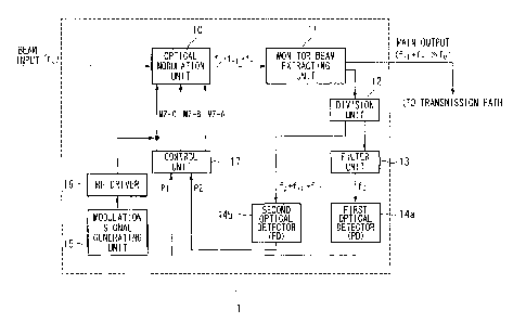
FIG 1 is a functional block diagram illustrating an optical modulation device
1
according to a first embodiment of the invention.
10 In the figure, a laser beam having a frequency fo is emitted from a
light source
(not shown) to an optical modulation unit 10. The optical modulation unit 10,
which
includes an optical waveguide having a predetermined structure and an
electrode, is an
optical waveguide element (of which details are described below with reference
to FIG
2) formed of an LN board. The optical modulation unit 10 modulates an input
beam
into a modulation signal having a frequency fm and outputs beams having
components of
frequencies fo, f-f, and f, where f+i---fo-f-fm and fi=fo¨fm. In addition,
when the input
beam is modulated into a beam having the frequency fm, a high order component
foH-2fin
or fo+3fm is generated. However, in the embodiments, the high order component
is
ignored for simple description.
The output beam passing through a monitor beam extracting unit 11 is output as
a main output beam from the optical modulation device 1 to be transmitted
through a
transmission medium (optical fiber). At this time, a part of the output beam
is extracted
as a monitor beam used to control the optical modulation unit 10 by the
monitor beam
extracting unit 11, and then is supplied to a division unit 12. The monitor
beam
extracting unit 11 is formed of a fiber type optical coupler. For example, a
division ratio
CA 02649623 2008-10-17
11
of the monitor beam is configured to -10 dll (main output beam: monitor beam =
10:1).
The beam supplied to the division unit 12 is divided into two beams by the
division unit 12. One of the divided beams is input to a first optical
detector 14a via the
filter unit 13 and the other of the divided beams is just input to a second
optical detector
14b.
The division unit 12 is a fiber type optical coupler which is the same as the
monitor optical extracting unit 11. In order for the first optical detector
14a to precisely
detect a small quantity of beam having a component of frequency fo, it is
preferable to set
the division ratio to -10 dB in the second optical detector 14b, for example,
as described
below.
The filter unit 13 extracts the component of frequency fo from the components
of
frequencies (fo, and f..1) of the input beam to output it to the first
optical detector 14a.
FIG 3 is a diagram illustrating a specific configuration example of the filter
unit
13. The filter unit 13 has a configuration in which two pairs of optical
circulators 131
and fiber bragg gratings (FBG) 132 are connected in series to each other.
The beam input to the filter unit 13 is sent to a front-side fiber bragg
grating 132
via a front-side optical circulator 131 (where the optical circulators 131 are
optical
elements which output a beam in a direction indicated by an arrow in a circle
in the
figure). The fiber bragg gratings 132 are optical elements in which a
diffraction grating
having a predetermined pitch is formed and reflect only a beam having a
wavelength
(frequency) corresponding to the pitch. In this case, it is assumed that the
fiber bragg
gratings 132 selectively reflecting the beam having the component of frequency
fo are
used (in both the front-side and rear-side). The beam having the frequency fo
reflected
by the front-side fiber bragg grating 132 is sent to the rear-side optical
circulator 131 via
the front-side optical circulator 131.
CA 02649623 2008-10-17
12
Likewise, in the rear-side fiber bragg grating, the beam having the component
of
frequency fo is selectively reflected in the same manner. In this way, the
beam having
only the frequency fo is output from the filter unit 13.
In the filter unit 13, two pairs of fiber bragg gratings having the same
filter
function are connected in series to each other. In this way, by configuring
multi-pairs of
fiber bragg gratings, it is possible to select a frequency of the filtered
beam more
precisely, thereby improving control precision, which will be described below.
In the filter unit 13 using the fiber bragg gratings 132, it is preferable to
perform
a reflection-free termination treatment on rear portions (lower portion in the
figure) of the
fiber bragg gratings 132 in order to prevent the beam having the components of
frequencies fq and El transmitting through the fiber bragg gratings 132 from
reflecting
from a forward path and being mixed with the output beam of the filter unit.
Generally, upon selecting the wavelength of the fiber bragg gratings 132, a
selection property depends on a temperature. Accordingly, it is preferable to
put the
filter unit 13 in a constant-temperature bath to maintain its temperature.
In FIG 1, the beam output from the filter unit 13 is input to the first
optical
detector 14a to measure a power P1 of the component of frequency fo. The
remainder
of the beam divided from the division unit 12 is input to the second optical
detector 14b
to measure a power P2 including the entire components of frequencies fo, f+1,
and f1.
Spectra of the beams input to the optical detectors are shown in FIGS. 4A and
4B. The
beam reception powers P1 and P2 correspond to powers of spectrum components
indicated by solid lines in the figure.
The first optical detector 14a and the second optical detector 14b are formed
of a
photo diode (PD) detecting a power (intensity) of the received beam. The beam
reception powers P1 and P2 are sent from the optical detectors to a control
unit 17.
CA 02649623 2008-10-17
13
The control unit 17 controls a modulation process of the optical modulation
unit
on the basis of the beam reception powers PI and P2. As described below, the
controlling are individually performed on three electrodes which are each
formed in
Mach-Zehnder optical waveguides (MZ-A, MZ-B, and MZ-C). In addition, the
control
5 unit 17 is realized by a personal computer or other general control
devices.
A modulation signal having the frequency fm in addition to a control signal
transmitted from the control unit 17 is input to the MZ-C. The modulation
signal which
is generated by a modulation signal generating unit 15 is a signal which is
converted into
voltage having a predetermined amplitude by an RF driver 16.
10 Next, the optical modulation unit 10 will be described with reference to
FIG. 2.
FIG. 2 is a diagram illustrating a configuration of the optical modulation
unit 10.
In the figure, the optical modulation unit 10 includes an optical waveguide
constituted by a main Mach-Zehrider optical waveguide (MZ-C) 101 and a first
sub-
Mach-Zehnder optical waveguide (MZ-A) 102 and a second sub-Mach-Zehnder
optical
waveguide (MZ-B) 103 each formed in arms of the MZ-C 101. In addition, the MZ-
A
102 and the MZ-B 103 are provided with DC electrode (first phase difference
adjusting
member) 106a and 106b which adjust a phase difference of a beam passing
through
respective arms of the Mach-Zehnder optical waveguides, respectively. The MZ-C
101
is provided with a DC electrode (second phase difference adjusting member) 104
which
makes a phase difference of a bias on the beam passing through the arms of the
Mach-
Zehnder optical waveguide and a modulation electrode (modulation member) 105
which
modulates a frequency of the beam into the frequency fr..
Although not shown, the optical modulation unit 10 is a unit in which
constituent
elements are formed on the LN board made of crystal having an electro-optic
effect. A
phase of the beam passing though the optical waveguide varies with variation
in a
CA 02649623 2008-10-17
14
refractive index of the optical waveguide by an electric field applied from
the respective
electrodes.
By varying input voltage in the DC electrodes 106a and 106b of the MZ-A 102
and the MZ-B 103, respectively, it is possible to adjust the phase difference
of the beam
passing through the arms of the sub-Mach-Zehnder optical wavelengths.
Accordingly,
it is possible to vary the intensity of the beam output from sub-Mach-Zehnder
optical
wavelengths.
By varying input voltage in the DC electrode 104 of the MZ-C 101, it is
possible
to adjust the phase difference of the beams (beams output from the MZ-A 102
and the
IvIZ-B 103) passing through the arms of the main Mach-Zehnder optical
waveguide.
Accordingly, it is possible to vary a modulation operating point of a
modulation process
(which is performed by the modulation electrode 105) in the main Mach-Zehnder
optical
waveguide.
For example, when the DC electrode 104 applies a phase difference of it, the
output of the optical modulation unit 10 at none-modulation time becomes zero
by
interfering in the output beams of the sub-Mach-Zchnder optical wavelengths to
be out-
phase.
When the modulation electrode 105 modulates a frequency of the output beams
into the frequency f,T, in this state, the sidebands occur in the frequencies
ffi and El and
the output beams are output as a modulation signal beam. However, when the
intensities of the output beams of the sub-Mach-Zehnder optical wavelengths
are
asymmetric, the output of the optical modulation unit 10 at none-modulation
time does
not become zero. Moreover, even at modulation time, the output beams are
output in a
state where the frequency fp remains (state in FIG. 4A).
In the optical modulation device 1, the phase difference applied by the
respective
CA 02649623 2008-10-17
DC electrodes 106a, 106b, and 104 of the MZ-A 102, the MZ-B 103, and the MZ-C
101,
respectively, is controlled using the beam reception powers P1 and P2 of the
beams
measured by the first optical detector 14a and the second optical detector
14b. In the
controlling, the DC electrodes 106a, 106b, and 104 are made adjusted so that
the beam
5 reception power P1 of the first optical detector 14a becomes a minimum
value and the
beam reception power P2 of the second optical detector 14b becomes a maximum
value.
A detail control sequence is as follows.
First, the beam reception powers P1 and P2 are set to become maximum values
by adjusting the three DC electrodes 106a, 106b, and 104 (first step). At this
time, in
10 the MZ-A 102 and the MZ-B 103, the phase difference in the respective
arms becomes
zero and the intensities of the output beams of the sub-Mach-Zehrider optical
wavelengths become the maximum value (in this case, asymmetric). In addition,
in the
MZ-C 101, the phase difference (the phase difference between the output beams
of the
sub-Mach-Zehnder optical wavelengths) in the two arms is zero.
15 Next, the beam reception power PI is set to the minimum value by
adjusting the
DC electrode 104 of the MZ-C 101 (second step). At this time, in the MZ-C 101,
the
phase difference of the output beams of the sub-Mach-Zehnder optical
wavelengths
becomes 'a and the intensity of the component of frequency fo in the output
beam of the
optical modulation unit 10 becomes a minimum value. However, since the
intensities of
the output beams of the sub-Mach-Zehnder optical wavelengths remain to be
asymmetric,
the component of frequency fo remains and does not become zero (minimum value
of
truth).
Subsequently, the DC electrode (the DC electrode 106a in this case) of which
the
beam reception power P1 varies so as to be reduced by gradually adjusting the
DC
electrode 106a of the MZ-A 102 and the DC electrode 106b of the MZ-B 103 is
selected.
CA 02649623 2008-10-17
16
Subsequently, the beam reception power P1 is set to the minimum value of truth
by
adjusting the elected DC electrode 106a again (third step). At this time, the
large
intensity of the output beam of the MZ-A 102 is attenuated by the adjusting of
the phase
difference by the DC electrode 106a to be adjusted to the intensity of the
output beam of
the MZ-B 103. As a result, the component of frequency fo becomes zero and the
beam
having the components of frequencies f+) and f_i is output from the optical
modulation
unit 10, thereby realizing a high extinction ratio of an ON state to an OFF
state in the
modulation of the modulation signal fm.
After the controlling is performed in the first to third steps, a phase of the
output
beam of the respective Mach-Zehnder optical waveguides may varies with time
elapsed
because of variation in ambient temperature, for example. In order to correct
the
variation in the ambient temperature, the optical modulation can be realized
with higher
precision by repeatedly performing the controlling in the second and third
steps
constantly or at regular intervals.
In this embodiment, the beam having components of frequencies fo, fi-1, and Li
which is output from the optical modulation unit 10 is monitored; the beam
reception
power P2 of the entire frequencies is measured by the second optical detector
14b while
the beam reception power P1 of the component of frequency fo filtered by the
filter unit
13 is measured by the first optical detector 14a; and the phase difference
applied by the
DC electrodes of the Mach-Zehnder optical wavelengths MZ-A, MZ-B, and MZ-C of
the
optical modulation unit 10 is controlled on the basis of the beam reception
powers P1 and
P2. The controlling is performed by setting the beam reception power P1 to
the
minimum value and the beam reception power P2 to the maximum value. In this
way,
the controlling of the phase difference can be performed while performing the
modulation process to optimize the extinction ratio. Accordingly, a high
extinction ratio
CA 02649623 2008-10-17
17
can be reliably obtained in real time even while the optical modulation device
I
practically operates in an optical communication system.
(Second Embodiment)
In the fist embodiment, the controlling is performed using the beam reception
power PI of the component of frequency fo and the beam reception power P2 of
the
entire components of frequencies. However, instead of the beam reception power
P2 of
the entire components of frequencies, the controlling may be performed using a
beam
reception power P3 of the components of frequencies f,-1 and L1.
According to a second embodiment, an optical modulation device 2 has a
structure shown in FIG 5.
In FIG. 5, a monitor beam extracted by the monitor beam extracting unit 11 is
input to a division unit 18 to be divided into two beams: a beam having the
component of
frequency fo and a beam having the components of frequencies and F1. A beam
reception power P1' of the former beam is measured by a third optical detector
14c and a
beam reception power P3 of the latter beam is measured by a fourth optical
detector 14d.
In this embodiment, spectra of the beams input by the optical detectors are
shown in
FIGS. 6A and 68.
The control unit 17 of the optical modulation device 2 controls a modulation
process of the optical modulation unit 10 on the basis of the beam reception
powers P1'
and P3. In the controlling, the DC electrodes 106a. I06b, and 104 are adjusted
so that
the beam reception power P1' of the third optical detector 14c becomes a
minimum value
and the beam reception power P3 of the fourth optical detector 14d becomes a
maximum
value. A difference from the first embodiment is that the beam reception
powers P1'
and P3 are used instead of the beam reception powers P1 and P2. In addition, a
detailed
control sequence is the same as the above-described sequence.
CA 02649623 2008-10-17
18
The division unit 18 functions as dividing the input beam (which has the
components of frequencies fo, fqn, and f..1) into the beam having the
component of
frequency fo and the beam having the components of frequencies and fn
Specifically, for example, the optical circulator 131 and the fiber bragg
grating 132
described above are combined to realize a desired function (in this case, one
pair is
configured unlike the filter unit 13). By using a generally used optical
element capable
of selecting a wavelength, the beam having the component of frequency fo is
reflected (or
transmitted) and the beam having the components of frequencies f+1 and Li is
transmitted
(or reflected), so that the optical circulator extracts the reflected beam.
The embodiments of the invention have been described with reference to the
drawings. However, the detailed configuration is not limited to the above-
described
configurations, but may be modified in various forms without departing the
gist of the
invention.
For example, the single modulation frequency fm generated by the above-
described modulation signal generating unit 15 is used to perform the
modulation process
by the optical modulation unit 10. However, even when a data signal to be
transmitted
is generated by the modulation signal generating unit 15 the data signal is
used to
perform the modulation process, a high extinction ratio can be realized in the
same
control manner.
The detail configuration is not limited as long as the filter unit 13 includes
an
element having an optical filter function based on a known technique. For
example, a
dielectric multiplayer filter or the like which uses interference by multiple
films may be
applied.
When automatic control is not necessary, the control unit 17 may manually
operate.
CA 02649623 2008-10-17
19
As a light source of the laser beam input to the optical modulation unit 10,
for
example, there is used a DFB laser which is stably controlled with wavelength
precision
< 1 Gliz and beam output power precision < 0.1 dB. Accordingly, a satisfactory
result can be obtained.
INDUSTRIAL APPLICABILITY
According to the invention, it is possible to provide an optical modulation
device
which can stably realize a high extinction ratio while performing a modulation
process by
modulation signals.