Note: Descriptions are shown in the official language in which they were submitted.
CA 02650164 2009-01-19
TITLE: BIPOLAR (DIS)CHARGING LED DRIVE METHOD AND
CIRCUIT THEREOF
BACKGROUND OF THE INVENTION
(a) Field of the Invention
The present invention is related to an innovative circuit design of
LED drive method and circuit that can be driven by AC or by a DC power
source with period of polarity exchange, and more particularly, to one
that the operation function is through the capacitor to produce bipolar
charging/discharging electric power to drive the light emitting diode, so
as to have the advantages of low thermal loss, power consumption, and
production cost.
(b) Description of the Prior Art:
i s Whereas conventionally a drive circuit in a light emitting diode
driven by AC, or by a DC power source with period of polarity exchange
has to be always comprised of a bridge rectification and a drop limiting
resistance, thermal loss, wasted power, and increased production cost
resulted from the light emitting diode has its flaws both of bridge
rectification and drop limiting resistance are the flaws found with the
LED of the prior art.
SUMMARY OF THE INVENTION
The primary purpose of the present invention is to provide a bipolar
(dis)charging LED drive method and circuit thereof. The present
invention is comprised of a first component and a second component in
series connection of reversed polarity. The first component includes a
diode series connected of forward polarity with an illuminating conduct
polarity of a light emitting diode before being parallel connected with a
bipolar capacitor; and the second component is either constituted by a
-1-
CA 02650164 2009-01-19
diode and a bipolar capacitor in series connection, or the diode can be
selected as needed to series connect with an optional light emitting diode,
thereby the constitution method of the second component includes:
(1) when the optional light emitting diode is selected to be installed,
the diode may be series connected with the light emitting diode at
forward polarity with the illuminating conduct polarity of the light
emitting diode before being parallel connected with a bipolar capacitor,
thereby to constitute a first type of the second component; and
(2) if the optional light emitting diode is selected not to be installed
in the second component, the diode is parallel connected with the bipolar
capacitor to constitute a second type of the second component.
The first component is connected in series of reversed polarity with
either type of the second component to constitute a LED drive circuit
(U100) capable of charging and discharging. The two ends of the LED
i5 drive circuit (U100) capable of charging and discharging are for
inputting:
(1) The AC power with constant or variable voltage and constant or
variable frequency; or
(2) The electric power with constant or variable voltage and constant
or variable polarities alternated periods converted from DC power source;
or
(3) The electric power with constant or variable voltage and constant
or variable polarities alternated periods converted from DC power which
is further rectified from AC power.
BRIEF DESCRIPTION OF THE DRAWINGS
Fig. 1 is a schematic view showing a basic circuit configuration of
the present invention.
Fig. 2 is a circuit example schematic diagram showing a zener diode
is further installed to a light emitting diode in the circuit of Fig. 1.
-2-
CA 02650164 2009-01-19
Fig. 3 is a circuit example schematic diagram showing that a
charge/discharge device can be parallel connected across the two ends of
a current limiting resistance and a light emitting diode in series
connection in the circuit of Fig. 2.
Fig. 4 is a circuit example schematic block diagram showing that the
present invention is series connected to an AC power modulator of series
connection type.
Fig. 5 is a circuit example schematic block diagram showing that the
present invention is parallel connected with an AC power modulator of
parallel connection type.
Fig. 6 is a circuit example schematic block diagram showing that the
present invention is series connected to a modulated periodically
polarities alternated power modulator of series connection type.
Fig. 7 is a circuit example schematic block diagram showing that the
present invention is parallel connected with a modulated periodically
polarities alternated power modulator of parallel connection type.
Fig. 8 is a circuit example schematic block diagram showing that the
present invention is series connected to a modulated periodically
polarities alternated power modulator of series connection type before is
electrically driven by an output from DC to AC inverter.
Fig. 9 is a circuit example schematic block diagram showing that the
present invention is parallel connected with a modulated periodically
polarities alternated power modulator of parallel connection type before
is electrically driven by an output from a DC to AC inverter.
Fig. 10 is a circuit example schematic block diagram showing that
the present invention is electrically driven by an output from a DC to AC
inverter.
Fig. 11 is a circuit example schematic block diagram showing that
the present invention is series connected with an impedance component.
Fig. 12 is a circuit example schematic block diagram showing that
-3-
CA 02650164 2009-01-19
the impedance components connected in series to the present invention
executes series connection, parallel connection, or series and parallel
connection by means of the switching device.
DESCRIPTION OF MAIN COMPONENT SYMBOLS
C201, C202: Bipolar capacitor
CR101, CR102, CR201, CR202: Diode
ESD101, ESD 102: Charge/discharge device
1103, 1104: Inductive impedance component
LED101, LED102: Light emitting diode
R101, R102: Discharge resistor
R103, R104: Current limit resistor
U100: LED drive circuit capable of charging and discharging
U 101: The first component
i s U102: The second component
ZD 101, ZD 102: Zener diode
300: AC power modulator of series connection type
310: AC power modulator of parallel connection type
400: Modulated periodically polarities alternated power modulator of
series connection type
410: Modulated periodically polarities alternated power modulator of
parallel connection type
500: Impedance component
600: Switching device
4000: DC to AC Inverter
DETAILED DESCRIPTION OF THE PREFERRED EMBODIMENTS
A bipolar (dis)charging LED drive method and circuit thereof
disclosed in the present invention is comprised of a first component and a
second component in series connection of reversed polarity. The first
-4-
CA 02650164 2009-01-19
component is constituted by a diode connected in series of forward
polarity with an illuminating conduct polarity of a light emitting diode
before being connected in parallel with a bipolar capacitor; and the
second component is either constituted by a diode and a bipolar capacitor
in series connection, or the diode can be selected as needed to series
connect with an optional light emitting diode. The constitution methods
of the second component include: (1) when the optional light emitting
diode is selected to be installed, the diode may be series connected with
the light emitting diode at forward polarity with the illuminating conduct
polarity of the light emitting diode before being parallel connected with a
bipolar capacitor, thereby to constitute a first type of the second
component; and (2) if the optional LED is selected not to be installed in
the second component, the diode is parallel connected with the bipolar
capacitor to constitute a second type of the second component.
The first component is connected in series of reversed polarity with
either type of the second component to constitute an LED drive circuit
(U100) capable of charging and discharging. The two ends of the LED
drive circuit (U100) capable of charging and discharging are for
inputting:
(1) The AC power with constant or variable voltage and constant or
variable frequency; or
(2) The electric power with constant or variable voltage and constant
or variable polarities alternated periods converted from DC power source;
or
(3) The electric power with constant or variable voltage and constant
or variable polarities alternated periods converted from DC power which
is further rectified from AC power.
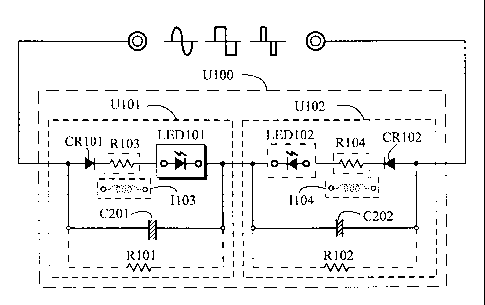
Referring to Fig. 1 is a schematic view of a basic circuit
configuration of the present invention.
As illustrated in Fig.l, the bipolar (dis)charging LED drive method
-5-
CA 02650164 2009-01-19
and circuit thereof is using the bipolar capacitors (C201), (C202) to
constitute the first component (U 101) and the second component (U 102)
respectively, wherein it is essentially comprised including:
A bipolar capacitor: it is comprised of bipolar capacitors (C201),
(C202) that are capable of bipolar charging and discharging, wherein said
bipolar capacitors may be of same or different electric capacity;
The first component (UlOl): it is comprised of a diode (CR101)
capable of executing uni-directional conduction in series connection of
forward polarity to at least one light emitting diode (LED101) before
being parallel connected with a bipolar capacitor, thereby to constitute the
first component (U 101);
The second component (U102): it is comprised of a diode (CR102)
capable of executing uni-directional conduction in series connection of
forward polarity to at least one light emitting diode (LED 102) before
being parallel connected with a bipolar capacitor, thereby to constitute the
second component (U 102);
In addition, if the light emitting diode (LED 102) is selected not to be
installed as needed, the diode (CR102) can be directly parallel connected
with the bipolar capacitor (C202), thereby to constitute the second
component (U 102);
The first component (U101) and the second component (U102) are
series connected of reversed polarity to constitute the LED drive circuit
(U 100) capable of charging and discharging, whereof the two ends of the
LED drive circuit (U100) capable of charging and discharging is arranged
for inputting:
(1) The AC power with constant or variable voltage and constant or
variable frequency; or
(2) The electric power with constant or variable voltage and constant
or variable polarities alternated periods converted from DC power source;
or
-6-
CA 02650164 2009-01-19
(3) The electric power with constant or variable voltage and constant
or variable polarities alternated periods converted from DC power which
is further rectified from AC power.
In the LED drive circuit (U100) capable of charging and discharging,
multiple matching modes are available for choice among the light
emitting diode (LED 101) constituting the first component (U 101), and
the light emitting diode (LED 102) constituting the second component
(U102) as follows:
1. The light emitting diode (LED 101) is comprised of one or a
plurality of light emitting diodes;
2. If the second component (U102) is selected to include the light
emitting diode (LED102), the light emitting diode (LED102) is
comprised of one or a plurality of light emitting diodes;
3. The constitution ways of the light emitting diode (LED 101) or
ss light emitting diode (LED102) include to be constituted individually by
one light emitting diode of forward illuminating current polarity, or to be
constituted by two or more than two light emitting diodes of forward
illuminating current polarity in series or parallel connection, or to be
constituted by three or more than three light emitting diodes of forward
illuminating current polarity in series connection, parallel connection or
series-parallel connection;
4. The numbers of light emitting diodes which constitute the light
emitting diode (LED101) and the numbers of light emitting diodes which
constitute the light emitting diode (LED102) can be the same or different;
5. Whereas the electric power source is related to an AC power
source, or a bi-directional power source with polarity alternated periods
that is converted from a DC power source, the light emitting diode
(LED101) or the light emitting diode (LED102) is not continuously
conducted by the DC power, thus to allow selection of a peak value of the
working voltage for each light emitting diode referring to the inputted
-7-
CA 02650164 2009-01-19
voltage wave shape and duty, cycle of current conduction and
disconnection, as well as a selected working current value. The
selections include (1) having a voltage lower than a normal rated voltage
as the peak voltage; (2) having the normal rated voltage as the peak
voltage; and (3) having a voltage higher than the normal rated voltage as
the peak voltage;
The present invention works on having a supply of power source
with a polarity to charge the bipolar capacitor (C202) from the second
component (U 102) through the diode (CR101) and the light emitting
diode (LED 101) from the first component (U 101), and the charged
electric power keeps the light emitting diode (LED101) illuminated; and
having the supply of power source with the other polarity to charge the
bipolar capacitor (C201) from the first component (U101) through the
diode (CR102) and the light emitting diode (LED102) from the second
component (U102), and the charged electric power keeps the light
emitting diode (LED102) illuminated. If the second component (U102) is
not disposed with the light emitting diode (LED102), the electric power
directly charges the bipolar capacitor (C201) from the first component
(U101) through the diode (CR102) of the second component (U102).
When applied in practical applications, the LED drive circuit (U100)
capable of charging and discharging as illustrated in Fig. 1 may be
optionally disposed with multiple auxiliary circuit components as
applicable_including the selection of either to be or not to be installed as
needed and the selection of the installed quantity to be one or more than
ones. In case of more than one components are selected, they can be in
series connection, parallel connection or series-parallel connection of
selected polarity relationship according to the requirements of the circuit
function; the constituted components and the optional auxiliary circuit
devices including:
The discharging resistance (R101): it is an optional device
-8-
CA 02650164 2009-01-19
connected in parallel with both ends of the bipolar capacitor (C201) from
the first component (U101) to discharge residual electric charge from the
bipolar capacitor (C201);
The discharging resistance (R102): it is an optional device
connected in parallel with both ends of the bipolar capacitor (C202) from
the second component (U102) to discharge residual electric charge from
the bipolar capacitor (C202);
The current limiting resistance (R103): it is an optional device which
is arranged to be respectively connected in series to the diode (CR101)
and the light emitting diode (LED 101) from the first component (U 101)
to limit currents passing through the light emitting diode (LED101); the
current limiting resistance (R103) may be replaced with an inductive
resistance (1103);
The current limiting resistance (R104): it is an optional device which
is arranged to be respectively connected in series to the diode (CR102)
and the light emitting diode (LED102) from the second component (U102)
to limit currents passing through the light emitting diode (LED102); the
current limiting resistance (R104) may be replaced with an inductive
resistance (1104);
In addition, to avoid the light emitting diode being damaged or
reduced service life by abnormal voltage, in the LED drive circuit (U100)
capable of charging and discharging of the present invention, a zener
diode may be further connected in parallel with both ends of the light
emitting diode; or at least one zener diode may be series connected with
at least one diode to jointly generate zener voltage function for parallel
connecting to both ends of the light emitting diode, as illustrated in Fig. 2
showing a circuit example schematic diagram of having added the zener
diode to the light emitting diode in the circuit illustrated in Fig. 1.
Detailed description is as follows:
In the circuit examples as illustrated in Fig. 2, a zener diode (ZD 101)
-9-
CA 02650164 2009-01-19
is parallel connected to both ends, of the light emitting diode (LED101)
from the first component (U 101) to protect the light emitting diode,
whereof their polarity relationship is that the zener voltage of the zener
diode (ZD 101) is used to limit the working voltage across the two ends of
the light emitting diode (LED 101); as applicable, the diode (CR201) may
be selected to be series connected with the zener diode (ZD 101), whereof
providing advantages of (1) protecting the zener diode (ZD 101) against
reversed current; and (2) achieving temperature compensation results
between the zener diode (ZD 101) and the diode (CR201).
When the light emitting diode (LED102) is selected to be included
in the second component (U102), a zener diode (ZD102) is parallel
connected with both ends of the light emitting diode (LED102), whereof
their polarity relationship is that the zener voltage of the zener diode
(ZD102) is used to limit the working voltage across the two ends of the
light emitting diode (LED102); as applicable, the diode (CR202) may be
selected to be series connected with the zener diode (ZD 102), whereof
providing advantages of (1) protecting the zener diode (ZD 102) against
reversed current; and (2) achieving temperature compensation results
between the zener diode (ZD102) and the diode (CR202).
To achieve the lighting stability of the light source produced by the
light emitting diode and reduce the lighting pulsation, in the LED drive
circuit (U100) capable of charging and discharging, both or at least one of
the first component (U 10l ) and the second component (U 102) can be
further installed with a charge/discharge device. Fig. 3 shows a circuit
example schematic diagram that a charge/discharge device is parallel
connected across the two ends of the light emitting diode and the series
connected current limiting resistance in the circuit of Fig. 2.
In the circuit examples as illustrated in Fig. 3, to promote the
lighting stability of the light source produced by the light emitting diode,
the two ends of the light emitting diode (LED 101) and the current
-10-
CA 02650164 2009-01-19
limiting resistance (R103) in series connection from the first component
(U l O 1), or directly at the two ends of the light emitting diode (LED 1 O 1)
can be further parallel connected with a charge/discharge device
(ESD 101) according to the polarity for randomly charging or discharging
the electric power, whereby to stabilize the operation of light emission
from the light emitting diode (LED101). If the light emitting diode
(LED102) is selected for the second component (U102), a
charge/discharge device (ESD 102) can be selected as needed to be
parallel connected with the two ends of the light emitting diode (LED 102)
and the current limiting resistance (R104) in series connection, or directly
parallel connected at the two ends of the light emitting diode (LED 102)
according to the polarity for randomly charging or discharging the
electric power, whereby to stabilize the operation of light emission from
the light emitting diode (LED 102).
1s The charge/discharge devices (ESD101) and (ESD102) can be
constituted by the conventional charging and discharging batteries, or
super-capacitors or capacitors, etc.
In addition, the bipolar (dis)charging LED drive method and circuit
thereof of the present invention, whereof both or at least one of the first
component (U 101) and the second component (U 102) can be further
disposed with the charge/discharge devices (ESD101), (ESD102) for
randomly charging or discharging the electric power, whereby to stabilize
the operation of light emission from the light emitting diodes (LED 101)
and (LED 102); and in case of power failure, either or both of the reserved
electric power in the charge/discharge devices (ESD101) and ESD 102
discharges the reserved electric power, so as to continue supplying power
to maintain at least one of the light emitting diode (LED 101) or (LED 102)
illuminated.
The first component (U101), the second component (U102), the light
emitting diodes (LED 1 O 1), (LED 102) as well as various aforesaid
-11-
CA 02650164 2009-01-19
optional auxiliary circuit components as illustrated in Figs. 1 through 3
are based on application needs to be optionally installed or not installed
as needed, and the installation quantity include constitution by one or
more than ones, wherein if more than one components are selected in the
application, they can be in series connection, parallel connection, or
series-parallel connection of selected polarity relationship according to
the requirements of the circuit function; whereby the constituted
components and optional auxiliary circuit components including:
1. The first component (U 101) can be constituted by one or by
more than ones in series connection, parallel connection, or series-parallel
connection;
2. The second component (U102) can be constituted by one or by
more than ones in series connection, parallel connection, or series-parallel
connection;
3. The light emitting diode (LED101) can be constituted by one
light emitting diode of forward illuminating current polarity, or by two or
more than two light emitting diodes in series or parallel connection of
forward illuminating current polarity, or by three or more than three light
emitting diodes in series connection, parallel connection, or
series-parallel connection of forward illuminating current polarity;
4. The light emitting diode (LED102) can be constituted by one
light emitting diode of forward illuminating current polarity, or by two or
more than two light emitting diodes in series or parallel connection of
forward illuminating current polarity, or by three or more than three light
emitting diodes in series connection, parallel connection, or
series-parallel connection of forward illuminating current polarity;
5. The discharging resistance (R101) can be constituted by one or
by more than ones in series connection, parallel connection, or series-
parallel connection;
6. The discharging resistance (R102) can be constituted by one or
-12-
CA 02650164 2009-01-19
by more than ones in series connection, parallel connection, or
series-parallel connection;
7. The current limiting resistance (R103) can be constituted by one
or by more than ones in series connection, parallel connection, or
series-parallel connection;
8. The current limiting resistance (R104) can be constituted by one
or by more than ones in series connection, parallel connection, or
series-parallel connection;
9. The current limiting inductive resistance (1103) can be
constituted by one or by more than ones in series connection, parallel
connection, or series-parallel connection;
10. The current limiting inductive resistance (1104) can be
constituted by one or by more than ones in series connection, parallel
connection, or series-parallel connection;
11. The diode (CR101) can be constituted by one diode, or by more
than one diodes in series connection of forward polarity, or in parallel
connection of the same polarity, or in series-parallel connection;
12. The diode (CR102) can be constituted by one diode, or by more
than one diodes in series connection of forward polarity, or in parallel
connection of the same polarity, or in series-parallel connection;
13. The zener diode (ZD 10 1) can be constituted by one zener diode,
or by more than one zener diodes in series connection of forward polarity,
or in parallel connection of the same polarity, or in series-parallel
connection;
14. The zener diode (ZD 102) can be constituted by one zener diode,
or by more than one zener diodes in series connection of forward polarity,
or in parallel connection of the same polarity, or in series-parallel
connection;
15. The diode (CR201) can be constituted by one diode, or by more
than one diodes in series connection of forward polarity, or in parallel
-13-
CA 02650164 2009-01-19
connection of the same polarity, or, in series-parallel connection;
16. The diode (CR202) can be constituted by one diode, or by more
than one diodes in series connection of forward polarity, or in parallel
connection of the same polarity, or in series-parallel connection;
17. The charge/discharge device (ESD101) can be constituted by
one charge/discharge device or by more than one charge/discharge
devices in series connection of forward polarity, or in parallel connection
of the same polarity, or in series-parallel connection;
18. The charge/discharge device (ESD102) can be constituted by
one charge/discharge device or by more than one charge/discharge
devices in series connection of forward polarity, or in parallel connection
of the same polarity, or in series-parallel connection;
When applied, the bipolar (dis)charging LED drive method and
circuit thereof of the present invention can provide for inputting:
(1) The AC power with constant or variable voltage and constant or
variable frequency; or
(2) The electric power with constant or variable voltage and constant
or variable polarities alternated periods converted from DC power source;
or
(3) The electric power with constant or variable voltage and constant
or variable polarities alternated periods converted from DC power which
is further rectified from AC power.
In addition, the present invention can be further incorporated with
the following active modulating circuit devices, whereof the active
modulating circuit devices include:
-- The AC power modulator of series connection type (300): It is
constituted by the conventional electromechanical components or solid
state power components and related electronic circuit components to be
series connected to the LED drive circuit (U100) capable of charging and
discharging for receiving the electric power from AC power source, so as
-14-
CA 02650164 2009-01-19
to execute power modulations including pulse width modulation (PWM),
conduction phase angle control, and impedance modulation to the AC
power with constant or variable voltage and constant or variable
frequency from the power source;
-- The AC power modulator of parallel connection type (310): It is
constituted by the conventional electromechanical components or solid
state power components and related electronic circuit components,
whereof its output ends are arranged to be parallel connected to the LED
drive circuit (U 100) capable of charging and discharging while its input
ends are arranged to receive the AC power, so as to execute power
modulations including pulse width modulation (PWM), conduction phase
angle control, and impedance modulation to the AC power with constant
or variable voltage and constant or variable frequency from the power
source;
-- The modulated periodically polarities alternated power modulator
of series connection type (400): It is constituted by the conventional
electromechanical components or solid state power components and
related electronic circuit components for series connected to the LED
drive circuit (U 100) capable of charging and discharging for receiving
electric power from the power source, so as to execute power modulations
including pulse width modulation (PWM), conduction phase angle
control, and impedance modulation to either the electric power with
constant or variable voltage and constant or variable polarities alternated
periods converted from DC power, or the electric power with constant or
variable voltage and constant or variable polarities alternated periods
converted from DC power which is further rectified from the AC power
source;
-- The modulated periodically polarities alternated power modulator
of parallel connection type (410): It is constituted by the conventional
electromechanical components or solid state power components and
-15-
CA 02650164 2009-01-19
related electronic circuit components, whereof its output ends are
arranged to be parallel connected to the LED drive circuit (U 100) capable
of charging and discharging while its input ends are arranged to receive
the electric power from power source, so as to execute power modulations
including pulse width modulation (PWM), conduction phase angle
control, and impedance modulation to either the electric power with
constant or variable voltage and constant or variable polarities alternated
periods converted from DC power, or the electric power with constant or
variable voltage and constant or variable polarities alternated periods
converted from DC power which is further rectified from the AC power
source;
-- The DC to AC inverter (4000): It is constituted by the
conventional electromechanical components or solid state power
components and related electronic circuit components, whereof its input
1s ends are arranged to receive DC power with constant or variable voltage
as selected while its output ends are arranged to output electric power of
bi-directional sinusoidal wave, or bi-directional square wave or
bi-directional pulsed wave with constant or variable voltage and constant
or variable polarity alternated periods;
-- The impedance (500): it is comprised of at least one resistive
impedance component, inductive impedance component and/or a
capacitive impedance component or comprised of at least two or at least
two kinds of impedance components mixed to execute series connection,
parallel connection or series-parallel connection, whereby to provide DC
impedance or AC impedance; or the capacitive impedance component and
the inductive impedance component are mutually series connected to
have the same frequency of the bi-directional electric power such as AC
power from the power source or the same polarities alternated periods of
the electric power with constant or variable voltage and constant or
variable polarities alternated periods converted from DC power, thereby
-16-
CA 02650164 2009-01-19
to appear a series resonance status,and a corresponding end voltage status
of series resonance across the two ends of the corresponding capacitive
impedance component or inductive impedance component; or the
capacitive impedance component and the inductive impedance
component are mutually parallel connected to have the same frequency of
the bi-directional electric power such as AC power from the power source
or the same polarities alternated periods of the electric power with
constant or variable voltage and constant or variable polarities alternated
periods, thereby to appear a parallel resonance status and corresponding
end voltage;
-- The switching device (600): it is constituted by
dynamo-mechanical switching devices or solid-state switching devices to
be arranged to modulate at least two impedance components (500) to
execute switches among series, parallel, and series-parallel connections;
The bipolar (dis)charging LED drive method and circuit thereof of
the present invention can constitute various application circuits as
following by incorporating one kind of above mentioned active power
modulators:
1. The present invention is series connected to an AC power
modulator; wherein the LED drive circuit (U 100) capable of charging and
discharging is series connected to the conventional AC power modulator
of series connection type (300) before driven by the inputted AC power
with constant or variable voltage and constant or variable frequency,
thereby to modulate the inputted power of the LED drive circuit (U100)
capable of charging and discharging, whereof the connection method is to
series connect the two devices; as illustrated in Fig. 4 is a circuit example
schematic block diagram showing the present invention is series
connected to an AC power modulator of series connection type;
2. The present invention is parallel connected with an AC power
modulator; wherein the LED drive circuit (U 100) capable of charging and
-17-
CA 02650164 2009-01-19
discharging is parallel connected with the output ends of the conventional
AC power modulator of parallel connection type (310) while the AC
power with constant or variable voltage and constant or variable
frequency is arranged to be inputted to the input ends of the AC power
modulator of parallel connection type (310), then delivered through the
output ends of the AC power modulator of parallel connection type (310)
to the LED drive circuit (U100) capable of charging and discharging for
modulating the inputted power of the LED drive circuit (U100) capable of
charging and discharging as illustrated in Fig. 5 for a circuit example
schematic block diagram of the present invention to be parallel connected
with an AC power modulator of parallel connection type;
3. The LED drive circuit (U100) capable of charging and
discharging is series connected to the conventional modulated
periodically polarities alternated power modulator of series connection
type (400) before receiving the electric power with constant or variable
voltage and constant or variable polarities alternated periods converted
from DC power, or the electric power with constant or variable voltage
and constant or variable polarities alternated periods converted from DC
power which is further rectified from the AC power, thereby to modulate
the inputted power of the LED drive circuit (U100) capable of charging
and discharging as illustrated in Fig. 6 for a circuit example schematic
block diagram showing that the present invention is series connected to a
modulated periodically polarities alternated power modulator of series
connection type;
4. The LED drive circuit (U100) capable of charging and
discharging is parallel connected with an output end of the conventional
modulated periodically polarities alternated power modulator of parallel
connection type (410); the electric power with constant or variable
voltage and constant or variable polarities alternated periods converted
from DC power, or the electric power with constant or variable voltage
-18-
CA 02650164 2009-01-19
and constant or variable polarities, alternated periods converted from DC
power which is further rectified from AC power is arranged to be inputted
to an input end of the modulated periodically polarities alternated power
modulator of parallel connection type (410) and then outputted from an
output end of modulated periodically polarities alternated power
modulator of parallel connection type (410) to the LED drive circuit
(U100) capable of charging and discharging for modulating the inputted
power of the LED drive circuit (U100) capable of charging and
discharging as illustrated in Fig. 7 for a circuit example schematic block
diagram of the present invention to be parallel connected with a
modulated periodically polarities alternated power modulator of parallel
connection type;
5. The LED drive circuit (U100) capable of charging and
discharging is series connected to the conventional modulated
1s periodically polarities alternated power modulator of series connection
type (400) before being parallel connected with an output end of the DC
to AC inverter (4000); a DC power with constant or variable voltage
selected as applicable is inputted into an input end of the DC to AC
inverter (4000) while the output end of the DC to AC inverter (4000)
outputs the electric power of bi-directional sinusoidal wave, or
bi-directional square wave or bi-directional pulsed wave with constant or
variable voltage and constant or variable polarities alternated periods
selected as applicable to the LED drive circuit (U100) capable of
charging and discharging for modulating the inputted power of the LED
drive circuit (U100) capable of charging and discharging as illustrated in
Fig. 8 for a circuit example schematic block diagram showing that the
present invention is series connected to a modulated periodically
polarities alternated power modulator of series connection type before
being driven by the electric power outputted from a DC to AC inverter;
so 6. The LED drive circuit (U100) capable of charging and
-19-
CA 02650164 2009-01-19
discharging is parallel connected with the an output end of the
conventional modulated periodically polarities alternated power
modulator of parallel connection type (410); a DC power with constant or
variable voltage selected as applicable is inputted into an input end of the
DC to AC inverter (4000) while the output end of the DC to AC inverter
(4000) outputs electric power of bi-directional sinusoidal wave, or
bi-directional square wave or bi-directional pulsed wave with constant or
variable voltage and constant or variable polarity alternated periods
selected as applicable to an input end of the modulated periodically
polarities alternated power modulator of parallel connection type (410)
before being outputted to the LED drive circuit (U100) capable of
charging and discharging through an output end of the modulated
periodically polarities alternated power modulator of parallel connection
type (410) for modulating the inputted power of the LED drive circuit
(U100) capable of charging and discharging as illustrated in Fig. 9 for a
circuit example schematic block diagram showing that the present
invention is parallel connected with a modulated periodically polarities
alternated power modulator of parallel connection type before being
driven by the electric power outputted from a DC to AC inverter;
7. The LED drive circuit (U100) capable of charging and
discharging is parallel connected with an output end of the conventional
DC to AC inverter (4000); a DC power with constant or variable voltage
selected as applicable is inputted into an input end of the DC to AC
inverter (4000) while the output end of the DC to AC inverter (4000)
outputs electric power of bi-directional sinusoidal wave, or bi-directional
square wave or bi-directional pulsed wave with constant or variable
voltage and constant or variable polarity alternated periods selected as
applicable to the LED drive circuit (U100) capable of charging and
discharging for modulating the inputted power of the LED drive circuit
(U100) capable of charging and discharging as illustrated in Fig. 10 for a
-20-
CA 02650164 2009-01-19
circuit example schematic block diagram showing that the present
invention is driven by the electric power outputted from a DC to AC
inverter;
8. The LED drive circuit (U100) capable of charging and
discharging is series connected to at least one conventional impedance
component (500) before being parallel connected with a power source;
wherein the impedance component (500) is comprised of:
(1) An impedance component (500): it is constituted by a
component with capacitive impedance characteristics; or
(2) An impedance component (500): it is constituted by a
component with inductive impedance characteristics; or
(3) An impedance component (500): it is constituted by a
component with resistive impedance characteristics; or
(4) An impedance component (500): it is constituted by a
Zs single impedance component with the combined impedance
characteristics of at least two characteristics of the resistive impedance, or
inductive impedance, or capacitive impedance simultaneously, thereby to
provide DC or AC impedances; or
(5) An impedance component (500): it is constituted by a
single impedance component with the combined impedance
characteristics of capacitive impedance and inductive impedance,
whereof its inherent resonance frequency is the same as the frequency of
the bi-directional electric power such as the AC power from the power
source or the polarities alternated periods of the electric power with
constant or variable voltage and constant or variable polarities alternated
periods converted from DC power, thereby to produce a parallel
resonance status; or
(6) An impedance component (500): it is constituted by
capacitive impedance components, or inductive impedance components,
or resistive impedance components, including one or more than one kind
-21-
CA 02650164 2009-01-19
of and one and more than one impedance component, or two or more than
two kinds of one or more than one impedance components in series
connection, or parallel connection, or series-parallel connections, thereby
to provide a DC or AC impedance;
Or the capacitive impedance component and the inductive impedance
component are in mutual series connection, whereby its inherent series
resonance frequency is the same as the frequency of bi-directional electric
power such as the AC power from power source, or the periods of the
periodically alternated polarities DC power converted from DC power,
thereby to produce an impedance status of series resonance status and
appear the corresponding end voltage of series resonance at the two ends
of corresponding capacitive impedance component or inductive
impedance component;
Or the capacitive impedance component and the inductive impedance
component are in mutual parallel connection, whereby its inherent
parallel resonance frequency is the same as the frequency of
bi-directional electric power such as the AC power from power source, or
the periods of the periodically alternated polarities DC power converted
from DC power, thereby to produce an impedance status of parallel
resonance status and appear the corresponding end voltage;
Fig. 11 is a circuit example schematic block diagram showing that the
present invention is series connected to an impedance component.
9. At least two impedance components (500) as said in the item 8
execute switches between series connection, parallel connection and
series-parallel connection by means of the switching device (600) which
is constituted by electromechanical components or solid state components,
whereby to modulate the power transmitted to the LED drive circuit
(U100) capable of charging and discharging, wherein Fig. 12 is a circuit
example schematic block diagram showing that impedance components
connected in series to the present invention executes series connection,
-22-
CA 02650164 2009-01-19
parallel connection, or series-parallel connection by means of a switching
device.
Colors of the individual light emitting diodes (LED 101) and (LED 102)
of the first component (U 101) and the second component (U 102) in the
bipolar (dis)charging LED drive method and circuit thereof can be
optionally selected to be constituted by one or more than one colors.
The relationships of location arrangement between the individual
light emitting diodes (LED 101) and (LED 102) of the first component
(U101) and the second component (U102) in the bipolar (dis)charging
LED drive method and circuit thereof include the following: 1)
sequentially linear arrangement; 2) sequentially distributed in a plane; 3)
crisscross-linear arrangement; 4) crisscross distribution in a plane; 5)
arrangement based on particular geometric positions in a plane; 6)
arrangement based on 3D geometric position.
Zs The bipolar (dis)charging LED drive method and circuit thereof, in
which it is constituted by circuit components which include: 1) It is
constituted by individual circuit components which are inter-connected; 2)
At least two circuit components are combined to at least two partial
functioning units which are further inter-connected; 3) All components
are integrated together to one structure.
Accordingly, a bipolar (dis)charging LED drive method and circuit
thereof the present invention provides advanced features of power saving,
low thermal loss and low cost in driving an LED by capacitance bipolar
charging and discharging operation.
-23-